SLYT817 September 2021 ADS8860 , OPA2991
1 Introduction
Operational-amplifier (op amp) circuits often perform system functions where the op amp needs to respond to input and output transients. Some circuits are designed primarily to accept different input transients, such as a sensor signal-conditioning circuit, while others supply output transients, such as an analog-to-digital converter (ADC) input or a reference driver. An often-overlooked aspect in op amp circuit design is the difference in output settling response times for an output (load) step vs. an input step for the same circuit.
In most circuits, the output load connects directly to the output of the op amp; the response time is largely based on the op amp’s ability to supply the required load transient and then recover. This behavior depends on the circuit topology, however. In circuits where the op-amp output voltage (Vopa) does not directly connect to the load, the output settling response can differ substantially from the input response. A common example of such a circuit, used in situations where the amplifier must drive a capacitive load (Cload), is the isolation resistor with dual-feedback (Riso+DFB) circuit topology. The name of the circuit comes from the use of an isolation resistor (Riso) between the Vopa and Cload nets and the two feedback paths back to the inverting input (IN-) from the feedback capacitor (Cf) and the feedback resistor (Rf).
Figure 1-1 shows an example Riso+DFB circuit used to drive a capacitive load (Cload). The input is directly connected to a voltage source, and therefore the op amp must react to changes that occur on the input. A simple switch (SW1) and resistive load (Rload) represent a rudimentary case where the output of the amplifier circuit experiences a load transient to which it must respond.
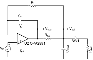 Figure 1-1 Riso with
dual-feedback schematic
Figure 1-1 Riso with
dual-feedback schematicThe two simulation circuits in Figure 1-2 demonstrate the differences in the output response between an input step and a load transient. Figure 1-2(a) applies an input voltage step to the input of the circuit, while Figure 1-2(b) applies a load current step to the output. In the load transient circuit, setting the voltage drop on the output formed from the load current (Iload) flowing through Riso (Iload x Riso) equal to the input step amplitude sets the initial change in Vopa to 10 mV in both circuits, enabling an equal comparison. A 10-mV output step amplitude prevents op-amp large-signal settling behavior, such as slew-rate limitations. In addition, the output current must be small enough to prevent the op amp from going into large-signal short-circuit current limits.
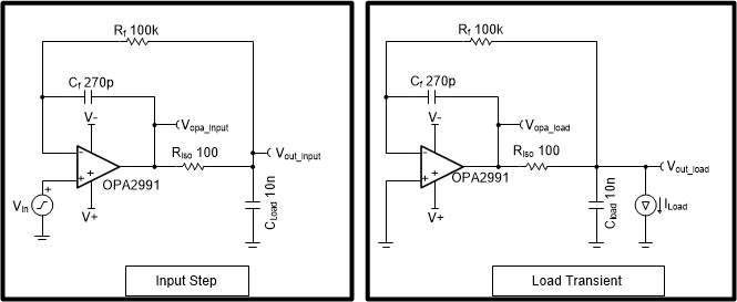 Figure 1-2 Input step (a) and load
transient (b) simulation circuits
Figure 1-2 Input step (a) and load
transient (b) simulation circuitsFigure 1-3 shows the results of the two simulation circuits. As designed, the initial change at Vopa is 10 mV for both input and output responses. But the time that it takes for the output voltage at the load (Vout) to settle is different between the two circuits; the input step circuit settles much faster than the output load transient step circuit. For example, to settle to 0.05%, equivalent to 10 bits, it takes 5.02 µs for the input step circuit and 189.42 µs for the output load transient circuit.
Table 1-1 lists the differences between the input step circuit and load transient step circuit output settling times required for 10- to 18-bit resolution acquisition systems for the circuit in Figure 1-2. Testing alternate op amps will result in different settling responses based on the finer effects created from their different output impedances and open-loop gain curves.
| Settling Accuracy Level | Input Step Transient Settling Time (µs) | Load Transient Settling Time (µs) |
|---|---|---|
| 10 bit (0.05%) | 5.02 | 189.42 |
| 12 bit (0.01%) | 39.94 | 230.23 |
| 14 bit (0.003%) | 71.01 | 261.06 |
| 16 bit (0.00076%) | 106.45 | 289.23 |
| 18 bit (0.00019%) | 142.23 | 347.08 |
 Figure 1-3 Output settling responses for
input step (a) and output load transient (b) circuits
Figure 1-3 Output settling responses for
input step (a) and output load transient (b) circuitsFigure 1-4 displays the components that dominate the output settling response for an input and output transient, as indicated by the red arrow. For an input step transient, the Riso and Cload resistor-capacitor (RC) time constant dominates the output settling time. When the input step occurs, Vopa immediately responds to the input voltage step. As the op-amp output voltage rises, Vout sees a delay because of Riso and Cload.
For a load transient, the Rf and Cf RC time constant dominates the output settling response. When a load transient occurs, Vout immediately drops by 10 mV (Riso x Iload). The time it takes for Vopa to respond to the drop in Vout is based on the RC time delay created by Rf and Cf.
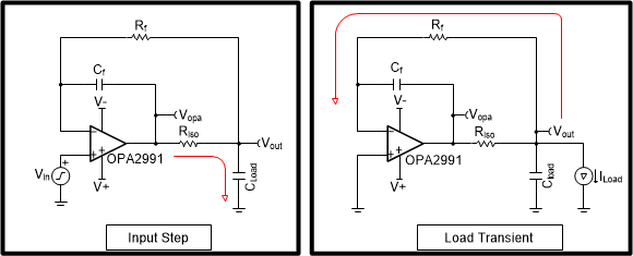 Figure 1-4 The dominate RC time constant
for input step (a) and output load (b) transients
Figure 1-4 The dominate RC time constant
for input step (a) and output load (b) transientsFigure 1-5 compares the input step and load transient output settling time (bottom responses) with the dominant RC time constants (top responses) described previously. Figure 1-5F(a) compares the input step settling time of Vout to an RC circuit response with a 100-Ω resistor and 10-nF capacitor (Riso and Cload). Figure 1-5(b) compares the output transient settling time to an RC circuit response with a 100-kΩ resistor and 270-pF capacitor (Rf and Cf). The RC circuit rise times match the input step and load transient output settling response, confirming the theory.
 Figure 1-5 Input step (a) and output load
(b) transient settling times, with dominate RC time constants
Figure 1-5 Input step (a) and output load
(b) transient settling times, with dominate RC time constantsThe stability criteria for the Riso+DFB circuit is discussed and explains how to optimize the feedback ratios for better load transient settling times. First, the op amp must be stable driving the Riso+Cload combination as a unity-gain buffer. Second, the 1/Beta pole formed by Rf and Cf must be at least less than half the frequency of the zero from Riso and Cload.
- Phase margin of unity-gain buffer driving Riso x Cload: >45°
- Feedback ratio: (Rf x Cf)/(Riso x Cload) > 2
For a greater explanation of the stability theory, see the TI Precision Labs Videos on Op Amp Stability.
While the minimum ratio of the feedback paths for stable operation is 2, there is not a maximum ratio for a stable circuit. Feedback-path ratios of 10, 100 or even 1,000 will also be stable with similar phase-margin results, provided that you meet the first criterion. However, as shown in Figure 1-5, the output load response is based on the time constant formed from the Rf and Cf components. Therefore, while stable, larger ratios will suffer from load responses that are much slower than the input response.
Figure 1-6 displays how the output settling response changes by altering the ratio of (Rf x Cf)/(Riso x Cload). When the feedback ratio is close to the minimum criterion of 2, the output responses for an input step and output load transient are nearly equivalent at the expense of some increasing overshoot and ringing. Increasing the ratio of (Rf x Cf)/(Riso x Cload) produces a more damped output that begins to have minimal impact for the input step response once the ratio is >20. Larger ratios continue increasing the load transient output response time, however, because of the ratio’s dominance on the Rf x Cf time constant.
 Figure 1-6 Output settling response for
multiple ratios for input step (top) and output load (bottom) transients
Figure 1-6 Output settling response for
multiple ratios for input step (top) and output load (bottom) transientsTherefore, for the best performance when responding to output load transients, you should design this circuit with a ratio of (Rf x Cf)/(Riso x Cload) close to 2. More conservative design approaches set this ratio between 4 and 10, knowing that interactions between the op-amp characteristics and circuit components and variations will result in some combinations lower than the targeted ratio. A ratio of the feedback components that falls below 2 will compromise the circuit’s stability.
A practical example where this effect comes into play is in ADC reference drive circuitry, as shown in Figure 1-7.
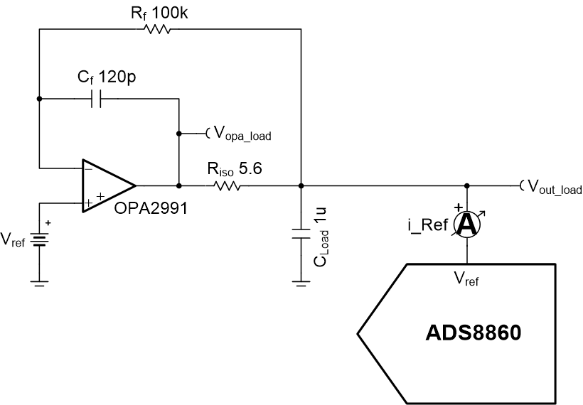 Figure 1-7 ADC reference drive
circuitry
Figure 1-7 ADC reference drive
circuitryDuring the conversion phases of the ADC, the successive approximation process includes switching internal capacitor digital-to-analog converter (CDAC) banks into the circuit. Each time a new capacitor switches into the circuit, a burst of current required from the external drive circuit will appear as a load transient. As a result, the Riso+DFB circuit may not properly settle to the load responses without proper configuration of the circuit feedback ratio.
Figure 1-8 shows these effects in the circuit simulations, using the op-amp circuit in Figure 1-7 as the reference buffer for the ADS8860, a 16-bit successive approximation register ADC configured to sample at 100 kSPS in this example. Varying the feedback path ratio in the circuit from values of roughly 3.6 to 360 displays the differences in load settling time. As expected from the results in Figure 1-5, the circuits with higher ratios take much longer for the reference buffer circuit to reach an equilibrium that results in a least significant bit settling error of <1/2 between conversions.
To illustrate this point, the lowest simulated ratio – 3.6 in Figure 1-8(a) – takes about four samples to reach equilibrium, while the results in Figure 1-8(c) with a ratio of 360 take over 400 samples, or about 4 ms, before the circuit reaches equilibrium. Applications commonly take bursts of samples with breaks between, and a circuit with the results shown in Figure 1-8(c) may never fully reach equilibrium before the burst of samples finishes. The unsettled reference can result in conversion errors and AC performance degradation. Recall that the phase margins and input responses of the circuits with ratios of 3.6 and 360 are nearly identical; unexpected circuit results may arise if you don’t design the circuit properly and verify the output load response.
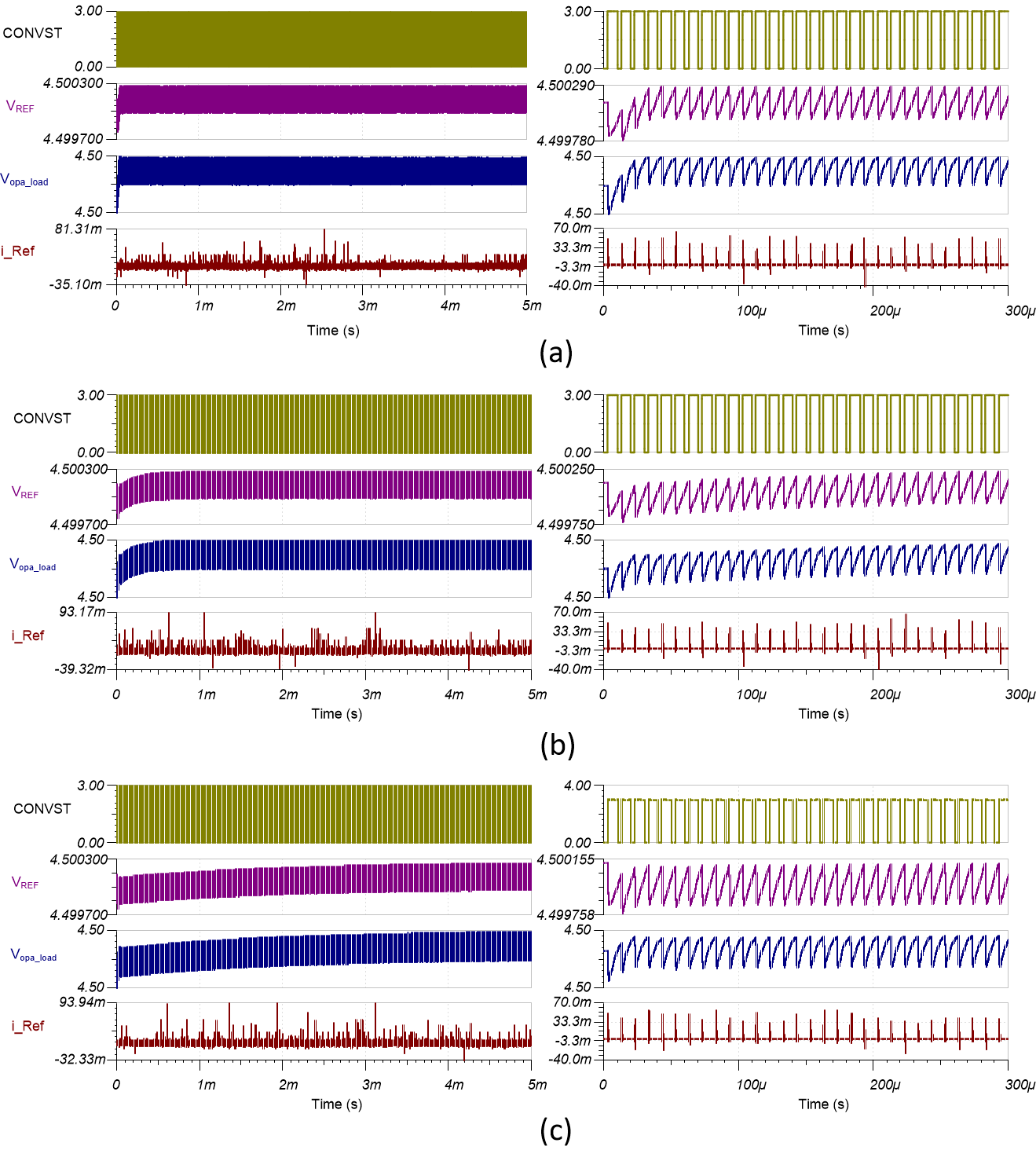 Figure 1-8 ADC reference drive settling
with different feedback ratios: 3.6 (a); 36 (b); and 360 (c). The left- and
right-hand graphs show 5-ms time scales and 300-µs time scales, respectively, of
the same results.