-
HD3SS460 4 x 6 Channels USB Type-C Alternate Mode MUX
- 1 Features
- 2 Applications
- 3 Description
- 4 Revision History
- 5 Device Comparison Table
- 6 Pin Configuration and Functions
- 7 Specifications
- 8 Detailed Description
- 9 Application and Implementation
- 10Power Supply Recommendations
- 11Layout
- 12Device and Documentation Support
- 13Mechanical, Packaging, and Orderable Information
- IMPORTANT NOTICE
HD3SS460 4 x 6 Channels USB Type-C Alternate Mode MUX
1 Features
- Provides MUX Solution for USB Type-CTM Ecosystem Including Alternate Mode (AM)
- Provides Wide Channel Selection Choices Including USBSS and 2 Ch AM, 4 Ch AM
- Compatible with 5 Gbps USB3.1 Gen 1 and AM Including 5.4 Gbps DisplayPort 1.2a
- Compatible for Source/Host and Sink/Device Applications
- Provides Cross-point MUX for Low Speed SBU Pins
- Bidirectional "Mux/De-Mux" Differential Switch
- Supports Common Mode Voltage 0-2 V
- Low Power with 1-μA Shutdown and 0.6 mA Active
- Single Supply Voltage VCC of 3.3 V ±10%
- Industrial Temperature Range of –40 to 85°C
2 Applications
- Flippable USB Type-CTM Ecosystem
- Tablets, Laptops, Monitors, Phones
- USB Host and Devices
- Docking Stations
3 Description
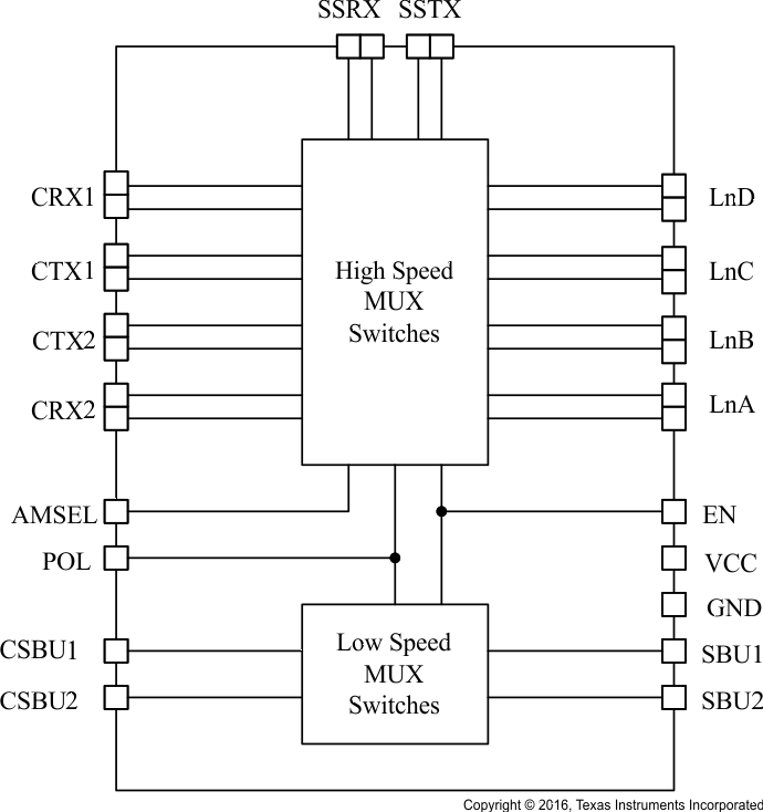
The HD3SS460 is a high-speed bi-directional passive switch in mux or demux configurations. Based on control pin POL the device provides switching to accommodate connector flipping. The device also provides muxing between 2Ch Data / 2Ch Video and all 4Ch Video based on control pin AMSEL.
The device also provides cross points MUX for low speed pins as needed in flippable connector implementation.
The HD3SS460 is a generic analog differential passive switch that can work for any high speed interface applications as long as it is biased at a common mode voltage range of 0-2V and has differential signaling with differential amplitude up to 1800mVpp. It employs an adaptive tracking that ensures the channel remains unchanged for entire common mode voltage range.
Excellent dynamic characteristics of the device allow high speed switching with minimum attenuation to the signal eye diagram with very little added jitter. It consumes <2 mW of power when operational and <5µW in shutdown mode, exercisable by EN pin.
Device Information(1)
| PART NUMBER | PACKAGE | BODY SIZE (NOM) |
|---|---|---|
| HD3SS460 | QFN (RHR) (28) | 3.50 mm × 5.50 mm |
| HD3SS460I | ||
| HD3SS460 | QFN (RNH) (30) | 2.50 mm × 4.50 mm |
| HD3SS460I |
- For all available packages, see the orderable addendum at the end of the data sheet.
sp
Simplified Schematic

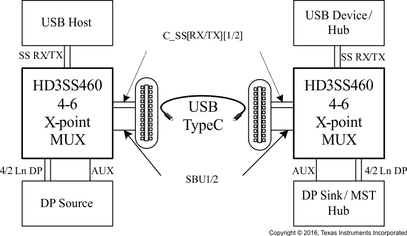
Application

4 Revision History
Changes from C Revision (December 2016) to D Revision
Changes from B Revision (June 2016) to C Revision
- Added QFN (RNH) (30) to the Device Information tableGo
- Added the RNH package option to the Device Comparison Table tableGo
- Added the RNH package option to the Pin Configuration and Functions sectionGo
- Changed the Description of pins LnBn, p, LnCn, p, LnDn, p, SSTXn, p, and SSRXn, p From: positive, negative To: negative, positive in the Pin Functions tableGo
- Changed the Supply voltage MIN value From: 3.0 V To: 2.7 V in the Recommended Operating Conditions tableGo
- Added the RNH package option to the Thermal Information table Go
- Changed VIH to include a separate line entry for POL pin in the Electrical Characteristics tableGo
Changes from A Revision (March 2015) to B Revision
- Changed text and Figure 3, Figure 4 in the USB SS and DP as Alternate Mode section for clarity. Go
- Added Figure 5Go
- Added Figure 6Go
- Deleted Table Pin Assignments for DP Source Pins and DP Sink Pins in the Detailed Design Procedure sectionGo
- Added Table 2, Table 3, Table 4, and Table 5 Go
- Added Figure 8 through Figure 13 Go
- Changed image for Figure 16 Go
- Changed image for Figure 19.Go
Changes from * Revision (January 2015) to A Revision
- Added full data sheet specification complement Go
5 Device Comparison Table(1)
| OPERATING TEMPERATURE (°C) | PART NUMBER | PINS | TOP-SIDE MARKING |
|---|---|---|---|
| 0 to 70 | HD3SS460RHR | 28 | 3SS460 |
| –40 to 85 | HD3SS460IRHR | 28 | 3SS460I |
| 0 to 70 | HD3SS460RNH | 30 | 460RNH |
| –40 to 85 | HD3SS460IRNH | 30 | 460IRNH |
6 Pin Configuration and Functions


Pin Functions
| PIN | TYPE(1) | DESCRIPTION | ||
|---|---|---|---|---|
| NAME | RHR NO. |
RNH NO. |
||
| VCC | 22 | 23 | P | Power |
| GND | PAD | 13, 28, PAD | G | Ground |
| POL | 3 | 3 | Input | Provides MUX control (Table 1) |
| AMSEL | 8 | 8 | 3-Level Input | Provides MUX configurations (Table 1) |
| EN | 17 | 18 | 3-Level Input | Enable signal; also provides MUX control (Table 1) |
| CRX1p, n | 1, 2 | 1, 2 | I/O | High Speed Signal Port CRX1 positive, negative |
| CTX1p, n | 4, 5 | 4, 5 | I/O | High Speed Signal Port CTX1 positive, negative |
| CTX2p, n | 6, 7 | 6, 7 | I/O | High Speed Signal Port CTX2 positive, negative |
| CRX2p, n | 9, 10 | 9, 10 | I/O | High Speed Signal Port CRX2 positive, negative |
| LnAn, p | 15, 16 | 16, 17 | I/O | High Speed Signal Port LnA positive, negative |
| LnBn, p | 18, 19 | 19, 20 | I/O | High Speed Signal Port LnB negative, positive |
| LnCn, p | 20, 21 | 21, 22 | I/O | High Speed Signal Port LnC negative, positive |
| LnDn, p | 23, 24 | 24, 25 | I/O | High Speed Signal Port LnD negative, positive |
| SSTXn, p | 25, 26 | 26, 27 | I/O | High Speed Signal Port SSTX negative, positive |
| SSRXn, p | 27, 28 | 29, 30 | I/O | High Speed Signal Port SSRX negative, positive |
| CSBU1, 2 | 11, 12 | 11, 12 | I/O | Low Speed Signal Port CSBU 1, 2 |
| SBU1, 2 | 13, 14 | 14, 15 | I/O | Low Speed Signal Port SBU 1, 2 |