SLLA561 May 2021 ISOW1044 , ISOW1412 , ISOW1432 , ISOW7740 , ISOW7741 , ISOW7742 , ISOW7743 , ISOW7744
1 TI Tech Note
Digital Isolator with Integrated DC/DC Converter
The ISOW7741 is a digital isolator that integrates an isolated DC/DC converter including a power transformer into a single SOIC package, as shown in Figure 1-1. The integrated DC/DC converter generates the isolated power to the secondary (isolated) side of device. Integration of the isolated DC/DC converter along with the power transformer into a single package makes the device a very compact solution. It also significantly reduces the complexity involved in designing the overall power supply compared to a discrete solution. Such devices are widely used in many industrial applications some of which include PLCs, communication modules, industrial transport, medical instruments, and energy meters.
The DC/DC converter in ISOW7741 switches at about 25 MHz to reduce the size of the power transformer and enable integration in a small SOIC package. At this switching frequency, the spectral components of the switching converter fall into a spectrum that may be subjected to regulatory restrictions by some electromagnetic interference (EMI) standards like CISPR 32.
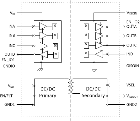 Figure 1-1 ISOW7741 Internal Block
Diagram
Figure 1-1 ISOW7741 Internal Block
DiagramCISPR 32 Emissions Standard Overview
CISPR 32 is an international radio disturbance standard for multimedia equipment (MME). The standard establishes requirements that provide an adequate level of protection for the radio spectrum and specifies procedures to ensure the reproducibility of measurement and the repeatability of results. Most industrial end-equipment certification agencies require the compliance of the end-equipment to CISPR 32 as one of the requirements for the end-equipment to be certified to the relevant end-equipment standard. Hence, it is critical for the product designers to consider these EMC requirements while designing their products.
The standard defines two classes of equipment associated with two types of end-user environments.
- Class B requirements are intended to offer adequate protection to broadcast services within the residential environment. Equipment intended primarily for use in a residential environment shall meet the Class B limits.
- Class A requirements are for all non-Class B equipment; Class A equipment shall comply with the more relaxed Class A limits.
PCB Layout Design Guidelines to Meet CISPR 32
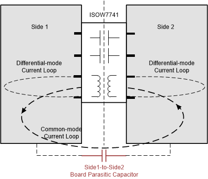 Figure 1-2 Common-Mode and
Differential-Mode Current Loops Formation With ISOW7741 on PCB
Figure 1-2 Common-Mode and
Differential-Mode Current Loops Formation With ISOW7741 on PCBElectromagnetic radiations can emit from a switching isolator on a given PCB in the form of either common-mode current loop or differential-mode current loop as shown in Figure 1-2. Minimize these radiations with careful PCB design and selection of the right components. A description of some of these methods follows:
- Decoupling Capacitors
Decoupling capacitors play an important role in filtering differential noise and keeping the voltage ripple to minimal. These capacitors also provide the instantaneous peak currents needed by various functional blocks in the DC/DC converter of ISOW7741. The capacitors are only effective when their values are carefully chosen to suit the switching frequency of the converter. The ISOW7741 requires a 0.01-µF capacitor is placed within 1-mm distance from the DC/DC converter supply pins (VDD/GND1 and VISOOUT/GND2). It is best to use a capacitor with the lowest equivalent series resistance (ESR) for frequencies from 10 MHz to 100 MHz. The ISOW7741 also requires a bulk capacitor of at least 10 µF is placed at 2–4 mm from the 0.01-µF capacitor. Use an optional 1-µF capacitor just before the 10 µF for better noise filtering. The 2- to 4-mm spacing between the 0.01-µF capacitor and bulk capacitors facilitates creation of equivalent series inductance (ESL) between them thereby creating a differential -filter. These three capacitors of different values, together, filter out the switching noise over a large band of frequencies.
The digital isolator part of ISOW7741 (VIO/GNDIO and VISOIN/GISOIN), like any other digital isolator, only requires a 0.1-µF decoupling capacitor on its supply pins. Any additional capacitors can be helpful but are optional. All these capacitors, collectively, minimize the differential radiations from the switching converter.
Important: place all these capacitors on the same PCB layer as the ISOW7741 device. Figure 1-3 shows an example PCB layout with the suggested decoupling capacitor placements.
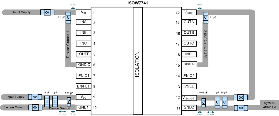 Figure 1-3 Example PCB ISOW7741
Layout
 - Ferrite Beads
The primary and secondary windings of the transformer in ISOW7741 are very close to each other inside the package, hence, a parasitic capacitance is formed between those windings. Fast switching currents in the DC/DC converter couple through this parasitic capacitance creating a common-mode current between side 1 and side 2 of the isolated system. Because the two sides are completely isolated, the current forms a large return loop through PCB-level parasitic capacitances, as shown in Figure 1-2. This large current loop can cause radiated emissions in isolated systems. Another way to understand the emissions mechanism is that the two isolated parts of the board form a dipole antenna transmitter. Large PCB sizes might create large current loops and such large current loops may cause higher radiations which can then be picked up by nearby systems in actual end-use and by the radiation measuring antenna during radiation compliance tests.
Ferrite beads (FB) are vital in minimizing radiated emissions due to common-mode current loops. FBs can be inserted between the ISOW7741 DC/DC converter and rest of the system, as Figure 1-3 shows, thereby breaking the path of larger common-mode current loops, and limiting formation of only shorter current loops. Such FBs in the path offer high attenuation to select frequencies thereby blocking the switching noise. Choose these FBs such that they offer the highest impedance (> 1 kΩ) at the switching frequency and its harmonic frequencies.
- Keep-Out Zones (KOZ)
As discussed in Ferrite Beads, FBs attenuate and block formation of large common-mode current loops. While FBs separate out the device from the rest of the PCB, ensure all the power and ground planes before and after FBs stay separated all through the PCB. Make sure this separation space in planes before and after FB is greater than the length of the FB. This ensures there are no alternate common-mode current loops formed which are created through capacitive coupling between the planes, bypassing FBs, if there was not enough separation. The best-case scenario is to completely avoid creation of any power or ground planes directly on device pins inside of FBs. Figure 1-4 highlights the keep-out zones that separate inner and outer planes with a good amount of space between them.
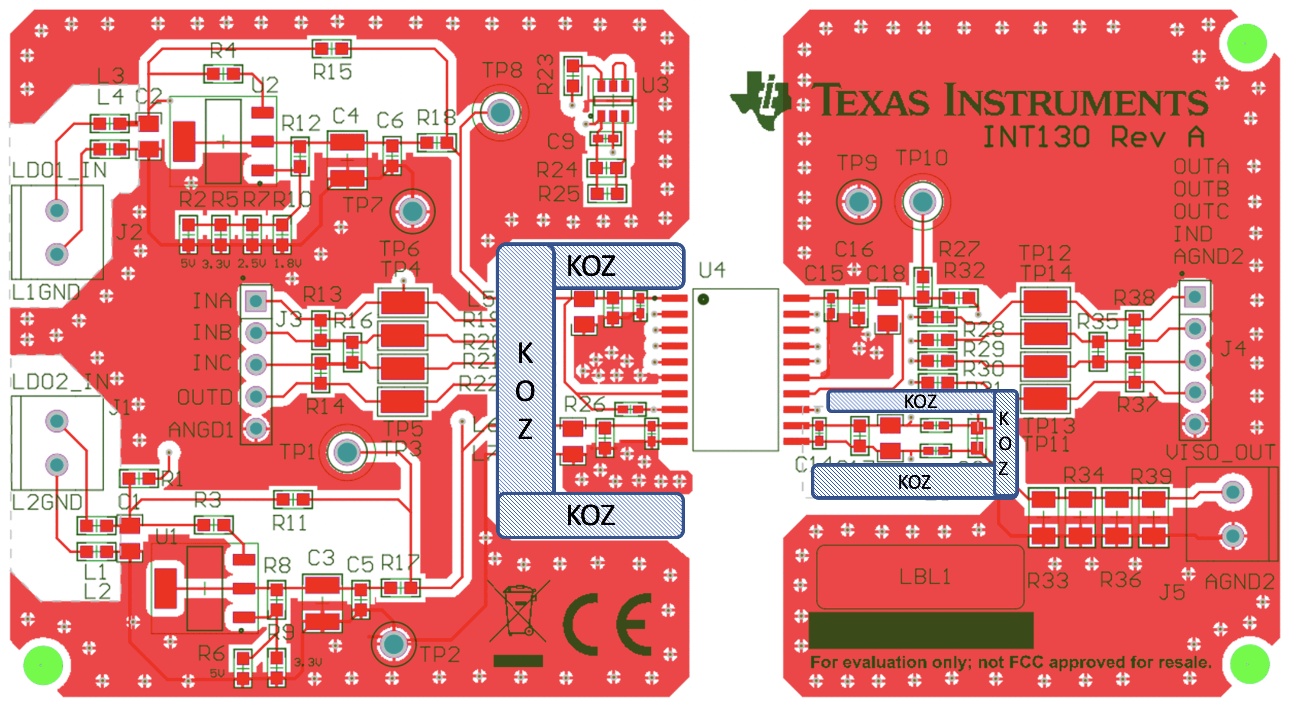 Figure 1-4 Keep-Out Zones (KOZ)
Highlighted in ISOW7741DFMEVM PCB Layout
Radiated Emissions Testing Guidelines
The primary reason for radiations is the formation of antennae on the board. Long cables used to power up the system or probes used to measure any parameter can act like antennae and cause a higher emission reading. It is important to make sure the setup used for emissions closely mimics the final system conditions in which it operates. Achieve this by keeping the cables connected to and originating from the system as short as possible or according to the actual system usage conditions. Any direct or capacitive connections of the board or metal shields to protected earth (PE) that are eventually planned for use in the final system must be present during EMI testing as well.
If the supply connections are long wires coming from a power supply placed far away from the DUT, then common-mode chokes (CMC) are recommended near the DUT so that the emissions are not unnecessarily aggravated by the long wires. In place of CMCs, use ferrite core clamp filters on the cables to minimize their impact on emissions measurement. By using these filters, emissions of the actual setup are measured, and the effect of the long cables is nullified. Solder any extra components required on the board, such as load resistors, directly to the board rather than connecting them to the board using long wires.
Another way to avoid such long wires is to power equipment under test (EUT) using batteries with very short wires if the EUT is DC powered. Figure 1-5 shows the evaluation module ISOW7741DFMEVM powered using a 9-V alkaline battery with very short connecting wires.
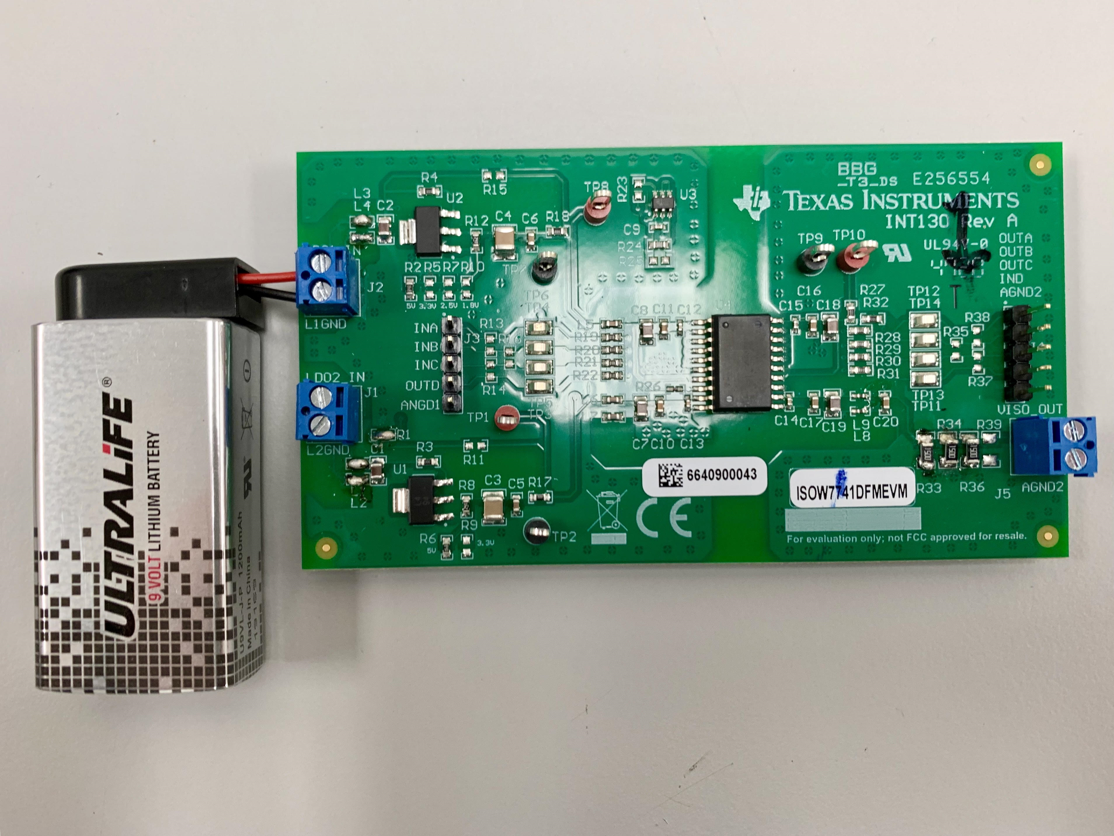 Figure 1-5 ISOW7741DFMEVM Emissions Test
Setup Using a Battery
Figure 1-5 ISOW7741DFMEVM Emissions Test
Setup Using a BatteryAccording to the CISPR 32 standard, the radiated emissions limits are specified as quasi-peak limits, although the peak-detector measurement is typically used to get a quick result. The device ISOW7741 uses clock dithering to change the switching frequency across a small band of frequencies instead of concentrating all the power at one single frequency. Techniques such as this show significantly better results when subjected to quasi-peak scans.
It is recommended to take peak-detector measurements first to find out the frequencies for the worst-case measurements Follow this with the quasi-peak measurements at the select worst-case frequencies to estimate the true margin from the CISPR 32 quasi-peak limit line.
Radiated Emissions Test Results
Figure 1-6 presents ISOW7741DFMEVM CISPR 32 test result with the test setup shown in Figure 1-5 for the voltage configuration of 5-V input, 5-V output with 100-mA load on VISOOUT and Figure 1-7 presents the result for the same test setup shown in Figure 1-5 for 3.3-V input, 3.3-V output with 50-mA load on VISOOUT. This shows that the ISOW7741 radiated emissions do not rise much above the ambient noise levels and the results comfortably meet CISPR 32 Class B limits, even with peak emissions measurements.
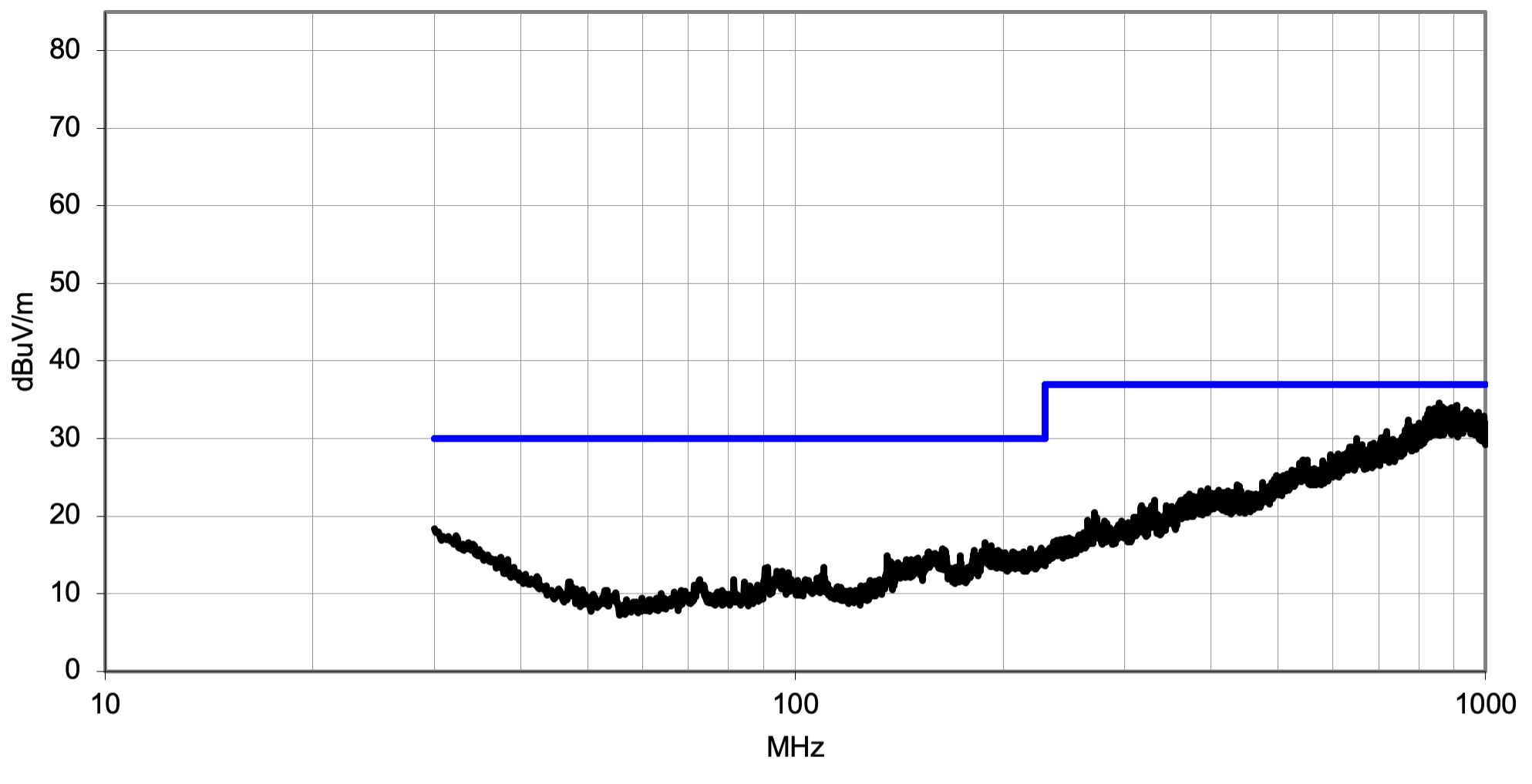 Figure 1-6 Radiated Emissions Result With
5-V Input, 5-V Output, 100-mA Load
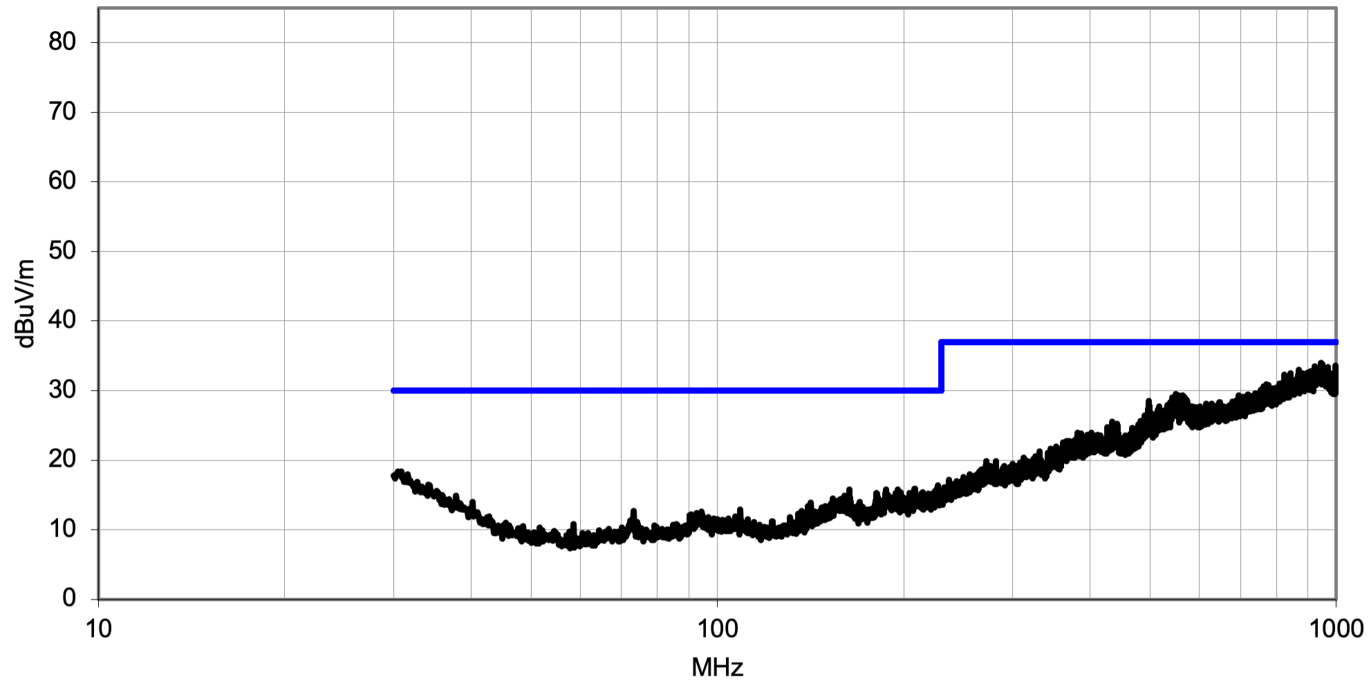 Figure 1-7 Radiated Emissions Result With
3.3-V Input, 3.3-V Output, 50-mA Load
Figure 1-7 Radiated Emissions Result With
3.3-V Input, 3.3-V Output, 50-mA LoadConclusion
Digital isolators with integrated DC/DC converters, like ISOW7741, have switching frequencies of the converters in the MHz range to keep the size of the transformer small. This high-frequency switching can cause radiated emissions of the integrated device to appear in the band of CISPR 32 frequency spectrum. Large PCBs and long connected cables aggravate the overall radiations of the DC/DC converter integrated isolated power solutions. The ISOW7741 has optimized radiated emissions performance due to the patented symmetric design architecture and clock dithering. Achieve further improvements in emissions by following the placement guidelines for suggested decoupling capacitors and ferrite beads and by maintaining suggested keep-out zones. These recommendations reduce the impact of large PCBs and long cables on radiated emissions results and enable the end-equipment to comply to CISPR 32 standard emissions limits.