SBOT037C March 2021 – March 2021 INA117 , INA188 , INA333 , INA592 , INA597 , INA826 , INA826S , OPA140 , OPA180 , OPA187 , OPA188 , OPA189 , OPA191 , OPA192 , OPA197 , OPA206 , OPA2140 , OPA2180 , OPA2187 , OPA2188 , OPA2189 , OPA2191 , OPA2192 , OPA2197 , OPA2205 , OPA2206 , OPA2330 , OPA2333 , OPA2376 , OPA277 , OPA330 , OPA333 , OPA334 , OPA335 , OPA376 , OPA378 , OPA388 , OPA391 , OPA396 , OPA4140 , OPA4180 , OPA4187 , OPA4188 , OPA4191 , OPA4192 , OPA4197 , OPA4205 , OPA4330 , OPA4376 , OPA734 , OPA735 , OPA827 , TLV2376 , TLV333 , TLV376 , TLV4376
1 Overview of Offset Correction Methods
Introduction
Amplifier input offset voltage is often the key parameter for design accuracy, and there are different circuit techniques used to minimize it. Knowing the various trimming and offset correction methods may be productive when selecting an amplifier for a particular application.
Laser trim: Wafer-Level Trim
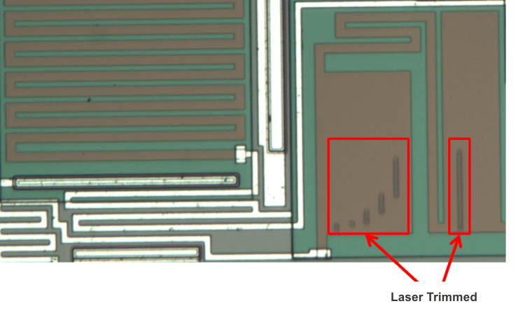
Each amplifier is composed of tens to thousands of transistors, resistors, and capacitors. The device input offset error is caused by the mismatch (or variations) of the input transistors in each amplifier. Figure 1-1 shows a photo of an op amp die. The highlighted areas show the thin film resistors. During the wafer-level test process, a laser burns away sections of resistive material, thus adjusting its value by increasing the total resistance of the die.
 Figure 1-1 Laser Trimming on Thin-Film
Resistors
Figure 1-1 Laser Trimming on Thin-Film
ResistorsThis trimming can actually be done while the device is in operation under the laser; that is, we can monitor the offset voltage and then trim the resistor until the offset is nulled to zero. Wafer-level trimming may produce very accurate results. However, after the wafer is sawn into individual dies and packaged, any physical stress to a given die can produce some shifts in the offset voltage.
Laser trim is a practical way to trim ICs fabricated on a bipolar wafer process. It is used widely not only for op amps, but also in difference and instrumentation amplifiers to improve the resistor matching that is critical in minimizing gain error while optimizing common-mode rejection ratio (CMRR) performance. The INA826S is an instrumentation amplifier that uses laser trim to achieve high DC accuracies and low quiescent current: 150-µV offset, 2-µV/°C drift, and 250-µA quiescent current. With the additional shutdown function and small (3-mm × 3-mm) DFN package, this amplifier is suitable for power-sensitive applications such as circuit breakers, portable medical instrumentation, and test equipment.
e-Trim™: Package-Level Trim
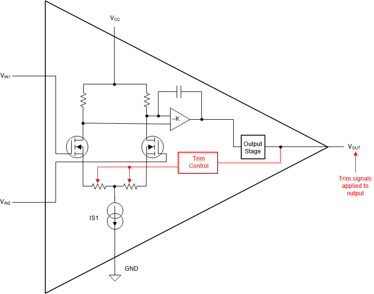
Another method used to achieve low offset voltage and drift is e-Trim, which is TI’s patented trimming architecture implemented after device packaging. Correction current sources internal to the devices are adjusted during the final package-level manufacturing test. Once the trimming is completed, the gateway to trim circuitry is closed, so the trim control circuit is disabled and the adjustments become permanent. Figure 1-2 illustrates the e-Trim method.
This polysilicon, fuse-blowing technique does not require extra pins or test pads and provides substantial improved performance over wafer-level trim. This approach also avoids the parameter shifts that typically occur as a result of package stress, producing the excellent precision only possible with zero-drift amplifiers and allowing miniature package sizes.
 Figure 1-2 Package-Level e-Trim
The OPA2191 is the newest addition to the e-Trim amplifier family, featuring 25-µV (max) offset voltage, 0.8-µV/°C (max) drift, and low quiescent current of 200 µA per amplifier.
Chopper: Dynamic Correction
Although it is not a trim method as such, a third method to correct offset and drift is with a zero-drift amplifier. The chopper is a common type of zero-drift amplifier that uses an internal dynamic calibration method to minimize the offset voltage. Figure 1-3 shows the diagram of a typical chopper architecture. The input and output of the first trans-conductance stage has a set of switches that swaps the polarity of the input signal once every calibration cycle. The drift over time and temperature is averaged to zero. This characteristic also eliminates the 1/f noise that occurs in conventional amplifiers at very low frequencies. These features make chopper amplifiers very useful in DC (or low-frequency) signal conditioning applications such as weigh scales, strain gauges, and temperature measurement. The OPA2187 is an example of a chopper with 10-µV (max) offset voltage, 0.05-µV/°C (max) drift, and 0.4-µVPP low-frequency noise (0.1 Hz to 10 Hz), all with only 145-µA (max) quiescent current per amplifier.
 Figure 1-3 Typical Diagram of Chopper
Amplifier
Figure 1-3 Typical Diagram of Chopper
AmplifierChopper amplifiers, however, can insert an additional noise component caused by charge injection because of the switch closing and opening; these operations induce spikes in the input bias current that may be converted into voltage spikes in high source impedance applications or during use of high-value resistors to gain up the signal. For this reason, in applications with a narrow temperature range such as medical instrumentation, the near-zero drift may not be as important as the ultra-low input bias current of the amplifier coupled with high source impedance. In such cases, the OPA2191 with 20-pA (max) bias current is likely a better option than the OPA2187 with much lower offset drift but 350-pA (max) bias current.
Summary
Table 1-1 compares the three offset correction methods. This technical brief may serve as a guide to help you select an amplifier that best meets your low-offset, low-drift circuit needs.
| Devices | Correction Method | Advantages | Disadvantages |
|---|---|---|---|
| INA826S OPA145 OPA2325 |
Laser trim | Simplified manufacturing flow over temperature | Parameter shifts after packaging |
| OPA391 OPA392OPA2191 OPA2192 OPA2376 OPA2205 OPA2206 |
e-Trim | No parameter shifts because of packaging | Complex manufacturing flow over temperature |
| INA188 OPA189 OPA2182 OPA388 OPA2387 |
Chopper | Lowest possible drift; no 1/f noise | Bias current spikes can cause problems with high source impedances |
| Resources | Blog Post |
|---|---|
| Video | Op Amp Technology Overview |
| Precision Hub Blog | How does package level trim compare to other offset correction methods? |
| Precision Hub Blog | Trimmed or chopped: How do you like your op amp? |
| EDN Analog Design Post | Pushing the precision envelope – Understanding the precision challenge in operational amplifiers |