SBOA296 April 2021 OPA322 , OPA350 , TLV9062
Design Goals
| Input | Output | Frequency | Supply | |
|---|---|---|---|---|
| ViMax | VoMax | fMax | Vcc | Vee |
| 9Vpp | 4.5Vpp | 50kHz | 5V | 0V |
Design Description
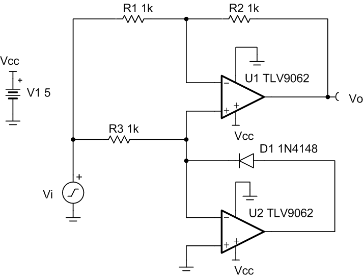
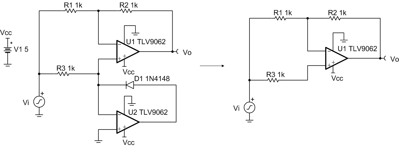
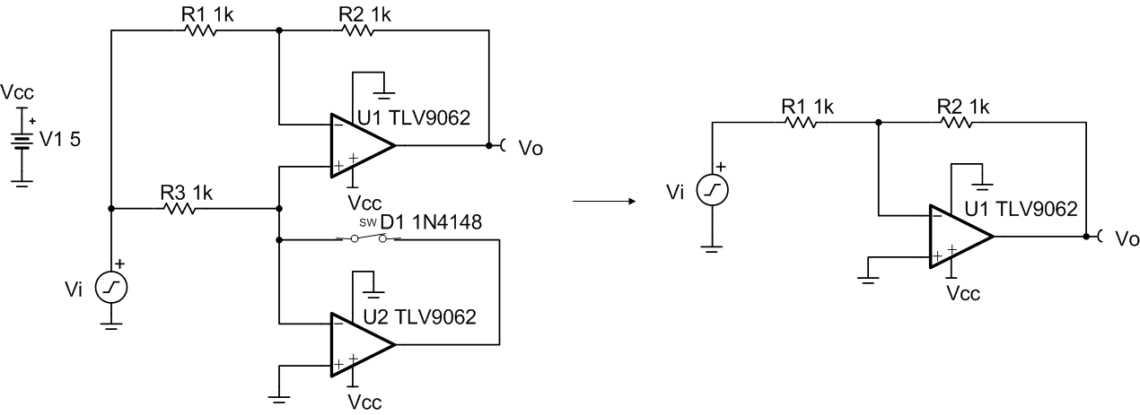
This single-supply precision full-wave rectifier is optimized for high-input voltages. When Vi > 0V, D1 is reverse biased and the top part of the circuit, U1, is activated resulting in a circuit with a gain of 1V/V. When Vi < 0V, D1 is forward biased and the bottom part of the circuit, U2, is activated resulting in an inverting amplifier circuit with a gain of –1V/V.
Design Notes
- Observe common-mode and output swing limitations of op amps.
- R3 should be sized small enough that the leakage current from D1 does not cause errors for positive input cycles while ensuring the op amp can drive the load.
- Use a fast switching diode for D1.
- Resistor tolerance determines the gain error of the circuit.
- Use a negative charge pump (such as the LM7705) for output swing requirements to GND to maintain linearity for output signals near 0V. For additional information. see Single-supply, low-input voltage, full-wave rectifier circuit.
- For more information on op amp linear operating region, stability, capacitive load drive, driving ADCs, and bandwidth please see the Design References section.
Design Steps
- Circuit analysis for positive input signals. D1 is reverse-biased disconnecting the output of U2 from the non-inverting input of U1.
 Equation 1.Equation 1.
 - Circuit analysis for negative input signals. D1 is forward biased, which connects the output of U2 to the non-inverting input of U1, which is GND.
 Equation 1.Equation 1.
 - Select R1, R2, and R3. Equation 1.
Design Simulations
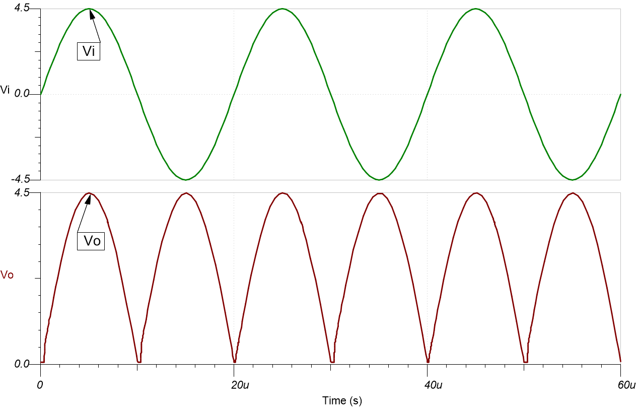
Transient Simulation Results
A 1-kHz, 9-Vpp sine wave yields a 4.5-Vpp output sine wave.

A 50-kHz, 9-Vpp sine wave yields a 4.5-Vpp output sine wave.
Design References
- See Analog Engineer's Circuit Cookbooks for the comprehensive TI circuit library.
- SPICE Simulation File SBOC529.
- TI Precision Labs
- See the Single-Supply Low-Input Voltage Optimized Precision Full-Wave Rectifier Reference Design.
Design Featured Op Amp
| TLV9062 | |
|---|---|
| Vss | 1.8V to 5.5V |
| VinCM | Rail–to–rail |
| Vout | Rail–to–rail |
| Vos | 0.30mV |
| Iq | 538µA |
| Ib | 0.5pA |
| UGBW | 10MHz |
| SR | 6.5V/µs |
| #Channels | 1, 2, 4 |
| www.ti.com/product/TLV9062 | |
Design Alternate Op Amps
| OPA322 | OPA350 | |
|---|---|---|
| Vss | 1.8V to 5.5V | 2.7V to 5.5V |
| VinCM | Rail–to–rail | Rail–to–rail |
| Vout | Rail–to–rail | Rail–to–rail |
| Vos | 2mV | 0.15mV |
| Iq | 1.9mA | 5.2mA |
| Ib | 10pA | 0.5pA |
| UGBW | 20MHz | 38MHz |
| SR | 10V/µs | 22V/µs |
| #Channels | 1, 2, 4 | 1, 2, 4 |
| www.ti.com/product/OPA322 | www.ti.com/product/OPA350 |