SBOA284 March 2021 OPA375 , TLV9002
Design Goals
| Input | Output | BW | Supply | |||
|---|---|---|---|---|---|---|
| IiMin | IiMax | VoMin | VoMax | fp | Vcc | Vee |
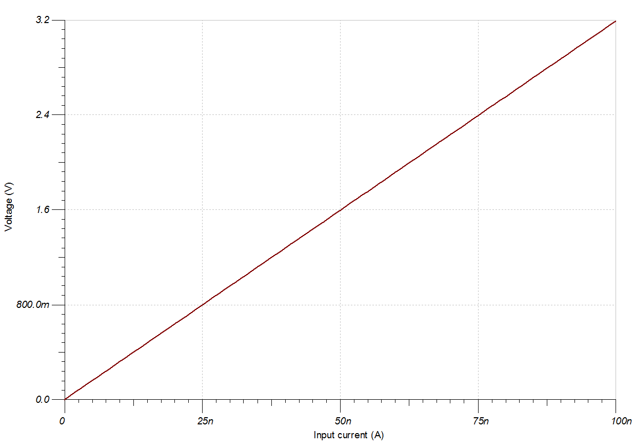
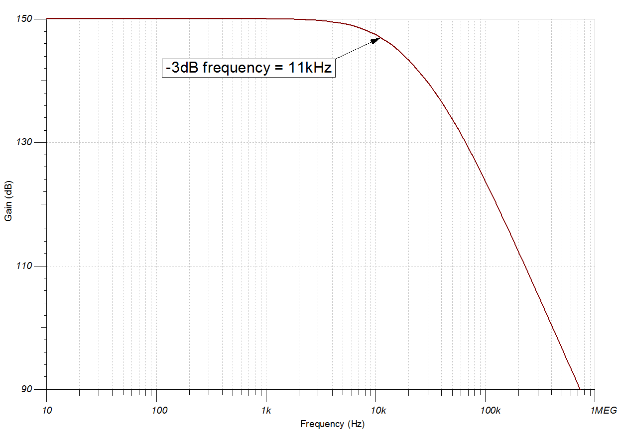
| 0A | 100nA | 0V | 3.2V | 10kHz | 3.3V | 0V |
Design Description
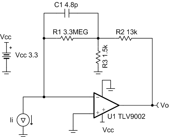
This transimpedance amplifier with a T-network feedback configuration converts an input current into an output voltage. The current-to-voltage gain is based on the T-network equivalent resistance which is larger than any of the resistors used in the circuit. Therefore, the T-network feedback configuration circuit allows for very high gain without the use of large resistors in the feedback or a second gain stage, reducing noise, stability issues, and errors in the system.
Design Notes
- C1 and R1 set the input signal cutoff frequency, fp.
- Capacitor C1 in parallel with R1 helps limit the bandwidth, reduce noise, and also improve the stability of the circuit if high-value resistors are used.
- The common-mode voltage is the voltage at the non-inverting input and does not vary with input current.
- A bias voltage can be added to the non-inverting input to bias the output voltage above the minimum output swing for 0A input current.
- Using high-value resistors can degrade the phase margin of the circuit and introduce additional noise in the circuit.
- Avoid placing capacitive loads directly on the output of the amplifier to minimize stability issues.
- For more information on op amp linear operating region, stability, slew-induced distortion, capacitive load drive, driving ADCs, and bandwidth see the Design References section.
Design Steps
The transfer function of this circuit follows:
- Calculate the required gain: Equation 1.
- Choose the resistor values to set the pass-band gain: Equation 1.
Since R1 will be the largest resistor value in the system choose this value first then choose R2 and calculate R3. Select R1 = 3.3MΩ and R2 = 13kΩ. R1 is very large due to the large transimpedance gain of the circuit. R2 is in the ~10k ohm range so the op amp can drive it easily.
Equation 1. - Calculate C1 to set the location of fp. Equation 1.
- Run a stability analysis to make sure that the circuit is stable. For more information on how to run a stability analysis see the TI Precision Labs - Op amp: Stability video.
Design Simulations
DC Simulation Results
AC Simulation Results
Design References
- See Analog Engineer's Circuit Cookbooks for TI's comprehensive circuit library.
- See SPICE file, SBOMB39.
- See TIPD176, www.ti.com/tool/tipd176.
- For more information on many op amp topics including common-mode range, output swing, bandwidth, and how to drive an ADC please visit TI Precision Labs.
Design Featured Op Amp
| TLV9002 | |
|---|---|
| Vcc | 1.8V to 5.5V |
| VinCM | Rail-to-rail |
| Vout | Rail–to–rail |
| Vos | 0.4mV |
| Iq | 60µA |
| Ib | 5pA |
| UGBW | 1MHz |
| SR | 2V/µs |
| #Channels | 1, 2, 4 |
| www.ti.com/product/TLV9002 | |
Design Alternate Op Amp
| OPA375 | |
|---|---|
| Vcc | 2.25V to 5.5V |
| VinCM | Vee to (Vcc –1.2V) |
| Vout | Rail–to–rail |
| Vos | 0.15mV |
| Iq | 890µA |
| Ib | 10pA |
| UGBW | 10MHz |
| SR | 4.75V/µs |
| #Channels | 1 |
| www.ti.com/product/OPA375 | |