SBOA272C December 2020 – January 2021 LMC7101 , OPA170
Design Goals
| Input 1 | Input 2 | Output | Freq. | Supply | ||||
|---|---|---|---|---|---|---|---|---|
| Vi1Min | Vi1Max | Vi2Min | Vi2Max | VoMin | VoMax | f | Vcc | Vee |
| –2.5V | 2.5V | –250mV | 250mV | –4.9V | 4.9V | 10kHz | 5V | –5V |
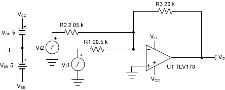
Design Description
This design sums (adds) and inverts two input signals, Vi1 and Vi2. The input signals typically come from low-impedance sources because the input impedance of this circuit is determined by the input resistors, R1 and R2. The common-mode voltage of an inverting amplifier is equal to the voltage connected to the non-inverting node, which is ground in this design.
Design Notes
- Use the op amp in a linear operating region. Linear output swing is usually specified under the AOL test conditions. The common-mode voltage in this circuit does not vary with input voltage.
- The input impedance is determined by the input resistors. Make sure these values are large when compared to the output impedance of the source.
- Using high-value resistors can degrade the phase margin of the circuit and introduce additional noise in the circuit.
- Avoid placing capacitive loads directly on the output of the amplifier to minimize stability issues.
- Small-signal bandwidth is determined by the noise gain (or non-inverting gain) and op amp gain-bandwidth product (GBP). Additional filtering can be accomplished by adding a capacitor in parallel to R3. Adding a capacitor in parallel with R3 will also improve stability of the circuit if high-value resistors are used.
- Large signal performance may be limited by slew rate. Therefore, check the maximum output swing versus frequency plot in the data sheet to minimize slew-induced distortion.
- For more information on op amp linear operating region, stability, slew-induced distortion, capacitive load drive, driving ADCs, and bandwidth please see the Design References section.
Design Steps
The transfer function for this circuit is given below.

- Select a reasonable resistance
value for R3. Equation 1.

- Calculate gain required for
Vi1. For this design, half of the output swing is devoted to
each input. Equation 1.

- Calculate the value of
R1. Equation 1.

- Calculate gain required for
Vi2. For this design, half of the output swing is devoted to
each input. Equation 1.

- Calculate the value of
R2. Equation 1.

- Calculate the small signal
circuit bandwidth to ensure it meets the 10-kHz requirement. Be sure to use
the noise gain (NG), or non-inverting gain, of the circuit. When calculating
the noise gain note that R1 and R2 are in parallel.
Equation 1.
 Equation 1.
 Equation 2.
- This requirement is met because the closed-loop bandwidth is 102kHz and the design goal is 10kHz.
- Calculate the minimum slew rate
to minimize slew-induced distortion. Equation 3.
 Equation 3.
- SROPA170=0.4V/µs, therefore it meets this requirement.
- To avoid stability issues
ensure that the zero created by the gain setting resistors and input
capacitance of the device is greater than the bandwidth of the circuit.
Equation 4.
 Equation 4.
 Equation 5.
- Ccm and Cdiff are the common-mode and differential input capacitances.
- Since the zero frequency is greater than the bandwidth of the circuit, this requirement is met.
Design Simulations
DC Simulation Results
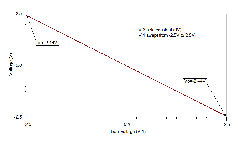
This simulation sweeps Vi1 from –2.5V to 2.5V while Vi2 is held constant at 0V. The output is inverted and ranges from –2.44V to 2.44V.
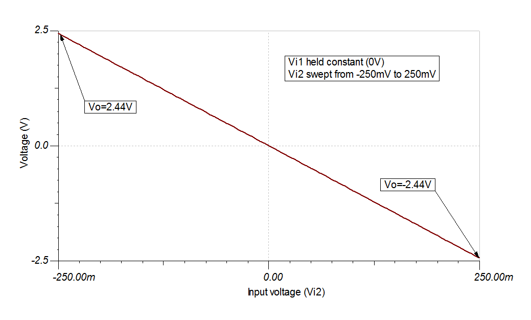
This simulation sweeps Vi2 from –250mV to 250mV while Vi1 is held constant at 0V. The output is inverted and ranges from –2.44V to 2.44V.
AC Simulation Results
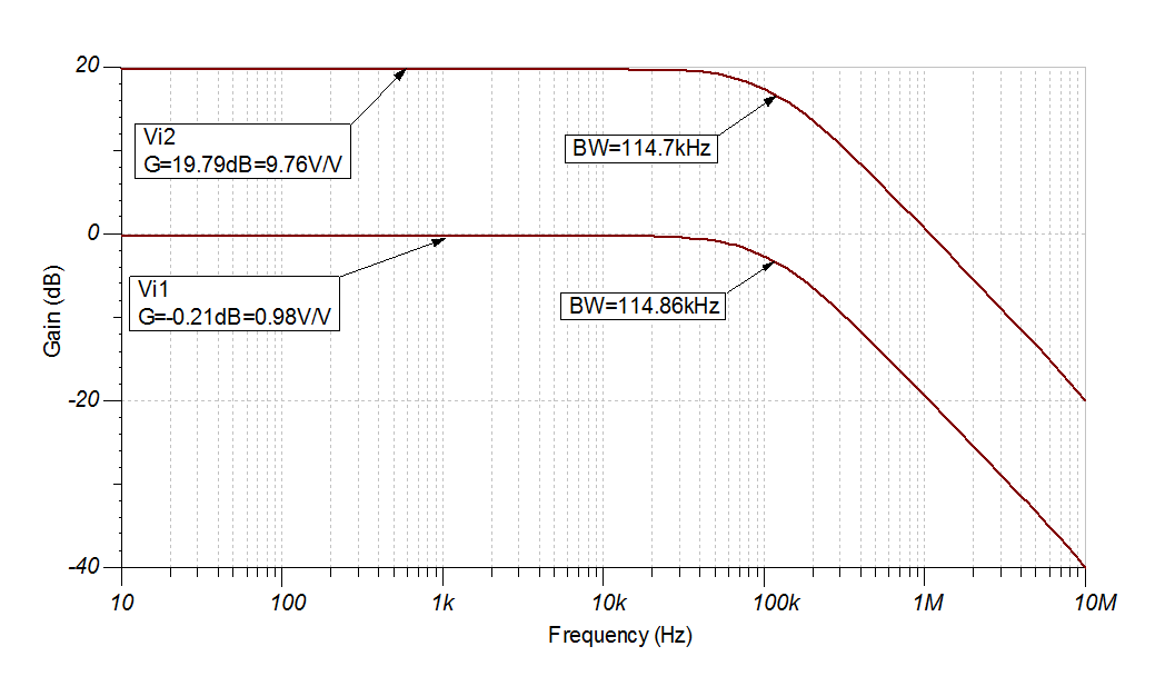
This simulation shows the bandwidth of the circuit. Note that the bandwidth is the same for either input. This is because the bandwidth depends on the noise gain of the circuit, not the signal gain of each input. These results correlate well with the calculations.
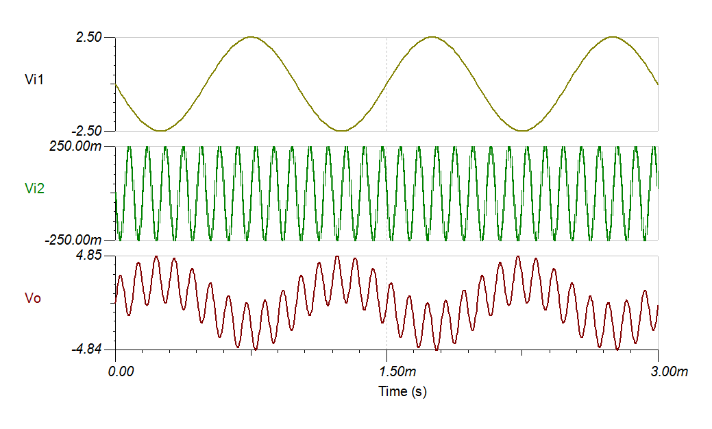
Transient Simulation Results
This simulation shows the inversion and summing of the two input signals. Vi1 is a 1-kHz, 5-Vpp sine wave and Vi2 is a 10-kHz, 500-mVpp sine wave. Since both inputs are properly amplified or attenuated, the output is within specification.
Design References
See Analog Engineer's Circuit Cookbooks for TI's comprehensive circuit library.
See circuit SPICE simulation file SBOC494.
For more information on many op amp topics including common-mode range, output swing, bandwidth, and how to drive an ADC please visit TI Precision Labs.
Design Featured Op Amp
| OPA170 | |
|---|---|
| Vss | 2.7V to 36V |
| VinCM | (Vee-0.1V) to (Vcc-2V) |
| Vout | Rail-to-rail |
| Vos | 0.25mV |
| Iq | 110µA |
| Ib | 8pA |
| UGBW | 1.2MHz |
| SR | 0.4V/µs |
| #Channels | 1, 2, 4 |
| www.ti.com/product/opa170 | |
Design Alternate Op Amp
| LMC7101 | |
|---|---|
| Vss | 2.7V to 15.5V |
| VinCM | Rail-to-rail |
| Vout | Rail-to-rail |
| Vos | 110µV |
| Iq | 0.8mA |
| Ib | 1pA |
| UGBW | 1.1MHz |
| SR | 1.1V/µs |
| #Channels | 1 |
| www.ti.com/product/lmc7101 | |
| Revision | Date | Change |
|---|---|---|
| C | January 2021 | Updated Formula format |
| B | December 2020 | Updated Design Goals Table |
| A | January 2019 | Down-style title. Updated title role to Amplifiers. Added link to circuit cookbook landing page. |