Simulating Electromagnetic Interference – Is It Possible?
John Rice
Today, gigahertz processors powered by high-frequency multi-phase DC/DC converters communicate with memory at gigahertz speeds. At these frequencies, component and printed circuit board (PCB) parasitic impedances create frequency dependent voltage drops, antenna structures and PCB resonances that in turn create electromagnetic interference (EMI), signal integrity and power integrity (SI/PI) issues. In a previous post, I examined the challenge of meeting electromagnetic compliance with ultrafast, power transistors like the LMG5200 half-bridge GaN switch. In this post, we’ll look at highly sophisticated soft tools that can help identify PCB problem areas before manufacturing.
Designing high-speed, mixed-signal PCBs requires highly experienced engineering personnel and equipment resources – As such, development cost can be very high especially when multiple iterations of a board are required to achieve compliance. EMI, SI and PI design issues delay product release and when uncovered after product release result in customer returns, product recalls and a loss in consumer confidence. The profitability of a company depends on careful analysis of their products and as operating frequency increases, so too does a need to understand the electromagnetic (EM) field behavior of PCBs.
Fortunately, the same high speed gigahertz processors and circuit boards have enabled a new paradigm in circuit design: highly advanced circuit simulation. As many already know, you can use circuit simulation to optimize circuit performance and even perform worst case circuit analysis of the known PCB devices. But, can you simulate the “hidden” PCB parasitic elements that are the source of EMI and SI/PI issues? Fortunately, the answer today is most definitely yes!
I’ve been watching the advancement of 3-D EM solvers for the past few years and I am very impressed with work done by Computer Simulation Technology (CST) for the purpose of 3-D EM analysis. For example, I quickly imported the LMG5200 evaluation board CAD files into CST EMC Studio as an OBD++ file, and characterized the PCB planes, traces and components impedance using a broadband excitation signal.
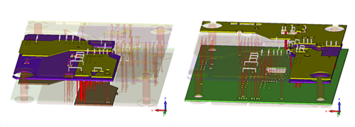
Careful examination of a board circuit board traces, plane structure, vias and component placement is an essential element in advancing any high-speed circuit board design. In CST EMC Studio, I found that the power ground was connected to a smaller split plane on layer two (Figure 1). When I applied the excitation to the solid ground plane shown instead of the split plane the simulated radiated emissions improved significantly. The result correlated well with results previously measured using a TEM cell, as I discussed in an earlier blog post.
 Figure 1 Layer Stack-up Visualization
in CST EMC Studio
Figure 1 Layer Stack-up Visualization
in CST EMC StudioThe illustration on the left of Figure 1 shows how the input “power ground” is connected to a split plane on layer two (the purple plane). The illustration on the right shows the ground plane (in green) on layer 3.
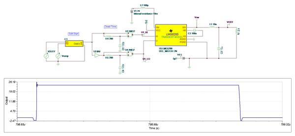
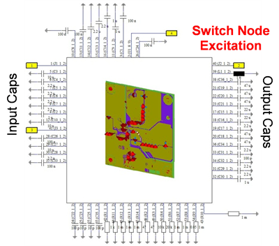
A SPICE circuit simulation of the LMG5200 in TINA-TI™ predicted the switching behavior of the LMG5200 of a 60W, 24V to 12V power conversion and is shown in Figure 2. This simulation could have also been done in CST Design Studio. This switching waveform was then applied to the 3-D EM simulation result in a “co-simulation” shown in Figure 3 using CST Design Studio. Beware however that 3-D EM simulation is computationally intensive – solving Maxwell’s equations in a complex circuit board mesh takes time! The 3-D EM simulation took over 3 hours to run on a quad core computer with a graphic processing unit and 8 GB of memory. The input/output capacitors and excitation signals are represented as ports inside CST Design Studio and the E-field result is shown in Figure 4.
 Figure 2 Excitation Signal for 3-D EM
Simulation
 Figure 3 Co-simulation – SPICE
Excitation into 3-D EM Field Simulation
 Figure 4 Sphere of Probes and E-field
Measurement at 3m
Figure 4 Sphere of Probes and E-field
Measurement at 3mThe simulation result in Figure 4 is a record of each E-field probe placed around board in a sphere of probes at 3-meters. Resonances at specific frequencies correlated well with measured results from my previous post. You can see from the result that probes at certain locations had higher levels of emissions, providing insight into potential problem areas on the board.
It is clear from this basic application of a powerful 3-D EM simulator that it is possible – and increasingly important – to simulate the microwave behavior of PCBs when attempting to design high-speed power converters, power distribution networks (PDN) and other high speed signal/communication buses. Circuit board designs using wide-bandgap semiconductors like the LMG5200 will have to deal with picosecond rise times and voltage slew rates of over 40V/ns. Power conversion like this necessitates higher sensitivities to EM field behavior when advancing solutions compliant with electromagnetic compatibility. Fortunately 3-D EM field solvers have advanced to help engineers isolate problems earlier in the design phase saving cost and accelerating product time to market.
Additional Resources: Get caught up with part one and two of John Rice’s series
IMPORTANT NOTICE AND DISCLAIMER
TI PROVIDES TECHNICAL AND RELIABILITY DATA (INCLUDING DATASHEETS), DESIGN RESOURCES (INCLUDING REFERENCE DESIGNS), APPLICATION OR OTHER DESIGN ADVICE, WEB TOOLS, SAFETY INFORMATION, AND OTHER RESOURCES “AS IS” AND WITH ALL FAULTS, AND DISCLAIMS ALL WARRANTIES, EXPRESS AND IMPLIED, INCLUDING WITHOUT LIMITATION ANY IMPLIED WARRANTIES OF MERCHANTABILITY, FITNESS FOR A PARTICULAR PURPOSE OR NON-INFRINGEMENT OF THIRD PARTY INTELLECTUAL PROPERTY RIGHTS.
These resources are intended for skilled developers designing with TI products. You are solely responsible for (1) selecting the appropriate TI products for your application, (2) designing, validating and testing your application, and (3) ensuring your application meets applicable standards, and any other safety, security, or other requirements. These resources are subject to change without notice. TI grants you permission to use these resources only for development of an application that uses the TI products described in the resource. Other reproduction and display of these resources is prohibited. No license is granted to any other TI intellectual property right or to any third party intellectual property right. TI disclaims responsibility for, and you will fully indemnify TI and its representatives against, any claims, damages, costs, losses, and liabilities arising out of your use of these resources.
TI’s products are provided subject to TI’s Terms of Sale (www.ti.com/legal/termsofsale.html) or other applicable terms available either on ti.com or provided in conjunction with such TI products. TI’s provision of these resources does not expand or otherwise alter TI’s applicable warranties or warranty disclaimers for TI products.
Mailing Address: Texas Instruments, Post Office Box 655303, Dallas, Texas 75265
Copyright © 2023, Texas Instruments Incorporated