-
GaN to the Rescue! Part 2: Measurements
GaN to the Rescue! Part 2: Measurements
Steve Widener
In my last post, I provided an introduction to body-diode reverse recovery. Now we will take a look at a method for measuring reverse recovery in an actual circuit.
Measuring reverse recovery in a synchronous buck converter is a challenge. Current probes are fairly large and would add significant inductance to the power-stage loop. The bandwidth of current probes is also inadequate.
How about a shunt resistor? That sounds promising, but you’ll need to make sure that it doesn’t introduce significant loop inductance. I found a few that are 10 mΩ and “low inductance.”
I’m tempted to put this in the source of the synchronous FET, but there are two problems:
- The shunt may see the gate-drive current as well as the recovery and load current.
- The shunt will add inductance that may affect the lower gate drive due to the high di/dt currents.
One solution is to put the shunt resistor in the drain of the upper MOSFET so that there is no chance of it interfering with the gate drives. The Vishay VCS1625/Y08500R01000F9R worked – it is built with Kelvin connections and constructed to reduce inductance. Fore more information, see Figure 1.
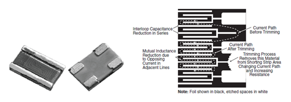 Figure 1 Shunt Resistor
Silicon MOSFET Recovery Measurement
To get a baseline Qrr measurement with a silicon MOSFET bridge, I got out a cutting knife, cut an island for the shunt resistor on the TPS40170EVM-597, and placed the shunt resistor. I used a 50Ω SMA-to-BNC cable to run the signal to the scope (terminated with 50Ω). I placed a 50Ω resistor in series so I get one-half the signal, but no ringing. Be sure to use skew adjustments when mixing probe types!
Note that with the shunt in the top, the scope is grounded to the positive input rail. This means that the power-supply positive output is grounded (negative supply to the buck converter) and any other test equipment like load banks must not short out the supplies through the scope connections. Figure 2 shows the modified evaluation module (EVM) schematic.
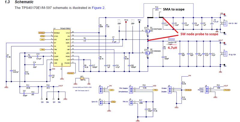 Figure 2
Modified Silicon Bridge for Reverse-Recovery Measurements
Figure 3 shows the TPS40170 EVM after inserting the shunt.
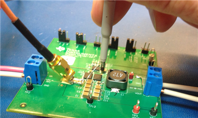 Figure 3 EVM Probing Technique
Figure 4 shows the switch-node and shunt waveforms at 300 kHz, 24 VIN, 5 VOUT and 4AOUT.
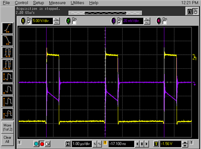 Figure 4 Silicon Bridge-Switching Waveforms
In Figure 4, yellow is the software node and purple is the top FET drain current. The average of the current “triangle” waveform matches well with the 4A load -> 20 mV = 4A.
In Figure 5, the highlighted reverse-recovery charge for the TPS40170/silicon MOSFET is shown in red (using the CSD185363A). The peak recovery current is ~ 18A (90 mV) and I estimate Qrr ~ <100 nC for a loss of 24V*300KHz*100nC = <720mW. Note that some of the current in the “red zone” goes to the load after the switch node rises, so my estimate may be a little high for Qrr.
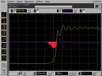 Figure 5 Silicon Bridge Reverse Recovery
Think about that! An 18A, 12 ns-wide current pulse is being drawn from the input supply every 3.33 µs. The high –di/dt will cause voltages to develop in any loop inductance in the power stage and possibly cause operational problems. Fortunately, the TPS40170EVM-597 has a very good layout to mitigate problems – it’s not always that way in practice.
Enter GaN – Where Is the Recovery?
I used the same technique to measure the LMG5200 GaN (Gallium Nitride) EVM. I first grabbed a reference scope shot of the switch-node voltage of the LMG5200EVM while it drove 24 V -> 5 V at a 4A load. I used an Agilent 33220A to drive a fixed ~21% duty cycle at 300 kHz to the LMG5200 PWM input. Channel 1 shows the switch-node waveform, see Figure 6.
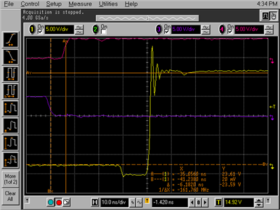 Figure 6 LMG5200 GaN Switching Waveforms
I included the high/low drive signals for reference (Channels 3 and 4). The “body diode” conduction has a higher drop than the MOSFET counterpart – I see approximately 2.5 V during this time instead of approximately 0.6 V. I grabbed this scope shot because I’m going to add a resistor/inductance to the input loop that will cause a bit more ringing.
Figure 7 shows the change when I added the shunt resistor in the drain of the upper GaN device.
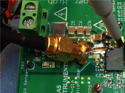 Figure 7 GaN Switching-Waveform Probe Technique
Note that I had to implement a level-shift circuit (simple PNP and resistor) to level shift the 300 kHz 21% duty-function generator signal from “ground” (which is now the positive side of the 24 V supply) to the PWM input at -24 V. Without that, I’d have a ground contention (otherwise known as a blown fuse) when putting the scope sensing on the positive rail. Figure 8 shows the switch node (yellow) and top GaN current (purple).
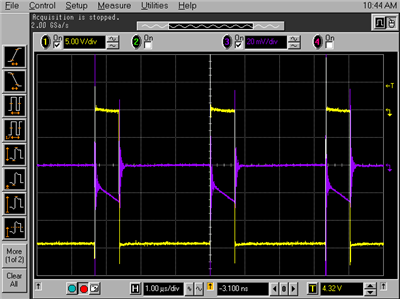 Figure 8 LMG5200 GaN Switching Waveforms With Shunt Inserted
Zooming in on Figure 9, the recovery current has disappeared (no red area). There is a little additional ringing due to the added inductance from the sense resistor, but no recovery losses or associated complications. You’ll still see switching and switch-node capacitance losses, but GaN does not show the reverse recovery that causes issues in silicon MOSFET-based converters – a welcome relief!
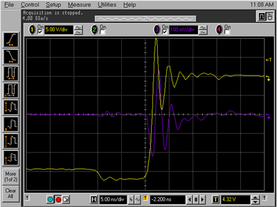 Figure 9 GaN Qrr Measurements
IMPORTANT NOTICE AND DISCLAIMER
TI PROVIDES TECHNICAL AND RELIABILITY DATA (INCLUDING DATASHEETS), DESIGN RESOURCES (INCLUDING REFERENCE DESIGNS), APPLICATION OR OTHER DESIGN ADVICE, WEB TOOLS, SAFETY INFORMATION, AND OTHER RESOURCES “AS IS” AND WITH ALL FAULTS, AND DISCLAIMS ALL WARRANTIES, EXPRESS AND IMPLIED, INCLUDING WITHOUT LIMITATION ANY IMPLIED WARRANTIES OF MERCHANTABILITY, FITNESS FOR A PARTICULAR PURPOSE OR NON-INFRINGEMENT OF THIRD PARTY INTELLECTUAL PROPERTY RIGHTS.
These resources are intended for skilled developers designing with TI products. You are solely responsible for (1) selecting the appropriate TI products for your application, (2) designing, validating and testing your application, and (3) ensuring your application meets applicable standards, and any other safety, security, or other requirements. These resources are subject to change without notice. TI grants you permission to use these resources only for development of an application that uses the TI products described in the resource. Other reproduction and display of these resources is prohibited. No license is granted to any other TI intellectual property right or to any third party intellectual property right. TI disclaims responsibility for, and you will fully indemnify TI and its representatives against, any claims, damages, costs, losses, and liabilities arising out of your use of these resources.
TI’s products are provided subject to TI’s Terms of Sale (www.ti.com/legal/termsofsale.html) or other applicable terms available either on ti.com or provided in conjunction with such TI products. TI’s provision of these resources does not expand or otherwise alter TI’s applicable warranties or warranty disclaimers for TI products.
Mailing Address: Texas Instruments, Post Office Box 655303, Dallas, Texas 75265
Copyright © 2023, Texas Instruments Incorporated