Voltage and Current Sensing in HEV/EV Applications
This post was co-authored by Ryan Small .
The rapid increase of semiconductor content in automotive systems has prompted a need to manage key voltages and currents in each subsystem. Supervising supply voltages, load currents or other important system functions can help indicate fault conditions, prevent catastrophic failures and protect end users from potential harm.
Hybrid electric vehicles (HEVs) and electric vehicles (EVs) have some distinct challenges compared to conventional combustion-powered vehicles. HEV and EV vehicles feature numerous systems that require monitoring voltages and currents, including the on-board charger (OBC), battery-management system (BMS), DC/DC converters and inverters. In this post, we’ll discuss the three fundamental circuits for monitoring current and voltage in HEV/EV systems: low-side current sensing with a difference amplifier (DA), in-line isolated current sensing and high-voltage sensing using an attenuating DA.
Figure 1 is a simplified HEV/EV block diagram showing common systems that require voltage and current monitoring.
 Figure 1 Typical HEV/EV System
While we won’t cover the operation of the subsystems in this post, designers sometimes use discrete DAs for low-side current sensing (as shown in Figure 2), particularly when the load current is bidirectional or they need a small reference voltage to pedestal the output to a known value greater than the amplifier’s minimum output swing. For the printed circuit board (PCB) layout, you should Kelvin-connect the shunt resistor. It is important to use a device with a common-mode voltage range that includes ground, such as the LM2904-Q1 or TLV313-Q1.
 Figure 2 Difference Amplifier for
Low-side Current Sensing
Figure 2 Difference Amplifier for
Low-side Current SensingEquation 1 gives the transfer function for this circuit, assuming R4 = R2 and R3 = R1. The amplifier for this application usually has a common-mode range that includes ground. Depending on the situation, however, the common-mode voltage may not be near ground because it actually depends on the voltage divider created by voltage across the shunt resistor (ILoad*Rsh), Vref and the ratio of R3 to R4. Make sure that the gain (R2/R1) is such that the output-voltage swing does not saturate.
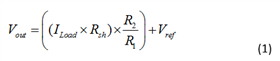
Figure 3 depicts a high-side, in-line isolated current-sensing solution. The AMC1200 is a differential-in, differential-out isolated amplifier. Isolated amplifiers help protect low-voltage circuitry from high common-mode voltages. The DA converts the differential signal to single-ended, which an analog-to-digital converter (ADC) can then digitize.
 Figure 3 Difference Amplifier Used for
Differential to Single-ended Conversion, Isolated In-line Sensing
Figure 3 Difference Amplifier Used for
Differential to Single-ended Conversion, Isolated In-line SensingEquation 2 gives the transfer function for the circuit shown in Figure 3, assuming R4 = R2 and R3 = R1. The gain of the AMC1200 is 8V/V. Vref typically connects to V2/2 to bias the output to mid supply to support bidirectional current. A rail-to-rail input/output (RRIO) amplifier such as the TLV313-Q1 is a good fit for this application.
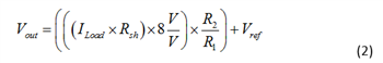 Figure 4 and Figure 5 depict an attenuating DA and the corresponding TINA-TI™ simulation.
In this circuit, the DA resistors divide the input voltage (±100V) down. Since the input
voltage is bipolar, a reference voltage set to mid supply biases the output. When
selecting the amplifier, be sure to comply with the device’s input common-mode and
output-voltage swing specifications. This example utilizes the OPA314-Q1 because
of its wide common-mode range.
Figure 4 and Figure 5 depict an attenuating DA and the corresponding TINA-TI™ simulation.
In this circuit, the DA resistors divide the input voltage (±100V) down. Since the input
voltage is bipolar, a reference voltage set to mid supply biases the output. When
selecting the amplifier, be sure to comply with the device’s input common-mode and
output-voltage swing specifications. This example utilizes the OPA314-Q1 because
of its wide common-mode range. Figure 4 Attenuating Difference
Amplifier
Figure 4 Attenuating Difference
Amplifier Figure 5 TINA-TI Software Simulation of
Attenuating Difference Amplifier
Figure 5 TINA-TI Software Simulation of
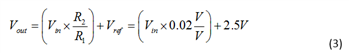
Attenuating Difference AmplifierEquation 3 gives the transfer function for the circuit shown in Figure 4, assuming R4 = R2 and R3 = R1. Notice that the gain is less than unity.
In this blog post, I presented three common circuits that appear in automotive subsystems such as the OBC, BMS, DC/DC converters and inverters. Additionally, I highlighted that HEV/EV applications use voltage and current sensing to monitor critical system functions, helping to maximize vehicle lifetimes. To learn more about the key operational amplifier specifications mentioned in this blog (for example, common-mode voltage) check out TI Precision Labs.
Additional Resources
- For additional information on PCB layout, read these blog posts:
- “The basics: How to layout a PCB for an op amp.”
- “How to layout a PCB for an instrumentation amplifier.”
- Watch the video, “TI Precision Labs – Op Amps: Input and Output Limitations.”
- Find common analog design formulas in the “Analog Engineer’s Pocket Reference.”
IMPORTANT NOTICE AND DISCLAIMER
TI PROVIDES TECHNICAL AND RELIABILITY DATA (INCLUDING DATASHEETS), DESIGN RESOURCES (INCLUDING REFERENCE DESIGNS), APPLICATION OR OTHER DESIGN ADVICE, WEB TOOLS, SAFETY INFORMATION, AND OTHER RESOURCES “AS IS” AND WITH ALL FAULTS, AND DISCLAIMS ALL WARRANTIES, EXPRESS AND IMPLIED, INCLUDING WITHOUT LIMITATION ANY IMPLIED WARRANTIES OF MERCHANTABILITY, FITNESS FOR A PARTICULAR PURPOSE OR NON-INFRINGEMENT OF THIRD PARTY INTELLECTUAL PROPERTY RIGHTS.
These resources are intended for skilled developers designing with TI products. You are solely responsible for (1) selecting the appropriate TI products for your application, (2) designing, validating and testing your application, and (3) ensuring your application meets applicable standards, and any other safety, security, or other requirements. These resources are subject to change without notice. TI grants you permission to use these resources only for development of an application that uses the TI products described in the resource. Other reproduction and display of these resources is prohibited. No license is granted to any other TI intellectual property right or to any third party intellectual property right. TI disclaims responsibility for, and you will fully indemnify TI and its representatives against, any claims, damages, costs, losses, and liabilities arising out of your use of these resources.
TI’s products are provided subject to TI’s Terms of Sale (www.ti.com/legal/termsofsale.html) or other applicable terms available either on ti.com or provided in conjunction with such TI products. TI’s provision of these resources does not expand or otherwise alter TI’s applicable warranties or warranty disclaimers for TI products.
Mailing Address: Texas Instruments, Post Office Box 655303, Dallas, Texas 75265
Copyright © 2023, Texas Instruments Incorporated