-
CDCM7005-SP 3.3-V High Performance Rad-Tolerant Class V, Clock Synchronizer and Jitter Cleaner
- 1 Features
- 2 Applications
- 3 Description
- 4 Revision History
- 5 Description (continued)
- 6 Pin Configuration and Functions
- 7 Specifications
- 8 Parameter Measurement Information
-
9 Detailed Description
- 9.1 Overview
- 9.2 Functional Block Diagram
- 9.3 Feature Description
- 9.4 Device Functional Modes
- 9.5 Programming
- 10Application and Implementation
- 11Power Supply Recommendations
- 12Layout
- 13Device and Documentation Support
- 14Mechanical, Packaging, and Orderable Information
- IMPORTANT NOTICE
CDCM7005-SP 3.3-V High Performance Rad-Tolerant Class V, Clock Synchronizer and Jitter Cleaner
1 Features
- High Performance LVPECL and LVCMOS PLL Clock Synchronizer
- Two Reference Clock Inputs (Primary and Secondary Clock) for Redundancy Support With Manual or Automatic Selection
- Accepts LVCMOS Input Frequencies Up to
200 MHz - VCXO_IN Clock is Synchronized to One of the Two Reference Clocks
- VCXO_IN Frequencies Up to 2 GHz (LVPECL)
- Outputs can be a Combination of LVPECL and LVCMOS (Up to Five Differential LVPECL Outputs or Up to 10 LVCMOS Outputs)
- Output Frequency is Selectable by x1, /2, /3, /4, /6, /8, /16 on Each Output Individually
- Efficient Jitter Cleaning from Low PLL Loop Bandwidth
- Low Phase Noise PLL Core
- Programmable Phase Offset (PRI_REF and SEC_REF to Outputs)
- Wide Charge Pump Current Range From
200 μA to 3 mA - Analog and Digital PLL Lock Indication
- Provides VBB Bias Voltage Output for Single-Ended Input Signals (VCXO_IN)
- Frequency Hold Over Mode Improves Fail-Safe Operation
- Power-Up Control Forces LVPECL Outputs to Tri-State at VCC < 1.5 V
- SPI Controllable Device Setting
- 3.3-V Power Supply
- High-Performance 52 Pin Ceramic Quad Flat Pack (HFG)
- Rad-Tolerant : 50 kRad (Si) TID
- QML-V Qualified, SMD 5962-07230
- Military Temperature Range: –55°C to 125°C Tcase
- Engineering Evaluation (/EM) Samples are Available (1)
2 Applications
- Low-Jitter Clock Distribution
- SERDES Links
- Analog Data Converters
- Digital-to-Analog Converters
3 Description
The CDCM7005-SP is a high-performance, low phase noise and low skew clock synchronizer that synchronizes a VCXO (voltage controlled crystal oscillator) or VCO (voltage controlled oscillator) frequency to one of the two reference clocks. The programmable pre-divider M and the feedback-dividers N and P give a high flexibility to the frequency ratio of the reference clock to VC(X)O as VC(X)O_IN / PRI_REF = (N × P) / M or VC(X)O_IN / SEC_REF = (N × P) / M.
VC(X)O_IN clock operates up to 2 GHz. Through the selection of external VC(X)O and loop filter components, the PLL loop bandwidth and damping factor can be adjust to meet different system requirements.
Device Information(1)
| PART NUMBER | PACKAGE | BODY SIZE (NOM) |
|---|---|---|
| CDCM7005-SP | CFP (52) | 13.97 mm × 13.97 mm |
- For all available packages, see the orderable addendum at the end of the data sheet.
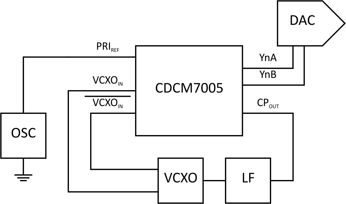
Typical Application Schematic
4 Revision History
Changes from F Revision (January 2014) to G Revision
- Added ESD Ratings table, Feature Description section, Device Functional Modes, Application and Implementation section, Power Supply Recommendations section, Layout section, Device and Documentation Support section, and Mechanical, Packaging, and Orderable Information section Go
- Deleted two bullets from the Features List. Go
Changes from E Revision (August 2012) to F Revision
Changes from D Revision (December 2011) to E Revision
- Changed PLL_LOCK pin description, replaced cycle-slip text.Go
- Changed the Frequency Hold-Over Mode sectionGo
- Changed text From: Cycle-Slip To: Frequency Offset in Figure 22Go
- Changed table Word 3, Cycle Slip (Bit 6) To: Frequency OffsetGo
- Changed Note 1 of table Word 3Go
- Changed table Lock-Detect Window (Word 3) - Clip slip To: Frequency offset, and Note 2Go
Changes from B Revision (December 2009) to C Revision
- Changed the VCC pin text - From: There is no internal connection between VCC and AVCC To: VCC and AVCC should always have same supply voltageGo
- Added to the CTRL_LE - Unused or floating inputs must be tied to proper logic level. It is recommended to use a 20-kΩ or larger pullup resistor to VCCGo
- Added to the CTRL_CLK pin - Unused or floating inputs must be tied to proper logic level. It is recommended to use a 20-kΩ or larger pullup resistor to VCCGo
- Added to the CTRL_DATA pin - Unused or floating inputs must be tied to proper logic level. It is recommended to use a 20-kΩ or larger pullup resistor to VCCGo
- Added to the PD pin text - It is recommended to ramp up the...Go
- Added to the SPI CONTROL INTERFACE section - Unused or floating inputs must be tied to proper logic level. It is recommended to use a 20-kΩ or larger pullup resistor to VCCGo
- Added to the SPI CONTROL INTERFACE section - It is recommended to program Word 0, Word 1, Word 2 and Word 3 right after power up and PD becomes HIGHGo
- Changed bit 16 from RES to GTMEGo
- Changed bit 28 from RES to PFDFCGo
5 Description (continued)
The CDCM7005-SP can lock to one of two reference clock inputs (PRI_REF and SEC_REF), supports frequency hold-over mode and fast-frequency-locking for fail-safe and increased system redundancy. The outputs of the CDCM7005-SP are user definable and can be any combination of up to five LVPECL outputs or up to 10 LVCMOS outputs. The LVCMOS outputs are arranged in pairs (Y0A:Y0B, Y1A:Y1B, …), so that each pair has the same frequency. But each output can be separately inverted and disabled. The built in synchronization latches ensure that all outputs are synchronized for low output skew.
All device settings, like outputs signaling, divider value, input selection, and many more, are programmable by SPI (3-wire serial peripheral interface). SPI allows individually control of the device settings.
The device operates in a 3.3-V environment and is characterized for operation from –55°C to 125°C (Tcase).
6 Pin Configuration and Functions
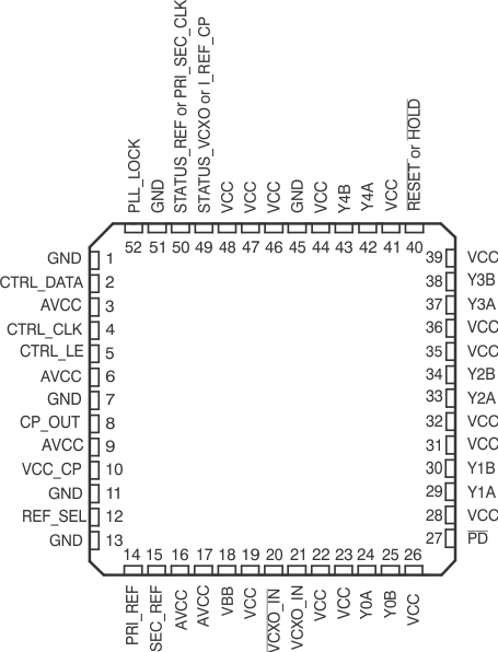
Pin Functions
7 Specifications
7.1 Absolute Maximum Ratings
over operating free-air temperature range (unless otherwise noted)(1)| MIN | MAX | UNIT | ||
|---|---|---|---|---|
| VCC, AVCC, VCC_CP |
Supply voltage (2) | –0.5 | 4.6 | V |
| VI | Input voltage (3) | –0.5 V | VCC + 0.5 V | V |
| VO | Output voltage (3) | –0.5 | VCC + 0.5 V | V |
| IOUT | Output current for LVPECL/LVCMOS outputs (0 < VO < VCC) |
±50 | mA | |
| IIN | Input current (VI < 0, VI > VCC) | ±20 | mA | |
| TJ | Maximum junction temperature | 150 | °C | |
| Tstg | Storage temperature | –65 | 150 | °C |
7.2 ESD Ratings
| VALUE | UNIT | |||
|---|---|---|---|---|
| V(ESD) | Electrostatic discharge | Human body model (HBM), per ANSI/ESDA/JEDEC JS-001(1) | ±2500 | V |
| Charged-device model (CDM), per JEDEC specification JESD22-C101(2) | ±1500 | |||
7.3 Recommended Operating Conditions
| MIN | NOM | MAX | UNIT | ||
|---|---|---|---|---|---|
| VCC, AVCC | Supply voltage | 3 | 3.3 | 3.6 | V |
| VCC_CP | 2.3 | VCC | |||
| VIL | Low-level input voltage LVCMOS, see (2) | 0.3 VCC | V | ||
| VIH | High-level input voltage LVCMOS, see (2) | 0.7 VCC | V | ||
| IOH | High-level output current LVCMOS (includes all status pins) | –8 | mA | ||
| IOL | Low-level output current LVCMOS (includes all status pins) | 8 | mA | ||
| VI | Input voltage range LVCMOS | 0 | 3.6 | V | |
| VINPP | Input amplitude LVPECL (VVCXO_IN – V VCXO_IN )(1) | 0.5 | 1.3 | V | |
| VIC | Common-mode input voltage LVPECL | 1 | VCC–0.3 | V | |
| TC | Operating case temperature | –55 | 125 | °C | |
of 150 mV.
7.4 Thermal Information
| THERMAL METRIC(1) | CDCM7005-SP(2) | UNIT | |
|---|---|---|---|
| HFG (CFP) | |||
| 52 PINS | |||
| RθJA | Junction-to-free-air thermal resistance(3) | 21.813 | °C/W |
| RθJC | Junction-to-case thermal resistance(4) | 0.849 | °C/W |
7.5 Electrical Characteristics
over recommended operating free-air temperature range (unless otherwise noted)| PARAMETER | TEST CONDITIONS | MIN | TYP(1) | MAX | UNIT | |
|---|---|---|---|---|---|---|
| OVERALL | ||||||
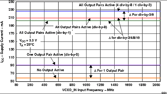
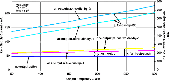
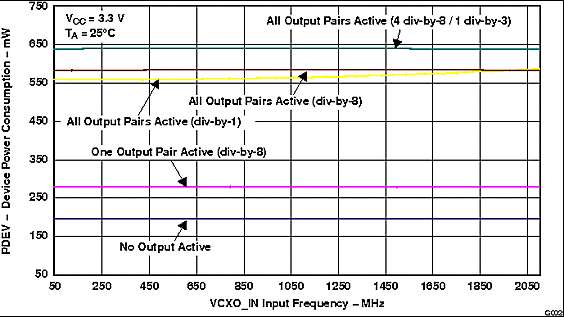
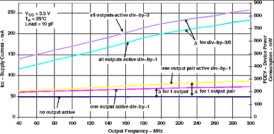
| ICC_LVPECL | Supply current (ICC over frequency see Figure 2 through Figure 5) | ƒVCXO = 200 MHz, ƒREF_IN = 25 MHz, PFD = 195.3125 kHz, ICP = 2 mA, all outputs are LVPECL and Div-by-8 (load, see Figure 14) |
210 | 260 | mA | |
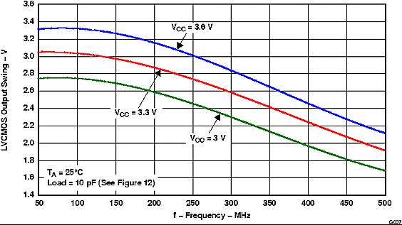
| ICC_LVCMOS | ƒVCXO = 200 MHz, ƒREF_IN = 25 MHz, PFD = 195.3125 kHz, ICP = 2 mA, All outputs are LVCMOS and Div-by-8 (load, 10 pF) |
120 | 160 | mA | ||
| ICCPD | Power-down current | ƒIN = 0 MHz, VCC = 3.6 V, AVCC = 3.6 V, VCC_CP = 3.6 V, VI = 0 V or VCC |
100 | 300 | µA | |
| IOZ | High-impedance state output current for Yx outputs | VO = 0 V or VCC – 0.8 V | ±40 | µA | ||
| VO = 0 V or VCC | ±100 | µA | ||||
| VI_REF_CP | Voltage on I_REF_CP (external current path for accurate charge pump current) | 12 kΩ to GND at pin 49 | 1.114 | 1.21 | 1.326 | V |
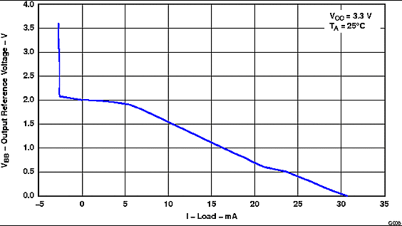
| VBB | Output reference voltage | VCC = 3 V – 3.6 V; IBB = –0.2 mA | VCC–1.446 | VCC–1.3 | VCC–1.09 | V |
| CO | Output capacitance for Yx | VCC = 3.3 V, VO = 0 V or VCC | 3 | pF | ||
| CI | Input capacitance at PRI_REF and SEC_REF | VI = 0 V or VCC, VI = 0 V or VCC | 3.6 | pF | ||
| Input capacitance at CTRL_LE, CTRL_CLOCK, CTRL_DATA | VI = 0 V or VCC | 3 | ||||
| LVCMOS | ||||||
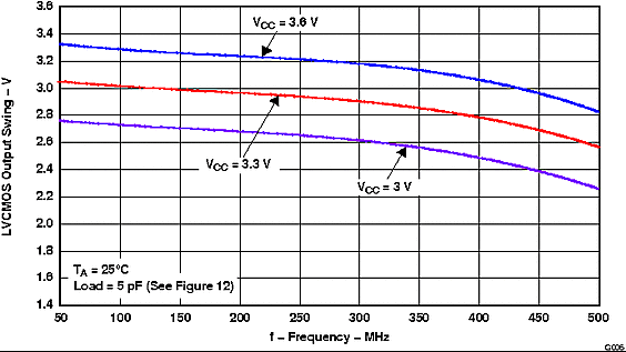
| ƒclk | Output frequency (see (2), (3), Figure 7, and Figure 8) | Load = 5 pF to GND, 1 kΩ to VCC, 1 kΩ to GND | 240 | MHz | ||
| VIK | LVCMOS input clamp voltage | VCC = 3 V, II = –18 mA | –1.2 | V | ||
| II | LVCMOS input current for CTRL_LE, CTRL_CLK, CTRL_DATA | VI = 0 V or VCC, VCC = 3.6 V | ±5 | µA | ||
| IIH | LVCMOS input current for PD, RESET, HOLD, REF_SEL, PRI_REF, SEC_REF, (see (4)) | VI = VCC, VCC = 3.6 V | 5 | µA | ||
| IIL | LVCMOS input current for PD, RESET, HOLD, REF_SEL, PRI_REF, SEC_REF (see (4)) | VI = 0 V, VCC = 3.6 V | –15 | –35 | µA | |
| VOH | High-level output voltage for LVCMOS outputs | VCC = min to max, IOH = –100 μA |
VCC–0.1 | V | ||
| VCC = 3 V, IOH = –6 mA | 2.4 | |||||
| VCC = 3 V, IOH = –12 mA | 2 | |||||
| VOL | Low-level output voltage for LVCMOS outputs | VCC = min to max, IOL = 100 μA |
0.1 | V | ||
| VCC = 3 V, IOL = 6 mA | 0.5 | |||||
| VCC = 3 V, IOL = 12 mA | 0.8 | |||||
| IOH | High-level output current | VCC = 3.3 V, VO = 1.65 V | –50 | –30 | –20 | mA |
| IOL | Low-level output current | VCC = 3.3 V, VO = 1.65 V | 20 | 30 | 50 | mA |
| tpho | Phase offset (REF_IN to Y output)(6) | VREF_IN = VCC/2, Y = VCC/2, see Figure 12, Load = 10 pF |
2.7 | ns | ||
| tsk(p) | LVCMOS pulse skew, see Figure 11 | Crosspoint to VCC/2 load, see Figure 13 | 160 | ps | ||
| tpd(LH) | Propagation delay from VCXO_IN to Yx, see Figure 11 | Crosspoint to VCC/2, Load = 10 pF, see Figure 13 (PLL bypass mode) |
2.8 | ns | ||
| tpd(HL) | ||||||
| tsk(o) | LVCMOS single-ended output skew, see (7) and Figure 11 | All outputs have the same divider ratio | 80 | ps | ||
| Outputs have different divider ratios | 80 | |||||
| Duty cycle | LVCMOS | VCC/2 to VCC/2 | 49% | 51% | ||
| tslew-rate | Output rise/fall slew rate | 20% to 80% of swing (load see Figure 13) |
3.5 | V/ns | ||
| LVPECL | ||||||
| ƒclk | Output frequency, see (3) and Figure 6 | Load, see Figure 14 | 0 | 2000 | MHz | |
| II | LVPECL input current | VI = 0 V or VCC | ±20 | µA | ||
| VOH | LVPECL high-level output voltage | Load, See Figure 14 | VCC–1.18 | VCC–0.81 | V | |
| VOL | LVPECL low-level output voltage | Load, See Figure 14 | VCC–2 | VCC–1.55 | V | |
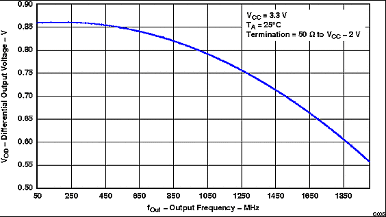
| |VOD| | Differential output voltage | See Figure 10 and load, see Figure 14 | 500 | mV | ||
| tpho | Phase offset (REF_IN to Y output)(7) | VREF_IN = VCC/2 to cross point of Y, see Figure 12 | 250 | ps | ||
| tpd(LH) | Propagation delay time, VCXO_IN to Yx, see Figure 11 | Cross point-to-cross point, load see Figure 14 |
615 | ps | ||
| tpd(HL) | ||||||
| tsk(p) | LVPECL pulse skew, see Figure 11 | Cross point-to-cross point, load see Figure 14 |
15 | ps | ||
| tsk(o) | LVPECL output skew(7) | Load see Figure 14, all outputs have the same divider ratio | 20 | ps | ||
| Load see Figure 14, outputs have different divider ratios |
50 | |||||
| tr / tf | Rise and fall time | 20% to 80% of VOUTPP, see Figure 10 | 170 | ps | ||
| CI | Input capacitance at VCXO_IN, VCXO_IN | 2.5 | pF | |||
| LVCMOS-TO-LVPECL | ||||||
| tsk(P_C) | Output skew between LVCMOS and LVPECL outputs, see (8) and Figure 11 | Cross point to VCC/2; load, see Figure 13 and Figure 14 |
2 | 3.2 | ns | |
| PLL ANALOG LOCK | ||||||
| IOH | High-level output current | VCC = 3.6 V, VO = 1.8 V | –150 | –110 | –80 | µA |
| IOL | Low-level output current | VCC = 3.6 V, VO = 1.8 V | 80 | 110 | 150 | µA |
| IOZH LOCK | High-impedance state output current for PLL LOCK output(5) | VO = 3.6 V (PD is set low) | 45 | 65 | µA | |
| IOZL LOCK | High-impedance state output current for PLL LOCK output(5) | VO = 0 V (PD is set low) | ±5 | µA | ||
| VIT+ | Positive input threshold voltage | VCC = min to max | VCC×0.55 | V | ||
| VIT– | Negative input threshold voltage | VCC = min to max | VCC×0.35 | V | ||
| PHASE DETECTOR | ||||||
| ƒCPmax | Maximum charge pump frequency | Default PFD pulse width delay | 100 | MHz | ||
| CHARGE PUMP | ||||||
| ICP | Charge pump sink/source current range (9) | VCP = 0.5 VCC_CP | ±0.2 | ±3.9 | mA | |
| ICP3St | Charge pump 3-state current | Temperature = 25°C, 0.5 V < VCP < VCC_CP – 0.5 V | –10 | 10 | nA | |
| Temperature = –55°C to 125°C, 0.5 V < VCP < VCC_CP – 0.5 V | –50 | 50 | ||||
| ICPA | ICP absolute accuracy | VCP = 0.5 VCC_CP, internal reference resistor, SPI default settings | –20% | 10% | 20% | |
| VCP = 0.5 VCC_CP, external reference resistor 12 kΩ (1%) at I_REF_CP, SPI default settings | 5% | |||||
| ICPM | Sink/source current matching | 0.5 V < VCP < VCC_CP – 0.5 V, SPI default settings | –7% | 2.5% | 7% | |
| IVCPM | ICP vs VCP matching | 0.5 V < VCP < VCC_CP – 0.5 V | –10% | 5% | 10% | |
7.6 Timing Requirements
over recommended ranges of supply voltage, load and operating free air temperature| MIN | TYP | MAX | UNIT | ||
|---|---|---|---|---|---|
| PRI_REF/SEC_REF_IN REQUIREMENTS | |||||
| ƒREF_IN | LVCMOS primary or secondary reference clock frequency(1) (4) | 0 | 200 | MHz | |
| tr/ tf | Rise and fall time of PRI_REF or SEC_REF signals from 20% to 80% of VCC | 4 | ns | ||
| dutyREF | Duty cycle of PRI_REF or SEC_REF at VCC/2 | 40% | 60% | ||
| VCXO_IN, VCXO_IN REQUIREMENTS | |||||
| ƒVCXO_IN | VCXO clock frequency(2) | 0 | 2000 | MHz | |
| tr/ tf | Rise and fall time 20% to 80% of VINPP at 80 MHz to 800 MHz(3) | 3 | ns | ||
| dutyVCXO | Duty cycle of VCXO clock | 40% | 60% | ||
| SPI/CONTROL REQUIREMENTS (see Figure 24) | |||||
| ƒCTRL_CLK | CTRL_CLK frequency | 20 | MHz | ||
| tsu1 | CTRL_DATA to CTRL_CLK setup time | 10 | ns | ||
| th2 | CTRL_DATA to CTRL_CLK hold time | 10 | ns | ||
| t3 | CTRL_CLK high duration | 25 | ns | ||
| t4 | CTRL_CLK low duration | 25 | ns | ||
| tsu5 | CTRL_LE to CTRL_CLK setup time | 10 | ns | ||
| tsu6 | CTRL_CLK to CTRL_LE setup time | 10 | ns | ||
| t7 | CTRL_LE pulse width | 20 | ns | ||
| tr/ tf | Rise and fall time of CTRL_DATA CTRL_CLK, CTRL_LE from 20% to 80% of VCC | 4 | ns | ||
| PD, RESET, HOLD , REF_SEL REQUIREMENTS | |||||
| tr / tf | Rise and fall time of the PD, RESET, HOLD, REF_SEL signal from 20% to 80% of VCC | 4 | ns | ||
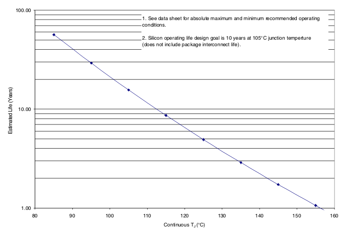 Figure 1. CDCM7005-SPHFG-V - 52-Pin HFG Package
Operating Life Derating Chart
7.7 Typical Characteristics
