Large Duty Cycle Operation On the TPS563211
Trademarks
All trademarks are the property of their respective owners.
1 TPS563211 Introduction
The TPS563211 is a cost effective and highly flexible synchronous buck converter that provides selectable Eco-mode operation or FCCM (Force Continuous Conduction Mode) operation. Selectable Power-Good indicator or external Soft-Start is also configurable through the MODE pin. Power sequencing is possible by correctly configuring the Enable, Power-Good indicator or external Soft-Start. A wide input voltage range of 4.2 V to 18 V supports a wide variety of common input rails like 12 V and 15 V. It supports up to 3 A continuous output current at output voltages between 0.6 V and 7 V.
The device provides fast transient response with true fixed switching frequency through the use of the Advanced Emulated Current Mode (AECM) control topology. With internal smart loop bandwidth control, the device provides fast transient response over a wide output voltage range without the need for external compensation.
2 TPS563211 Control Architecture
2.1 AECM Control on TPS563211
AECM is a new topology based on a fixed-frequency modulator with emulated current information for the loop control, combing the fixed frequency of PCM control and the fast load-transient response of the D-CAP2 control topology. The key features and benefits of AECM include:
- True fixed-frequency modulation that can simplify EMI filter design and make it easy to achieve high-frequency modulation such as 2.1 MHz.
- An emulated ramp-generator circuit with smart loop-bandwidth control that can adjust the DC gain smartly, supporting wide-output and large-duty-cycle applications with good load-transient performance.
Figure 2-1 shows the detailed control block diagram in the TPS563211 design.
 Figure 2-1 TPS563211 Functional Block
Diagram
Figure 2-1 TPS563211 Functional Block
DiagramTo improve noise immunity with virtually no ripple on the output voltage, an additional RAMP is added. An included error amplifier makes the output voltage very accurate.
In the control block of the TPS563211 device, the inductor valley current is monitored by measuring the SW node voltage during low-side MOSFET ON-time, which leads a minimum off time requirement for the high-side MOSFET. When the ON timer is expired, the high-side MOSFET is turned off and the low-side MOSFET is turned on. The turning off of the high-side MOSFET causes the SW ringing. When measuring the SW node voltage, a time delay needs to be included to let the internal SW node ringing dissipate. This time delay results in the minimum off time for the high-side MOSFET.
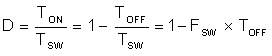
Based on Equation 1, since Toff has a minimum value, it follows that the duty cycle, D, has a maximum value. If the FSW is fixed, a smaller TOFF(min), means a larger duty cycle can be supported. Alternatively, if the TOFF(min) is fixed, a larger duty cycle can be supported with a smaller FSW.
In the TPS563211 device, the minimum off time of low-side MOSFET is 105 ns and the maximum on time is 6 μs which result in a maximum duty cycle of about 98% during normal operation.