SLPS388B September 2012 – January 2015 CSD18533Q5A
PRODUCTION DATA.
- 1Features
- 2Applications
- 3Description
- 4Revision History
- 5Specifications
- 6Device and Documentation Support
- 7Mechanical, Packaging, and Orderable Information
Package Options
Refer to the PDF data sheet for device specific package drawings
Mechanical Data (Package|Pins)
- DQJ|8
Thermal pad, mechanical data (Package|Pins)
Orderable Information
1 Features
2 Applications
- DC-DC Conversion
- Secondary Side Synchronous Rectifier
- Motor Control
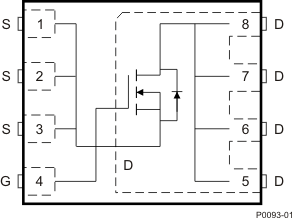
3 Description
This 4.7 mΩ, 60 V, SON 5 × 6 mm NexFET™ power MOSFET is designed to minimize losses in power conversion applications.
Top View
Product Summary
| TA = 25°C | TYPICAL VALUE | UNIT | ||
|---|---|---|---|---|
| VDS | Drain-to-Source Voltage | 60 | V | |
| Qg | Gate Charge Total (10 V) | 29 | nC | |
| Qgd | Gate Charge Gate-to-Drain | 5.4 | nC | |
| RDS(on) | Drain-to-Source On-Resistance | VGS = 4.5 V | 6.5 | mΩ |
| VGS = 10 V | 4.7 | mΩ | ||
| VGS(th) | Threshold Voltage | 1.9 | V | |
Ordering Information(1)
| Device | Qty | Media | Package | Ship |
|---|---|---|---|---|
| CSD18533Q5A | 2500 | 13-Inch Reel | SON 5 mm × 6 mm Plastic Package | Tape and Reel |
| CSD18533Q5AT | 250 | 7-Inch Reel |
- For all available packages, see the orderable addendum at the end of the data sheet.
Absolute Maximum Ratings
| TA = 25°C | VALUE | UNIT | |
|---|---|---|---|
| VDS | Drain-to-Source Voltage | 60 | V |
| VGS | Gate-to-Source Voltage | ±20 | V |
| ID | Continuous Drain Current (Package limited), TC = 25°C | 100 | A |
| Continuous Drain Current (Silicon limited), TC = 25°C | 103 | ||
| Continuous Drain Current, TA = 25°C(1) | 17 | ||
| IDM | Pulsed Drain Current, TA = 25°C(2) | 267 | A |
| PD | Power Dissipation(1) | 3.2 | W |
| Power Dissipation, TC = 25°C | 116 | ||
| TJ, Tstg |
Operating Junction and Storage Temperature Range |
–55 to 150 | °C |
| EAS | Avalanche Energy, single pulse ID = 53 A, L = 0.1 mH, RG = 25 Ω |
140 | mJ |
RDS(on) vs VGS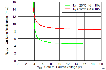 |
Gate Charge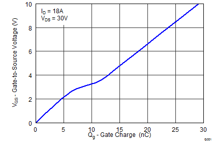 |