SNOSBJ2B August 2000 – January 2016 LM119
PRODUCTION DATA.
1 Features
- Two Independent Comparators
- Operates from a Single 5-V Supply
- Typically 80-ns Response Time at ±15 V
- Minimum Fan-out of 2 Each Side
- Maximum Input Current of 1 μA Over Temperature
- Inputs and Outputs can be Isolated from System Ground
- High Common-Mode Slew Rate
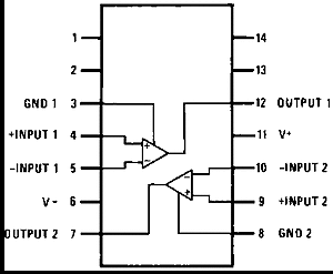
Connection Diagram
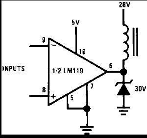
Typical Application - Relay Driver
2 Description
The LM119 series are precision high-speed dual comparators fabricated on a single monolithic chip. They are designed to operate over a wide range of supply voltages down to a single 5-V logic supply and ground. They have higher gain and lower input currents than devices such as the LM710. The uncommitted collector of the output stage makes the LM119 compatible with RTL, DTL, and TTL, as well as capable of driving lamps and relays at currents of up to 25 mA.
The LM319A offers improved precision over the standard LM319, with tighter tolerances on offset voltage, offset current, and voltage gain.
Although designed primarily for applications requiring operation from digital logic supplies, the LM119 series are fully specified for power supplies up to ±15 V. The series features faster response than the LM111, at the expense of higher power dissipation. However, the high-speed, wide operating voltage range and low package count make the LM119 more versatile than older devices such as the LM711.
The LM119 is specified from −55°C to +125°C, the LM219 is specified from −25°C to +85°C, and the LM319A and LM319 are specified from 0°C to +70°C.
Device Information(1)
| PART NUMBER | PACKAGE | BODY SIZE (NOM) |
|---|---|---|
| LM119, LM219, LM319 | TO-100 (10) | 8.96 mm × 8.96 mm |
| CDIP (14) | 6.67 mm × 19.56 mm |
- For all available packages, see the orderable addendum at the end of the data sheet.
3 Revision History
Changes from A Revision (May 2004) to B Revision
4 Pin Configuration and Functions

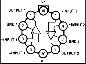
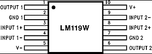
Pin Functions
| PIN | I/O | DESCRIPTION | |||
|---|---|---|---|---|---|
| NAME | NO. (D, J, NFF 14) |
NO. (LME 10) |
NO. (NAD 10) |
||
| OUTPUT 1 | 1 | 12 | 1 | O | Comparator 1 output |
| GND 1 | 2 | 3 | 2 | G | Comparator 1 ground connection |
| INPUT 1+ | 3 | 4 | 3 | I | Comparator 1 input |
| INPUT 1- | 4 | 5 | 4 | I | Comparator 1 input |
| V- | 5 | 6 | 5 | P | Negative supply voltage |
| OUTPUT 2 | 6 | 7 | 6 | O | Comparator 2 output |
| GND 2 | 7 | 8 | 7 | G | Comparator 2 ground connection |
| INPUT 2+ | 8 | 9 | 8 | I | Comparator 2 input |
| INPUT 2- | 9 | 10 | 9 | I | Comparator 2 input |
| V+ | 10 | 11 | 10 | P | Positive supply voltage |
| NC | 1,2,13,14 | No connect. Do not connect to ground. | |||