SNVS593J October 2008 – November 2014 LM25085 , LM25085-Q1
PRODUCTION DATA.
- 1 Features
- 2 Applications
- 3 Description
- 4 Revision History
- 5 Pin Configuration and Functions
- 6 Specifications
- 7 Detailed Description
- 8 Application and Implementation
- 9 Power Supply Recommendations
- 10Layout
- 11Device and Documentation Support
- 12Mechanical, Packaging, and Orderable Information
1 Features
- LM25085-Q1 is an Automotive Grade product that is AEC-Q100 Grade 1 Qualified (-40°C to 125°C Operating Junction Temperature)
- Wide 4.5V to 42V Input Voltage Range
- Adjustable Current Limit Using RDS(ON) or a Current Sense Resistor
- Programmable Switching Frequency to 1MHz
- No Loop Compensation Required
- Ultra-Fast Transient Response
- Nearly Constant Operating Frequency with Line and Load Variations
- Adjustable Output Voltage from 1.25V
- Precision ±2% Feedback Reference
- Capable of 100% Duty Cycle Operation
- Internal Soft-Start Timer
- Integrated High Voltage Bias Regulator
- Thermal Shutdown
2 Applications
- Automotive Infotainment
- Battery/Super Capacitor Chargers
- LED Drivers
3 Description
The LM25085 is a high efficiency PFET switching regulator controller that can be used to quickly and easily develop a small, efficient buck regulator for a wide range of applications. This high voltage controller contains a PFET gate driver and a high voltage bias regulator which operates over a wide 4.5V to 42V input range. The constant on-time regulation principle requires no loop compensation, simplifies circuit implementation, and results in ultra-fast load transient response. The operating frequency remains nearly constant with line and load variations due to the inverse relationship between the input voltage and the on-time. The PFET architecture allows 100% duty cycle operation for a low dropout voltage. Either the RDS(ON) of the PFET or an external sense resistor can be used to sense current for over-current detection.
Device Information(1)
| PART NUMBER | PACKAGE | BODY SIZE (NOM) |
|---|---|---|
| LM25085-Q1 | HVSSOP (8) | 3.00 mm x 3.00 mm |
| LM25085 | VSSOP (8) | 3.00 mm x 3.00 mm |
| WSON (8) | 3.00 mm x 3.00 mm | |
| HVSSOP (8) | 3.00 mm x 3.00 mm |
- For all available packages, see the orderable addendum at the end of the datasheet.
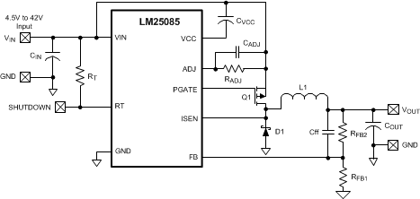
Simplified Schematic
