Data Sheet
UCC21732-Q1 适用于 SiC/IGBT 并具有主动保护、隔离式模拟检测和高 CMTI 的汽车类 10A 拉电流/灌电流增强型隔离式单通道栅极驱动器
本资源的原文使用英文撰写。 为方便起见,TI 提供了译文;由于翻译过程中可能使用了自动化工具,TI 不保证译文的准确性。 为确认准确性,请务必访问 ti.com 参考最新的英文版本(控制文档)。
1 特性
- 5.7kVRMS 单通道隔离式栅极驱动器
- 符合面向汽车应用的 AEC-Q100 标准
- 器件温度等级 1:–40°C 至 +125°C 环境工作温度范围
- 器件 HBM ESD 分类等级 3A
- 器件 CDM ESD 分类等级 C3
- 高达 2121Vpk 的 SiC MOSFET 和 IGBT
- 33V 最大输出驱动电压 (VDD-VEE)
- ±10A 驱动强度和分离输出
- 150V/ns 最小 CMTI
- 具有 270ns 快速响应时间的过流保护
- 外部有源米勒钳位
- 发生故障时的内部 2 级关断
- 具有 PWM 输出的隔离式模拟传感器
- 采用 NTC、PTC 或热敏二极管的温度感应
- 高电压直流链路或相电压
- 过流警报 FLT 和通过 RST/EN 重置
- 针对 RST/EN 的快速启用/禁用响应
- 抑制输入引脚上的 <40ns 噪声瞬态和脉冲
- RDY 上的 12V VDD UVLO(具有电源正常指示功能)
- 具有高达 5V 的过冲/欠冲瞬态电压抗扰度的输入/输出
- 130ns(最大)传播延迟和 30ns(最大)脉冲/器件间偏移
- SOIC-16 DW 封装,爬电距离和间隙 > 8mm
- 工作结温范围:-40°C 至 +150°C
- 安全相关认证:
- 符合 DIN EN IEC 60747-17 (VDE 0884-17) 要求的 8000VPK VIOTM 和 2121VPK VIORM 增强型隔离
- 5700VRMS 隔离,符合 UL1577 标准且持续时长为 1 分钟
2 应用
- 适用于 EV 的牵引逆变器
- 车载充电器和充电桩
- 用于 HEV/EV 的直流/直流转换器
3 说明
UCC21732-Q1 是一款电隔离单通道栅极驱动器,旨在用于 SiC MOSFET 和 IGBT,工作电压高达 2121V(直流),具有先进的保护特性、出色的动态性能和稳健性。UCC21732-Q1 具有高达 ±10A 的峰值拉电流和灌电流。
输入侧通过 SiO2 电容隔离技术与输出侧相隔离,支持高达 1.5kVRMS 的工作电压、12.8kVPK 的浪涌抗扰度,隔离栅寿命超过 40 年,并提供较低的器件间偏斜,共模噪声抗扰度 (CMTI) 大于 150V/ns。
UCC21732-Q1 包括先进的保护特性,如快速过流和短路检测、分流电流检测支持、故障报告、有源米勒钳位、输入和输出侧电源 UVLO(用于优化 SiC 和 IGBT 开关行为)和稳健性。可以利用隔离式模拟至 PWM 传感器更轻松地进行温度或电压感测,从而进一步提高驱动器的多功能性并简化系统设计工作量、尺寸和成本。
器件信息
| 器件型号 | 封装(1) | 封装尺寸(标称值) |
|---|---|---|
| UCC21732-Q1 | DW(SOIC,16) | 10.3mm × 7.5mm |
(1) 有关所有可选封装,请参阅 节 13。
器件引脚配置
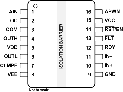
4 Pin Configuration and Functions
Top
View") Figure 4-1 UCC21732-Q1DW SOIC (16)Top
View
Figure 4-1 UCC21732-Q1DW SOIC (16)Top
ViewTable 4-1 Pin Functions
| PIN | I/O(1) | DESCRIPTION | |
|---|---|---|---|
| NAME | NO. | ||
| AIN | 1 | I | Isolated analog sensing input, parallel a small capacitor to COM for better noise immunity. Tie to COM if unused. |
| OC | 2 | I | Over current detection pin, support lower threshold for SenseFET, DESAT, and Shunt resistor sensing. Tie to COM if unused. |
| COM | 3 | P | Common ground reference, connecting to emitter pin for IGBT and source pin for SiC-MOSFET |
| OUTH | 4 | O | Gate driver output pull up |
| VDD | 5 | P | Positive supply rail for gate drive voltage, Bypassing a >10-μF capacitor to COM to support specified gate driver source peak current capability. Place decoupling capacitor close to the pin. |
| OUTL | 6 | O | Gate driver output pull down |
| CLMPE | 7 | O | External Active miller clamp, connecting this pin to the gate of the external miller clamp MOSFET. Leave floating if unused. |
| VEE | 8 | P | Negative supply rail for gate drive voltage. Bypassing a >10-μF capacitor to COM to support specified gate driver sink peak current capability. Place decoupling capacitor close to the pin. |
| GND | 9 | P | Input power supply and logic ground reference |
| IN+ | 10 | I | Non-inverting gate driver control input. Tie to VCC if unused. |
| IN– | 11 | I | Inverting gate driver control input. Tie to GND if unused. |
| RDY | 12 | O | Power good for VCC-GND and VDD-COM. RDY is open drain configuration and can be paralleled with other RDY signals |
| FLT | 13 | O | Active low fault alarm output upon overcurrent or short circuit. FLT is in open drain configuration and can be paralleled with other faults |
| RST/EN | 14 | I | The
RST/EN serves two purposes: 1) Enable / shutdown of the output side. The FET is turned off by a regular turn-off, if terminal EN is set to low; 2) Resets the OC condition signaled on FLT pin. if terminal RST/EN is set to low for more than 1000 ns. A reset of signal FLT is asserted at the rising edge of terminal RST/EN. For automatic RESET function, this pin only serves as an EN pin. Enable / shutdown of the output side. The FET is turned off by a general turn-off, if terminal EN is set to low. |
| VCC | 15 | P | Input power supply from 3 V to 5.5 V, bypassing a >1-μF capacitor to GND. Place decoupling capacitor close to the pin. |
| APWM | 16 | O | Isolated Analog Sensing PWM output. Leave floating if unused. |
(1) P = Power, G = Ground, I = Input, O = Output
5 Specifications
5.1 Absolute Maximum Ratings
over operating free-air temperature range (unless otherwise noted)(1)
| PARAMETER | MIN | MAX | UNIT | ||
|---|---|---|---|---|---|
| VCC | VCC – GND | –0.3 | 6 | V | |
| VDD | VDD – COM | –0.3 | 36 | V | |
| VEE | VEE – COM | –17.5 | 0.3 | V | |
| VMAX | VDD – VEE | –0.3 | 36 | V | |
| IN+, IN–, RST/EN | DC | GND–0.3 | VCC | V | |
| Transient, less than 100 ns(2) | GND–5.0 | VCC+5.0 | V | ||
| AIN | Reference to COM | –0.3 | 5 | V | |
| OC | Reference to COM | -0.3 | 6 | ||
| OUTH, OUTL | DC | VEE–0.3 | VDD | V | |
| Transient, less than 100 ns(2) | VEE–5.0 | VDD+5.0 | V | ||
| CLMPE | Reference to VEE | –0.3 | 5 | V | |
| RDY, FLT, APWM | GND–0.3 | VCC | V | ||
| IFLT, IRDY | FLT, and RDY pin input current | 20 | mA | ||
| IAPWM | APWM pin output current | 20 | mA | ||
| TJ | Junction temperature range | –40 | 150 | °C | |
| Tstg | Storage temperature range | –65 | 150 | °C | |
(1) Stresses beyond those listed under absolute maximum ratings may cause permanent damage to the device. These are stress ratings only and functional operation of the device at these or any other conditions beyond those indicated under recommended operating conditions is not implied. Exposure to absolute-maximum-rated conditions for extended periods may affect device reliability.
(2) Values are verified by characterization on bench.
5.2 ESD Ratings
| VALUE | UNIT | |||
|---|---|---|---|---|
| V(ESD) | Electrostatic discharge | Human-body model (HBM), per AEC Q100-002(1) | ±4000 | V |
| Charged-device model (CDM), per AEC Q100-011 | ±1500 | |||
(1) AEC Q100-002 indicates that HBM stressing shall be in accordance with the ANSI/ESDA/JEDEC JS-001 specification.
5.3 Recommended Operating Conditions
| PARAMETER | MIN | MAX | UNIT | ||
|---|---|---|---|---|---|
| VCC | VCC–GND | 3.0 | 5.5 | V | |
| VDD | VDD–COM | 13 | 33 | V | |
| VMAX | VDD–VEE | – | 33 | V | |
| IN+, IN–, RST/EN | Reference to GND | High level input voltage | 0.7×VCC | VCC | V |
| Low level input voltage | 0 | 0.3×VCC | |||
| AIN | Reference to COM | 0.6 | 4.5 | V | |
| tRST/EN | Minimum pulse width that reset the fault | 1000 | ns | ||
| TA | Ambient Temperature | –40 | 125 | °C | |
| TJ | Junction temperature | –40 | 150 | °C | |
