-
LM27761 低噪声稳压开关电容器电压逆变器
- 1 特性
- 2 应用
- 3 说明
- 4 修订历史记录
- 5 Pin Configuration and Functions
- 6 Specifications
- 7 Detailed Description
-
8 Application and Implementation
- 8.1 Application Information
- 8.2
Typical Application - Regulated Voltage Inverter
- 8.2.1 Design Requirements
- 8.2.2 Detailed Design Procedure
- 8.2.3 Application Curves
- 9 Power Supply Recommendations
- 10Layout
- 11器件和文档支持
- 12机械、封装和可订购信息
- 重要声明
LM27761 低噪声稳压开关电容器电压逆变器
1 特性
- 对输入电源电压进行反相和稳压
- 低输出波纹
- 关断时可使静态电流降至 7µA(典型值)
- 输出电流高达 250mA
- 2.5Ω 逆变器输出阻抗,VIN = 5V
- 峰值负载时的稳定度为 ±4%
- 370µA 静态电流
- 2MHz(典型值)固定频率、低噪声运行
- 2MHz 频率时的低压降稳压器 (LDO) 电源抑制比 (PSRR) 为 35dB(典型值),
负载电流为 80mA - 100mA 电流时的 LDO 压降电压为 30mV,
VOUT = –5V - 限流和热保护
- 使用 LM27761 并借助 WEBENCH® 电源设计器创建定制设计
2 应用
- 运算放大器电源
- 无线通信系统
- 手机功率放大器偏置
- 接口电源
- 手持式仪表
- 高保真 (Hi-Fi) 耳机放大器
- 为数据转换器供电
3 说明
LM27761 低噪声稳压开关电容器电压逆变器可针对 2.7V 到 5.5V 范围内的输入电压,提供可调节的超低噪声输出。在应用解决方案中使用四个低成本电容器,可以提供高达 250mA 的输出电流。该器件的稳压输出可在 −5V 到 −1.5V 范围内进行调节。LM27761 以 2MHz(典型值)开关频率运行,以减小输出电阻和电压波纹。LM27761 的工作电流仅为 370µA(对于大多数负载,电荷泵功率效率均高于 80%)并且关断电流典型值为 7µA,因此在驱动功率放大器、DAC 偏置电源轨以及其他大电流、低噪声电压应用时, 可提供理想的性能。
器件信息(1)
| 器件型号 | 封装 | 封装尺寸(标称值) |
|---|---|---|
| LM27761 | WSON (8) | 2.00mm x 2.00mm |
典型应用
4 修订历史记录
Changes from B Revision (February 2016) to C Revision
- Added WEBENCH 链接Go
Changes from A Revision (December 2015) to B Revision
- Changed 典型应用图中位置颠倒的“C1”和“C2” Go
- Deleted footnote 3 to Abs Max table Go
- updated Specifications tablesGo
- Added Condition statement for Typical CharcteristicsGo
- Changed Figures 3 and 4; added Figures 16 through 18 Go
- Changed "... reducing the quiescent current to 1 µA" to "...reducing the quiescent current to 7 µA"Go
- Changed "1-µA typical shutdown current" to "7-µA typical shutdown current"Go
- Changed "C2 is charging C3" to "C1 is charging C3"Go
- Changed "VOUT" to "CPOUT" on Figure 20Go
- Changed "C2" to "C1" Go
- Changed "RSW" to "(2 × RSW)"Go
- Changed equation 1 Go
- Changed "–1.2 V" to "–1.22 V" Go
Changes from * Revision (October 2015) to A Revision
- Changed 器件文档形式,从单页产品预览改为完整的超前信息数据表Go
5 Pin Configuration and Functions
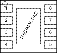
Pin Functions
| PIN | TYPE(1) | DESCRIPTION | |
|---|---|---|---|
| NUMBER | NAME | ||
| 1 | VIN | P | Positive power supply input. |
| 2 | GND | G | Ground |
| 3 | CPOUT | P | Negative unregulated output voltage. |
| 4 | VOUT | P | Regulated negative output voltage. |
| 5 | VFB | P | Feedback input. Connect VFB to an external resistor divider between VOUT and GND. DO NOT leave unconnected. |
| 6 | EN | I | Active high enable input. |
| 7 | C1– | P | Negative terminal for C1. |
| 8 | C1+ | P | Positive terminal for C1. |
| — | Thermal Pad | G | Ground. DO NOT leave unconnected. |
6 Specifications
6.1 Absolute Maximum Ratings
over operating free-air temperature range (unless otherwise noted)(1)(2)| MIN | MAX | UNIT | ||
|---|---|---|---|---|
| Ground voltage, VIN to GND or GND to VOUT | 5.8 | V | ||
| EN | (GND − 0.3 V) | (VIN + 0.3 V) | ||
| Continuous output current, CPOUT and VOUT | 300 | mA | ||
| TJMAX(3) | 150 | °C | ||
| Storage temperature, Tstg | –65 | 150 | °C | |
6.2 ESD Ratings
| VALUE | UNIT | |||
|---|---|---|---|---|
| V(ESD) | Electrostatic discharge | Human-body model (HBM), per ANSI/ESDA/JEDEC JS-001(1) | ±1000 | V |
| Charged-device model (CDM), per JEDEC specification JESD22-C101(2) | ±250 | |||
6.3 Recommended Operating Conditions
over operating free-air temperature range (unless otherwise noted)| MIN | MAX | UNIT | ||
|---|---|---|---|---|
| Operating ambient temperature, TA | –40 | 85 | °C | |
| Operating junction temperature, TJ | –40 | 125 | °C | |
| Operating input voltage, VIN | 2.7 | 5.5 | V | |
| Operating output current, IOUT | 0 | 250 | mA | |
6.4 Thermal Information
| THERMAL METRIC(1) | LM27761 | UNIT | |
|---|---|---|---|
| WSON (DSG) | |||
| 8 PINS | |||
| RθJA | Junction-to-ambient thermal resistance | 67.7 | °C/W |
| RθJC(top) | Junction-to-case (top) thermal resistance | 89.9 | °C/W |
| RθJB | Junction-to-board thermal resistance | 37.6 | °C/W |
| ψJT | Junction-to-top characterization parameter | 2.4 | °C/W |
| ψJB | Junction-to-board characterization parameter | 38 | °C/W |
| RθJC(bot) | Junction-to-case (bottom) thermal resistance | 9.4 | °C/W |
6.5 Electrical Characteristics
Typical limits apply for TA = 25°C, and minimum and maximum limits apply over the full temperature range. Unless otherwise specified, VIN = 5 V and values for C1 to C4 are as shown in the 典型应用.| PARAMETER | TEST CONDITIONS | MIN | TYP | MAX | UNIT | |
|---|---|---|---|---|---|---|
| Iq | Supply current | Open circuit, no load | 370 | 600 | µA | |
| ISD | Shutdown supply current | 7 | 12 | µA | ||
| ƒSW | Switching frequency | VIN = 3.6 V | 1.7 | 2 | 2.3 | MHz |
| RNEG | Output resistance to CPOUT | VIN = 5.5 V | 2 | Ω | ||
| VDO | LDO dropout voltage | ILOAD = 100 mA, VOUT = −5 V | 30 | mV | ||
| PSRR | Power supply rejection ratio | ILOAD = 80 mA, VCPOUT = −5 V | 35 | dB | ||
| VN | Output noise voltage | ILOAD = 80 mA, 10 Hz to 100 kHz | 20 | µVRMS | ||
| VFB | Feedback pin reference voltage | 1.202 | 1.22 | 1.238 | V | |
| VOUT | Adjustable output voltage | 5.5 V ≥ VIN ≥ 2.7 V | –5 | –1.5 | V | |
| Load regulation | 0 to 250 mA, VOUT = −1.8 V | 4.6 | µV/mA | |||
| Line regulation | 5.5 V ≥ VIN ≥ 2.7 V, ILOAD = 50 mA | 1.5 | mV/V | |||
| VIH | Enable pin input voltage high | 5.5 V ≥ VIN ≥ 2.7 V | 1.2 | V | ||
| VIL | Enable pin input voltage low | 5.5 V ≥ VIN ≥ 2.7 V | 0.4 | V | ||
| UVLO | Undervoltage lockout | VIN falling | 2.6 | V | ||
| VIN rising | 2.4 | |||||
6.6 Typical Characteristics
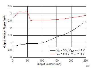
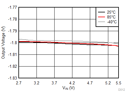
Unless otherwise specified, TA = 25°C, VIN = 5 V, and values for C1 to C4 are as shown in the 典型应用.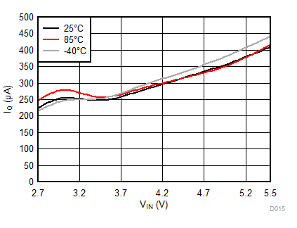
| EN = 1 | ILOAD = 0 mA |
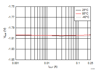
| VIN = 3 V | VOUT = –1.8 V | |
| R1 = 237 kΩ | R2 = 500 kΩ |
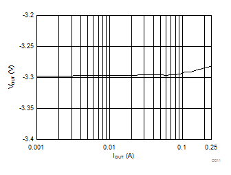
| VIN = 5 V | VOUT = –3.3 V | |
| R1 = 856 kΩ | R2 = 500 kΩ |
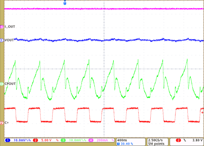
| VIN = 5.5 V | VOUT = –5 V | IOUT = 250 mA |
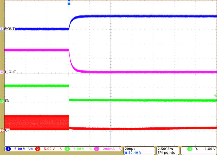
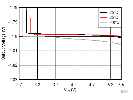
| VOUT = –1.8 | IOUT = 250 mA | R1 = 237 kΩ | R2 = 500 kΩ | |
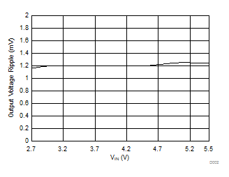
| VOUT = –1.8 V | IOUT = 100 mA |
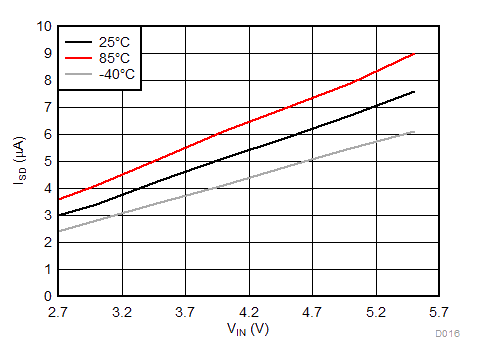
| EN = 0 |
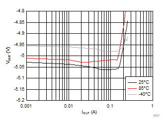
| VIN = 5.5 V | VOUT = –5 V | |
| R1 = 1.54 MΩ | R2 = 500 kΩ |
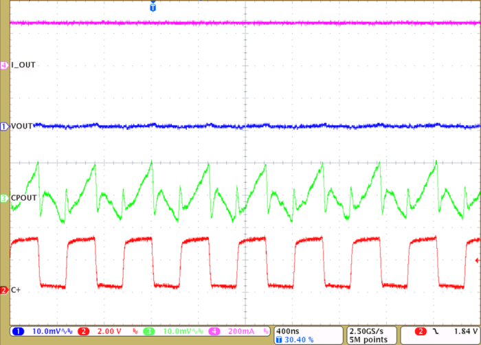
| VIN = 3 V | VOUT = –1.8 V | IOUT = 250 mA |
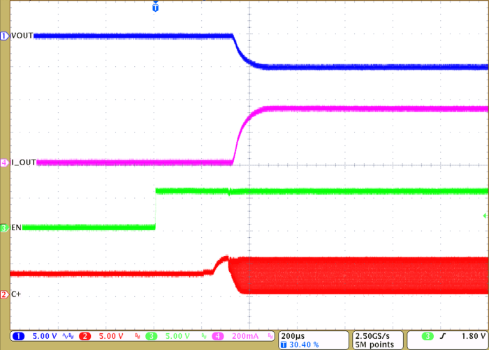
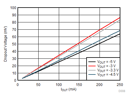
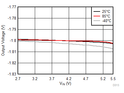
| VOUT = –1.8 V | IOUT = 100 mA | |
| R1 = 237 kΩ | R2 = 500 kΩ |
7 Detailed Description
7.1 Overview
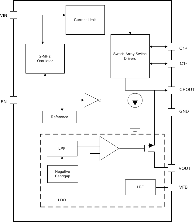
The LM27761 regulated charge-pump voltage converter inverts a positive voltage in the range of 2.7 V to 5.5 V to a negative voltage in the range of –1.5 V to –5 V. The negative LDO (low drop-out regulator), at the output of the charge-pump voltage converter, allows the device to provide a very low noise output, low output-voltage ripple, high PSRR, and low line and load transient responses. The output is externally configurable with gain-setting resistors. The LM27761 uses four low-cost capacitors to deliver up to 250 mA of output current.
7.2 Functional Block Diagram
7.3 Feature Description
7.3.1 Undervoltage Lockout
The LM27761 has an internal comparator that monitors the voltage at VIN and forces the device into shutdown if the input voltage drops to 2.4 V. If the input voltage rises above 2.6 V, the LM27761 resumes normal operation.
7.3.2 Input Current Limit
The LM27761 contains current limit circuitry that protects the device in the event of excessive input current and/or output shorts to ground. The input current is limited to 500 mA (typical) when the output is shorted directly to ground. When the LM27761 is current limiting, power dissipation in the device is likely to be quite high. In this event, thermal cycling is expected.
7.3.3 PFM Operation
To minimize quiescent current during light load operation, the LM27761 allows PFM or pulse-skipping operation. By allowing the charge pump to switch less when the output current is low, the quiescent current drawn from the power source is minimized. The frequency of pulsed operation is not limited and can drop into the sub-2-kHz range when unloaded. As the load increases, the frequency of pulsing increases until it transitions to constant frequency. The fundamental switching frequency in the LM27761 is 2 MHz.
7.3.4 Output Discharge
In shutdown, the LM27761 actively pulls down on the output of the device until the output voltage reaches GND. In this mode, the current drawn from the output is approximately 1.85 mA.
7.3.5 Thermal Shutdown
The LM27761 implements a thermal shutdown mechanism to protect the device from damage due to overheating. When the junction temperature rises to 150°C (typical), the device switches into shutdown mode. The LM27761 releases thermal shutdown when the junction temperature is reduced to 130°C (typical).
Thermal shutdown is most often triggered by self-heating, which occurs when there is excessive power dissipation in the device and/or insufficient thermal dissipation. The LM27761 device power dissipation increases with increased output current and input voltage. When self-heating brings on thermal shutdown, thermal cycling is the typical result. Thermal cycling is the repeating process where the part self-heats, enters thermal shutdown (where internal power dissipation is practically zero), cools, turns on, and then heats up again to the thermal shutdown threshold. Thermal cycling is recognized by a pulsing output voltage and can be stopped by reducing the internal power dissipation (reduce input voltage and/or output current) or the ambient temperature. If thermal cycling occurs under desired operating conditions, thermal dissipation performance must be improved to accommodate the power dissipation of the device.
7.4 Device Functional Modes
7.4.1 Shutdown Mode
An enable pin (EN) pin is available to disable the device and place the LM27761 into shutdown mode reducing the quiescent current to 7 µA. In shutdown, the output of the LM27761 is pulled to ground by an internal pullup current source (approximately 1.85 mA).
7.4.2 Enable Mode
Applying a voltage greater than 1.2 V to the EN pin brings the device into enable mode. When unloaded, the input current during operation is 370 µA. As the load current increases, so does the quiescent current. When enabled, the output voltage is equal to the inverse of the input voltage minus the voltage drop across the charge pump.
8 Application and Implementation
NOTE
Information in the following applications sections is not part of the TI component specification, and TI does not warrant its accuracy or completeness. TI’s customers are responsible for determining suitability of components for their purposes. Customers should validate and test their design implementation to confirm system functionality.
8.1 Application Information
The LM27761 low-noise charge-pump voltage converter inverts a positive voltage in the range of 2.7 V to 5.5 V to a negative output voltage configurable with external gain setting resistors. The device uses four low-cost capacitors to provide up to 250 mA of output current. The LM27761 operates at a 2-MHz oscillator frequency to reduce charge-pump output resistance and voltage ripple under heavy loads. With an operating current of only 370 µA and 7-µA typical shutdown current, the LM27761 provides ideal performance for battery-powered systems.
8.2 Typical Application - Regulated Voltage Inverter
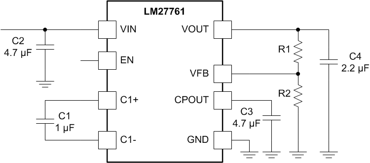
 Figure 16. LM27761 Typical Application
8.2.1 Design Requirements
Example requirements for typical applications using the LM27761 device are listed in Table 1:
Table 1. Design Parameters
| DESIGN PARAMETER | EXAMPLE VALUE |
|---|---|
| Input voltage | 2.7 V to 5.5 V |
| Output voltage | –1.5 V to –5 V |
| Output current | 0 mA to 250 mA |
| Boost switching frequency | 2 MHz |
8.2.2 Detailed Design Procedure
8.2.2.1 Custom Design With WEBENCH® Tools
Click here to create a custom design using the LM27761 device with the WEBENCH® Power Designer.
- Start by entering the input voltage (VIN), output voltage (VOUT), and output current (IOUT) requirements.
- Optimize the design for key parameters such as efficiency, footprint, and cost using the optimizer dial.
- Compare the generated design with other possible solutions from Texas Instruments.
The WEBENCH Power Designer provides a customized schematic along with a list of materials with real-time pricing and component availability.
In most cases, these actions are available:
- Run electrical simulations to see important waveforms and circuit performance
- Run thermal simulations to understand board thermal performance
- Export customized schematic and layout into popular CAD formats
- Print PDF reports for the design, and share the design with colleagues
Get more information about WEBENCH tools at www.ti.com/WEBENCH.
8.2.2.2 Charge-Pump Voltage Inverter
The main application of the LM27761 is to generate a regulated negative supply voltage. The voltage inverter circuit uses only three external capacitors, and the LDO regulator circuit uses one additional output capacitor.
The voltage inverter portion of the LM27761 contains four large CMOS switches which are switched in sequence to invert the input supply voltage. Energy transfer and storage are provided by external capacitors. Figure 17 shows the voltage switches S2 and S4 are open. In the second time interval, S1 and S3 are open; at the same time, S2 and S4 are closed, and C1 is charging C3. After a number of cycles, the voltage across C3 is pumped into VIN. Because the anode of C3 is connected to ground, the output at the cathode of C3 equals –(VIN) when there is no load current. When a load is added the output voltage dropis determined by the parasitic resistance (RDSON of the MOSFET switches and the equivalent series resistance (ESR) of the capacitors) and the charge transfer loss between the capacitors.
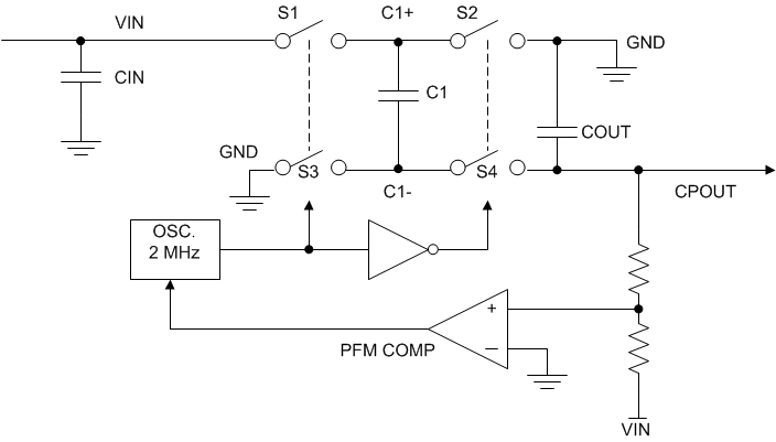 Figure 17. Voltage Inverting Principle
The output characteristic of this circuit can be approximated by an ideal voltage source in series with a resistance. The voltage source equals –(VIN). The output resistance ROUT is a function of the ON resistance of the internal MOSFET switches, the oscillator frequency, the capacitance, and the ESR of C1 and C3. Because the switching current charging and discharging C1 is approximately twice as the output current, the effect of the ESR of the pumping capacitor C1 is multiplied by four in the output resistance. The charge-pump output capacitor C3 is charging and discharging at a current approximately equal to the output current; therefore, its ESR only counts once in the output resistance. A good approximation of charge-pump ROUT is shown in Equation 1:
where
- RSW is the sum of the ON resistance of the internal MOSFET switches shown in Figure 17.
High capacitance and low-ESR ceramic capacitors reduce the output resistance.
8.2.2.3 Negative Low-Dropout Linear Regulator
At the output of the inverting charge-pump the LM27761 features a low-dropout, linear negative voltage regulator (LDO). The LDO output is rated for a current of 250 mA. This negative LDO allows the device to provide a very low noise output, low output voltage ripple, high PSRR, and low line or load transient response.
8.2.2.4 Power Dissipation
The allowed power dissipation for any package is a measure of the ability of the device to pass heat from the junctions of the device to the heatsink and the ambient environment. Thus, the power dissipation is dependent on the ambient temperature and the thermal resistance across the various interfaces between the die junction and ambient air.
The maximum allowable power dissipation can be calculated by Equation 2:
The actual power being dissipated in the device can be represented by Equation 3:
Equation 2 and Equation 3 establish the relationship between the maximum power dissipation allowed due to thermal consideration, the voltage drop across the device, and the continuous current capability of the device. These equations must be used to determine the optimum operating conditions for the device in a given application.
In lower power dissipation applications the maximum ambient temperature (TA-MAX) may be increased. In higher power dissipation applications the maximum ambient temperature(TA-MAX) may have to be derated. TA-MAX can be calculated using Equation 4:
where
- TJ-MAX-OP = maximum operating junction temperature (125°C)
- PD-MAX = the maximum allowable power dissipation
- RθJA = junction-to-ambient thermal resistance of the package
Alternately, if TA-MAX cannot be derated, the power dissipation value must be reduced. This can be accomplished by reducing the input voltage as long as the minimum VIN is not violated, or by reducing the output current, or some combination of the two.
8.2.2.5 Output Voltage Setting
The output voltage of the LM27761 is externally configurable. The value of R1 and R2 determines the output voltage setting. The output voltage can be calculated using Equation 5:
8.2.2.6 External Capacitor Selection
The LM27761 requires 4 external capacitors for proper operation. Surface-mount multi-layer ceramic capacitors are recommended. These capacitors are small, inexpensive, and have very low ESR (≤ 15 mΩ typical). Tantalum capacitors, OS-CON capacitors, and aluminum electrolytic capacitors generally are not recommended for use with the LM27761 due to their high ESR compared to ceramic capacitors.
For most applications, ceramic capacitors with an X7R or X5R temperature characteristic are preferable for use with the LM27761. These capacitors have tight capacitance tolerances (as good as ±10%) and hold their value over temperature (X7R: ±15% over –55°C to +125°C; X5R ±15% over –55°C to +85°C).
Using capacitors with a Y5V or Z5U temperature characteristic is generally not recommended for the LM27761. These capacitors typically have wide capacitance tolerance (80%, ….20%) and vary significantly over temperature (Y5V: 22%, –82% over –30°C to +85°C range; Z5U: 22%, –56% over 10°C to 85°C range). Under some conditions a 1-µF-rated Y5V or Z5U capacitor could have a capacitance as low as 0.1 µF. Such detrimental deviation is likely to cause Y5V and Z5U capacitors to fail to meet the minimum capacitance requirements of the LM27761.
Net capacitance of a ceramic capacitor decreases with increased DC bias. This degradation can result in lower-than-expected capacitance on the input and/or output, resulting in higher ripple voltages and currents. Using capacitors at DC bias voltages significantly below the capacitor voltage rating usually minimizes DC bias effects. Consult capacitor manufacturers for information on capacitor DC bias characteristics.
Capacitance characteristics can vary quite dramatically with different application conditions, capacitor types, and capacitor manufacturers. TI strongly recommends that the LM27761 circuit be evaluated thoroughly early in the design-in process with the mass-production capacitor of choice. This helps ensure that any such variability in capacitance does not negatively impact circuit performance.
8.2.2.6.1 Charge-Pump Output Capacitor
In typical applications, a 4.7-µF low-ESR ceramic charge-pump output capacitor (C3) is recommended. Different output capacitance values can be used to reduce charge pump ripple, shrink the solution size, and/or cut the cost of the solution. However, changing the output capacitor may also require changing the flying capacitor or input capacitor to maintain good overall circuit performance.
In higher-current applications, a 10-µF, 10-V low-ESR ceramic output capacitor is recommended. If a small output capacitor is used, the output ripple can become large during the transition between PFM mode and constant switching. To prevent toggling, a 2-µF capacitance is recommended. For example, 10-µF, 10-V output capacitor in a 0402 case size typically has only 2-µF capacitance when biased to 5 V.
8.2.2.6.2 Input Capacitor
The input capacitor (C2) is a reservoir of charge that aids in a quick transfer of charge from the supply to the flying capacitors during the charge phase of operation. The input capacitor helps to keep the input voltage from drooping at the start of the charge phase when the flying capacitors are connected to the input. It also filters noise on the input pin, keeping this noise out of the sensitive internal analog circuitry that is biased off the input line.
Input capacitance has a dominant and first-order effect on the input ripple magnitude. Increasing (decreasing) the input capacitance results in a proportional decrease (increase) in input voltage ripple. Input voltage, output current, and flying capacitance also affects input ripple levels to some degree.
In typical applications, a 4.7-µF low-ESR ceramic capacitor is recommended on the input. When operating near the maximum load of 250 mA, after taking into the DC bias derating, a minimum recommended input capacitance is 2 µF or larger. Different input capacitance values can be used to reduce ripple, shrink the solution size, and/or cut the cost of the solution.
8.2.2.6.3 Flying Capacitor
The flying capacitor (C1) transfers charge from the input to the output. Flying capacitance can impact both output current capability and ripple magnitudes. If flying capacitance is too small, the LM27761 may not be able to regulate the output voltage when load currents are high. On the other hand, if the flying capacitance is too large, the flying capacitor might overwhelm the input and charge pump output capacitors, resulting in increased input and output ripple.
In typical high-current applications, 0.47-µF or 1-µF 10-V low-ESR ceramic capacitors are recommended for the flying capacitors. Polarized capacitors (tantalum, aluminum, electrolytic, etc.) must not be used for the flying capacitor, as they could become reverse-biased during LM27761 operation.
8.2.2.6.4 LDO Output Capacitor
The LDO output capacitor (C4) value and the ESR affect stability, output ripple, output noise, PSRR and transient response. The LM27761 only requires the use of a 2.2-µF ceramic output capacitor for stable operation. For typical applications, a 2.2-µF ceramic output capacitor located close to the output is sufficient.
8.2.3 Application Curves
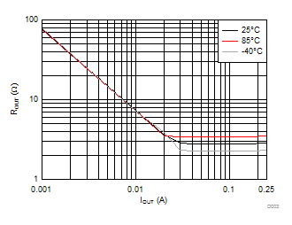
| VIN = 3 V | VOUT = –1.8 V |
Output Current
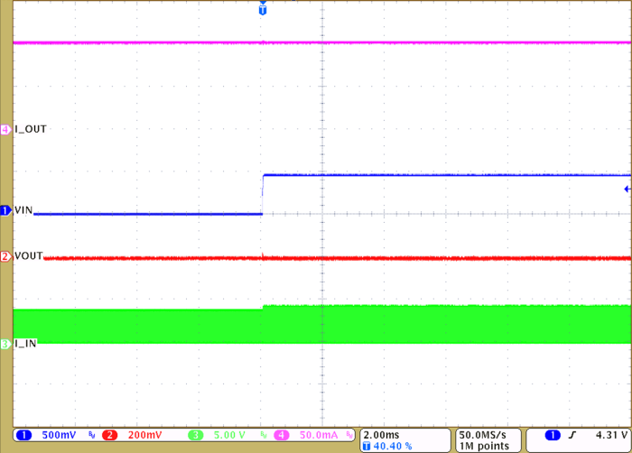
| VIN = 4V to 4.5 V | VOUT = –1.8 V | IOUT = 100 mA |
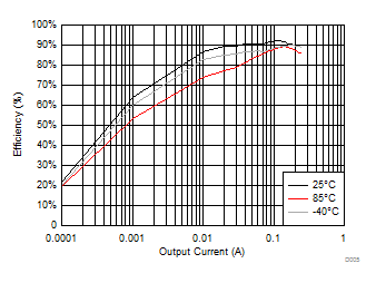
| VIN = 5.5 V | VOUT = –5 V | R1 = 1.54 MΩ | R2 = 500 kΩ | |
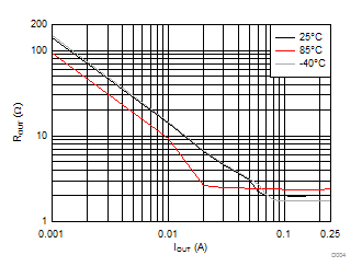
| VIN = 5.5 V | VOUT = –5 V |
Output Current
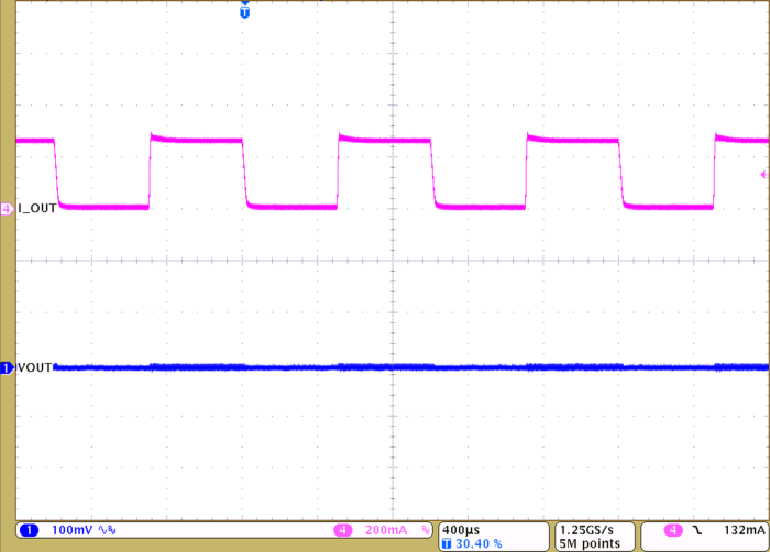
| VIN = 3 V | VOUT = –1.8 V |
9 Power Supply Recommendations
The LM27761 is designed to operate from an input voltage supply range between 2.7 V and 5.5 V. This input supply must be well regulated and capable of supplying the required input current. If the input supply is located far form the LM27761, additional bulk capacitance may be required in addition to the ceramic bypass capacitors.
10 Layout
10.1 Layout Guidelines
The high switching frequency and large switching currents of the LM27761 make the choice of layout important. Use the following steps as a reference to ensure the device is stable and maintains proper LED current regulation across its intended operating voltage and current range:
- Place CIN on the top layer (same layer as the LM27761) and as close to the device as possible. Connecting the input capacitor through short, wide traces to both the VIN and GND pins reduces the inductive voltage spikes that occur during switching which can corrupt the VIN line.
- Place CCPOUT on the top layer (same layer as the LM27761) and as close to the VOUT and GND pins as possible. The returns for both CIN and CCPOUT must come together at one point, as close to the GND pin as possible. Connecting CCPOUT through short, wide traces reduces the series inductance on the VCPOUT and GND pins that can corrupt the VCPOUT and GND lines and cause excessive noise in the device and surrounding circuitry.
- Place C1 on top layer (same layer as the LM27761) and as close to the device as possible. Connect the flying capacitor through short, wide traces to both the C1+ and C1– pins.
- Place COUT on the top layer (same layer as the LM27761) and as close to the VOUT pin as possible. For best performance the ground connection for COUT must connect back to the GND connection at the thermal pad of the device.
- Place R1 and R2 on the top layer (same layer as LM27761) and as close to the VFB pin as possible. For best performance the ground connection of R2 must connect back to the GND connection at the thermal pad of the device.
Connections using long trace lengths, narrow trace widths, or connections through vias must be avoided. These add parasitic inductance and resistance that results in inferior performance, especially during transient conditions.
10.2 Layout Example
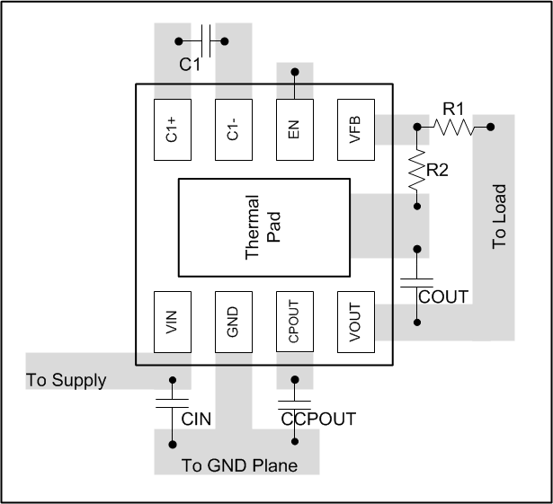 Figure 23. LM27761 Layout Example
11 器件和文档支持
11.1 器件支持
11.1.1 开发支持
11.1.1.1 使用 WEBENCH® 工具创建定制设计
请单击此处,使用 LM27761 器件并借助 WEBENCH® 电源设计器创建定制设计。
- 在开始阶段键入输出电压 (VIN)、输出电压 (VOUT) 和输出电流 (IOUT) 要求。
- 使用优化器拨盘优化关键设计参数,如效率、封装和成本。
- 将生成的设计与德州仪器 (TI) 的其他解决方案进行比较。
WEBENCH Power Designer 提供一份定制原理图以及罗列实时价格和组件可用性的物料清单。
在多数情况下,可执行以下操作:
- 运行电气仿真,观察重要波形以及电路性能
- 运行热性能仿真,了解电路板热性能
- 将定制原理图和布局方案导出至常用 CAD 格式
- 打印设计方案的 PDF 报告并与同事共享
有关 WEBENCH 工具的详细信息,请访问 www.ti.com/WEBENCH。
11.2 接收文档更新通知
要接收文档更新通知,请导航至德州仪器 TI.com.cn 上的器件产品文件夹。请单击右上角的通知我 进行注册,即可收到任意产品信息更改每周摘要。有关更改的详细信息,请查看任意已修订文档中包含的修订历史记录。
11.3 社区资源
下列链接提供到 TI 社区资源的连接。链接的内容由各个分销商“按照原样”提供。这些内容并不构成 TI 技术规范,并且不一定反映 TI 的观点;请参阅 TI 的 《使用条款》。
-
TI E2E™ 在线社区 TI 的工程师对工程师 (E2E) 社区。此社区的创建目的在于促进工程师之间的协作。在 e2e.ti.com 中,您可以咨询问题、分享知识、拓展思路并与同行工程师一道帮助解决问题。
-
设计支持 TI 参考设计支持 可帮助您快速查找有帮助的 E2E 论坛、设计支持工具以及技术支持的联系信息。
11.4 商标
E2E is a trademark of Texas Instruments.
WEBENCH is a registered trademark of Texas Instruments.
All other trademarks are the property of their respective owners.
11.5 静电放电警告

这些装置包含有限的内置 ESD 保护。 存储或装卸时,应将导线一起截短或将装置放置于导电泡棉中,以防止 MOS 门极遭受静电损伤。
11.6 Glossary
SLYZ022 — TI Glossary.
This glossary lists and explains terms, acronyms, and definitions.
12 机械、封装和可订购信息
以下页面包括机械、封装和可订购信息。这些信息是指定器件的最新可用数据。这些数据发生变化时,我们可能不会另行通知或修订此文档。如欲获取此产品说明书的浏览器版本,请参阅左侧的导航栏。
重要声明
德州仪器(TI) 及其下属子公司有权根据 JESD46 最新标准, 对所提供的产品和服务进行更正、修改、增强、改进或其它更改, 并有权根据 JESD48最新标准中止提供任何产品和服务。客户在下订单前应获取最新的相关信息, 并验证这些信息是否完整且是最新的。所有产品的销售都遵循在订单确认时所提供的TI 销售条款与条件。
TI 保证其所销售的组件的性能符合产品销售时 TI 半导体产品销售条件与条款的适用规范。仅在 TI 保证的范围内,且 TI 认为有必要时才会使用测试或其它质量控制技术。除非适用法律做出了硬性规定,否则没有必要对每种组件的所有参数进行测试。
TI 对应用帮助或客户产品设计不承担任何义务。客户应对其使用 TI 组件的产品和应用自行负责。为尽量减小与客户产品和应用相关的风险,客户应提供充分的设计与操作安全措施。
TI 不对任何 TI 专利权、版权、屏蔽作品权或其它与使用了 TI 组件或服务的组合设备、机器或流程相关的 TI 知识产权中授予 的直接或隐含权限作出任何保证或解释。TI所发布的与第三方产品或服务有关的信息,不能构成从 TI 获得使用这些产品或服 务的许可、授权、或认可。使用此类信息可能需要获得第三方的专利权或其它知识产权方面的许可,或是 TI 的专利权或其它知识产权方面的许可。
对于 TI 的产品手册或数据表中 TI 信息的重要部分,仅在没有对内容进行任何篡改且带有相关授权、条件、限制和声明的情况 下才允许进行复制。TI 对此类篡改过的文件不承担任何责任或义务。复制第三方的信息可能需要服从额外的限制条件。
在转售 TI 组件或服务时,如果对该组件或服务参数的陈述与 TI 标明的参数相比存在差异或虚假成分,则会失去相关 TI 组件或服务的所有明示或暗示授权,且这是不正当的、欺诈性商业行为。TI 对任何此类虚假陈述均不承担任何责任或义务。
客户认可并同意,尽管任何应用相关信息或支持仍可能由 TI 提供,但他们将独力负责满足与其产品及在其应用中使用 TI 产品相关的所有法律、法规和安全相关要求。客户声明并同意,他们具备制定与实施安全措施所需的全部专业技术和知识,可预见故障的危险后果、监测故障及其后果、降低有可能造成人身伤害的故障的发生机率并采取适当的补救措施。客户将全额赔偿因 在此类安全关键应用中使用任何 TI 组件而对 TI及其代理造成的任何损失。
在某些场合中,为了推进安全相关应用有可能对 TI 组件进行特别的促销。TI 的目标是利用此类组件帮助客户设计和创立其特有的可满足适用的功能安全性标准和要求的终端产品解决方案。尽管如此,此类组件仍然服从这些条款。
TI 组件未获得用于 FDA Class III(或类似的生命攸关医疗设备)的授权许可,除非各方授权官员已经达成了专门管控此类使 用的特别协议。
只有那些 TI 特别注明属于军用等级或“增强型塑料”的 TI 组件才是设计或专门用于军事/航空应用或环境的。购买者认可并同 意,对并非指定面向军事或航空航天用途的 TI组件进行军事或航空航天方面的应用,其风险由客户单独承担,并且由客户独 力负责满足与此类使用相关的所有法律和法规要求。
TI 已明确指定符合 ISO/TS16949 要求的产品,这些产品主要用于汽车。在任何情况下,因使用非指定产品而无法达到 ISO/TS16949要求,TI不承担任何责任。
产品
- 数字音频: www.ti.com.cn/audio
- 放大器和线性器件: www.ti.com.cn/amplifiers
- 数据转换器: www.ti.com.cn/dataconverters
- DLP® 产品: www.dlp.com
- DSP - 数字信号处理器: www.ti.com.cn/dsp
- 时钟和计时器: www.ti.com.cn/clockandtimers
- 接口: www.ti.com.cn/interface
- 逻辑: www.ti.com.cn/logic
- 电源管理: www.ti.com.cn/power
- 微控制器 (MCU): www.ti.com.cn/microcontrollers
- RFID 系统: www.ti.com.cn/rfidsys
- OMAP应用处理器: www.ti.com/omap
- 无线连通性: www.ti.com.cn/wirelessconnectivity
应用
- 通信与电信: www.ti.com.cn/telecom
- 计算机及周边: www.ti.com.cn/computer
- 消费电子: www.ti.com/consumer-apps
- 能源: www.ti.com/energy
- 工业应用: www.ti.com.cn/industrial
- 医疗电子: www.ti.com.cn/medical
- 安防应用: www.ti.com.cn/security
- 汽车电子: www.ti.com.cn/automotive
- 视频和影像: www.ti.com.cn/video
德州仪器在线技术支持社区: www.deyisupport.com
邮寄地址: 上海市浦东新区世纪大道1568 号,中建大厦32 楼邮政编码: 200122
Copyright© 2016, 德州仪器半导体技术(上海)有限公司
