-
TUSB320LAI/TUSB320HAI USB Type-C 配置通道逻辑和端口控制 ZHCSEB3D October 2015 – May 2017 TUSB320HAI , TUSB320LAI
PRODUCTION DATA.
-
TUSB320LAI/TUSB320HAI USB Type-C 配置通道逻辑和端口控制
- 1 特性
- 2 应用
- 3 说明
- 4 修订历史记录
- 5 Pin Configuration and Functions
- 6 Specifications
- 7 Detailed Description
- 8 Application and Implementation
- 9 Power Supply Recommendations
- 10Layout
- 11器件和文档支持
- 12机械、封装和可订购信息
- 重要声明
TUSB320LAI/TUSB320HAI USB Type-C 配置通道逻辑和端口控制
1 特性
- USB Type-C™规范 1.1
- 向后兼容 USB Type-C 规范 1.0
- 支持高达 3A 的电流通告和检测
- 模式配置
- 仅主机 - 下行端口 (DFP)(供电设备)
- 仅设备 – 上行端口 (UFP)(受电设备)
- 双角色端口 – DRP
- 支持 Try.SRC 和 Try.SNK
- 通道配置 (CC)
- USB 端口连接检测
- 电缆方向检测
- 角色检测
- Type-C 电流模式(默认、中等和高)
- VBUS 检测
- I2C 或 GPIO 控制
- 支持频率高达 400kHz 的 I2C
- 通过 I2C 实现角色配置控制
- 电源电压:2.7V 至 5V
- 低电流消耗
- 工业温度范围:–40°C 至 85°C
2 应用
- 主机、设备、双角色端口 应用
- 移动电话
- 平板电脑和笔记本电脑
- USB 外设
3 说明
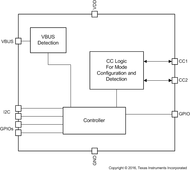
除非另外注明,否则 TUSB320LA 和 TUSB320HA 器件(以下简称为 TUSB320)为德州仪器 (TI) 的第三代 Type-C 配置通道逻辑和端口控制器。TUSB320 器件使用 CC 引脚来确定端口的连接状态和电缆方向,以及进行角色检测和 Type-C 电流模式控制。TUSB320 器件可配置为下行端口 (DFP)、上行端口 (UFP) 或双角色端口 (DRP),因此成为各种应用的理想选择。
根据 Type-C 规范,TUSB320 器件会交替配置为 DFP 或 UFP。CC 逻辑块通过监视 CC1 和 CC2 引脚上的上拉或下拉电阻,以确定何时连接了 USB 端口、电缆的方向以及检测到的角色。CC 逻辑根据检测到的角色来确定 Type-C 电流模式为默认、中等还是高。该逻辑通过实施 VBUS 检测来确定端口在 UFP 和 DRP 模式下是否连接成功。
该系列器件能够在宽电源范围内工作,并且具有较低功耗。TUSB320 提供两种使能版本:低电平有效使能,称为 TUSB320LA;高电平有效使能,称为 TUSB320HA。TUSB320 系列器件适用于工业级温度范围。
器件信息(1)
| 器件型号 | 封装 | 封装尺寸(标称值) |
|---|---|---|
| TUSB320LAI | X2QFN (12) | 1.60mm x 1.60mm |
| TUSB320HAI | X2QFN (12) | 1.60mm x 1.60mm |
- 如需了解所有可用封装,请参阅产品说明书末尾的可订购产品附录。
简化电路原理图
示例 应用

4 修订历史记录
Changes from C Revision (October 2016) to D Revision
- Changed RVBUS values From: MIN = 891, TYP = 900, MAX = 909 KΩ To: MIN = 855, TYP = 887, MAX = 920 KΩ Go
Changes from B Revision (September 2016) to C Revision
- Changed text for Pin 7 in the Pin Functions table From: "default current mode detected (H); medium or high current mode detected (L)." To: "Refer to Table 3 for more details." Go
- Changed text for Pin 8 in the Pin Functions table From: "default or medium current mode detected (H); high current mode detected (L)." To: "Refer to Table 3 for more details." Go
Changes from A Revision (March 2016) to B Revision
- Changed pins CC1 and CC2 values From: MIN = –0.3 MAX = VDD + 0.3 To: MIN –0.3 MAX = 6 in the Absolute Maximum RatingsGo
Changes from * Revision (October 2015) to A Revision
- Added Note 1 and 2 to the Pin Functions tableGo
- Changed the DESCRIPTION of pin EN_N pin in the Pin Functions tableGo
- Changed the DESCRIPTION of pin EN pin in the Pin Functions tableGo
- Changed the DESCRIPTION of pin VDD in the Pin Functions tableGo
- Added Test Condition "See Figure 1" to VBUS_THR in the Electrical Characteristics Go
- Added Note 2 to the Electrical Characteristics table Go
- Changed the last sentence of the Debug Accessory sectionGo
- Added Note: "SW must make sure..." to the Description of INTERRUPT_STATUS in Table 9 Go
- Added text to list item 2 in the TUSB320LA Initialization Procedure sectionGo
- Added text to list item 2 in the TUSB320HA Initialization Procedure sectionGo
5 Pin Configuration and Functions
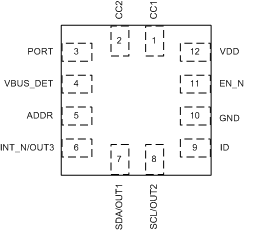
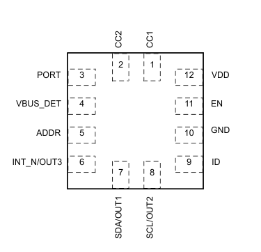
Pin Functions
| PIN | TYPE | DESCRIPTION | ||
|---|---|---|---|---|
| NAME | TUSB320LA | TUSB320HA | ||
| CC1 | 1 | 1 | I/O | Type-C configuration channel signal 1 |
| CC2 | 2 | 2 | I/O | Type-C configuration channel signal 2 |
| PORT(1) | 3 | 3 | I | Tri-level input pin to indicate port mode. The state of this pin is sampled when EN_N is asserted low in the TUSB320L device, EN is asserted high in the TUSB320H device, and VDD is active. This pin is also sampled following a I2C_SOFT_RESET. H - DFP (Pull-up to VDD if DFP mode is desired) NC - DRP (Leave unconnected if DRP mode is desired) L - UFP (Pull-down or tie to GND if UFP mode is desired) |
| VBUS_DET(1) | 4 | 4 | I | 5-V to 28-V VBUS input voltage. VBUS detection determines UFP attachment. One 900-kΩ external resistor required between system VBUS and VBUS_DET pin. |
| ADDR(1) | 5 | 5 | I | Tri-level input pin to indicate I2C address or GPIO mode: H — I2C is enabled and I2C 7-bit address is 0x67. NC — GPIO mode (I2C is disabled) L — I2C is enabled and I2C 7-bit address is 0x47. ADDR pin should be pulled up to VDD if high configuration is desired |
| INT_N/OUT3(1) | 6 | 6 | O | The INT_N/OUT3 is a dual-function pin. When used as the INT_N, the pin is an open drain output in I2C control mode and is an active low interrupt signal for indicating changes in I2C registers. When used as OUT3, the pin is in audio accessory detect in GPIO mode: no detection (H), audio accessory connection detected (L). |
| SDA/OUT1(1)(2) | 7 | 7 | I/O | The SDA/OUT1 is a dual-function pin. When I2C is enabled (ADDR pin is high or low), this pin is the I2C communication data signal. When in GPIO mode (ADDR pin is NC), this pin is an open drain output for communicating Type-C current mode detect when the device is in UFP mode: Refer to Table 3 for more details. |
| SCL/OUT2(1)(2) | 8 | 8 | I/O | The SCL/OUT2 is a dual function pin. When I2C is enabled (ADDR pin is high or low), this pin is the I2C communication clock signal. When in GPIO mode (ADDR pin is NC), this pin is an open drain output for communicating Type-C current mode detect when the device is in UFP mode: Refer to Table 3 for more details. |
| ID | 9 | 9 | O | Open drain output; asserted low when the CC pins detect device attachment when port is a source (DFP), or dual-role (DRP) acting as source (DFP). |
| GND | 10 | 10 | G | Ground |
| EN_N | 11 | — | I | Enable signal; active low. Pulled up to VDD internally to disable the TUSB320L device. If controlled externally, must be held low at least for 50 ms after VDD has reached its valid voltage level. |
| EN | — | 11 | I | Enable signal; active high. Pulled down to GND internally to disable the TUSB320H device. If controlled externally, must be held low at least for 50 ms after VDD has reached its valid voltage level. |
| VDD | 12 | 12 | P | Positive supply voltage. VDD must ramp within 25 ms or less |
6 Specifications
6.1 Absolute Maximum Ratings
over operating free-air temperature range (unless otherwise noted)(1)6.2 ESD Ratings
| VALUE | UNIT | |||
|---|---|---|---|---|
| V(ESD) | Electrostatic discharge | Human-body model (HBM), per ANSI/ESDA/JEDEC JS-001(1) | ±3000 | V |
| Charged-device model (CDM), per JEDEC specification JESD22-C101(2) | ±1500 | |||
6.3 Recommended Operating Conditions
over operating free-air temperature range (unless otherwise noted)| MIN | NOM | MAX | UNIT | ||
|---|---|---|---|---|---|
| VDD | Supply voltage range | 2.7 | 5 | V | |
| VBUS | System VBUS voltage | 4 | 5 | 28 | V |
| TA | TUSB320HAI and TUSB320LAI Operating free air temperature range | –40 | 25 | 85 | °C |
6.4 Thermal Information
| THERMAL METRIC(1) | TUSB320 | UNIT | |
|---|---|---|---|
| RWB (X2QFN) | |||
| 12 PINS | |||
| RθJA | Junction-to-ambient thermal resistance | 169.3 | °C/W |
| RθJC(top) | Junction-to-case (top) thermal resistance | 68.1 | °C/W |
| RθJB | Junction-to-board thermal resistance | 83.4 | °C/W |
| ψJT | Junction-to-top characterization parameter | 2.2 | °C/W |
| ψJB | Junction-to-board characterization parameter | 83.4 | °C/W |
| RθJC(bot) | Junction-to-case (bottom) thermal resistance | N/A | |
6.5 Electrical Characteristics
over operating free-air temperature range (unless otherwise noted)| PARAMETER | TEST CONDITIONS | MIN | TYP | MAX | UNIT | |
|---|---|---|---|---|---|---|
| POWER CONSUMPTION | ||||||
| IUNATTACHED_UFP | Current consumption in unattached mode when port is unconnected and waiting for connection. [VDD = 4.5 V, EN_N (TUSB320LA) = L, EN (TUSB320HA) = H, ADDR = NC, PORT = L] | 70 | µA | |||
| IACTIVE_UFP | Current consumption in active mode. [VDD = 4.5 V, EN_N (TUSB320LA) = L, EN (TUSB320HA) = H, ADDR = NC, PORT = L] | 70 | µA | |||
| ISHUTDOWN | Leakage current when VDD is supplied, but the TUSB320 device is not enabled. [VDD = 4.5 V, EN_N (TUSB320LA) = H, EN (TUSB320HA) = L] | 0.04 | µA | |||
| CC1 AND CC2 PINS | ||||||
| RCC_DB | Pulldown resistor when in dead-battery mode. | 4.1 | 5.1 | 6.1 | kΩ | |
| RCC_D | Pulldown resistor when in UFP or DRP mode. | 4.6 | 5.1 | 5.6 | kΩ | |
| VUFP_CC_USB | Voltage level range for detecting a DFP attach when configured as a UFP and DFP is advertising default current source capability. | 0.25 | 0.61 | V | ||
| VUFP_CC_MED | Voltage level range for detecting a DFP attach when configured as a UFP and DFP is advertising medium (1.5-A) current source capability. | 0.7 | 1.16 | V | ||
| VUFP_CC_HIGH | Voltage level range for detecting a DFP attach when configured as a UFP and DFP is advertising high (3-A) current source capability. | 1.31 | 2.04 | V | ||
| VTH_DFP_CC_USB | Voltage threshold for detecting a UFP attach when configured as a DFP and advertising default current source capability. | 1.51 | 1.6 | 1.64 | V | |
| VTH_DFP_CC_MED | Voltage threshold for detecting a UFP attach when configured as a DFP and advertising medium current (1.5-A) source capability. | 1.51 | 1.6 | 1.64 | V | |
| VTH_DFP_CC_HIGH | Voltage threshold for detecting a UFP attach when configured as a DFP and advertising high current (3.0-A) source capability. | 2.46 | 2.6 | 2.74 | V | |
| ICC_DEFAULT_P | Default mode pullup current source when operating in DFP or DRP mode. | 64 | 80 | 96 | µA | |
| ICC_MED_P | Medium (1.5-A) mode pullup current source when operating in DFP or DRP mode. | 166 | 180 | 194 | µA | |
| ICC_HIGH_P | High (3-A) mode pullup current source when operating in DFP or DRP mode.(1) | 304 | 330 | 356 | µA | |
| CONTROL PINS: PORT, ADDR, INT/OUT3, EN_N, EN, ID | ||||||
| VIL | Low-level control signal input voltage (PORT, ADDR, EN_N, EN) | 0.4 | V | |||
| VIM | Mid-level control signal input voltage (PORT, ADDR) | 0.28 × VDD | 0.56 × VDD | V | ||
| VIH | High-level control signal input voltage (PORT, ADDR, EN_N) | VDD – 0.3 | VDD | V | ||
| VIH_EN | High-Level control signal input voltage for EN for TUSB320HA | 1.05 | 3.65 | V | ||
| IIH | High-level input current | –20 | 20 | µA | ||
| IIL | Low-level input current | –10 | 10 | µA | ||
| IID_LEAKAGE | Current Leakage on ID pin | VDD = 0 V; ID = 5 V | 10 | µA | ||
| REN_N | Internal pullup resistance for EN_N for TUSB320LA | 1.1 | MΩ | |||
| REN | Internal pulldown resistance for EN for TUSB320HA | 500 | kΩ | |||
| Rpu(2) | Internal pullup resistance (PORT, ADDR) | 588 | kΩ | |||
| Rpd (2) | Internal pulldown resistance (PORT, ADDR) | 1.1 | MΩ | |||
| VOL | Low-level signal output voltage (open-drain) (INT_N/OUT3, ID) | IOL = –1.6 mA | 0.4 | V | ||
| Rp_ODext | External pullup resistor on open drain IOs (INT_N/OUT3, ID) | 200 | kΩ | |||
| Rp_TLext | Tri-level input external pullup resistor (PORT, ADDR) | 4.7 | kΩ | |||
| I2C - SDA/OUT1, SCL/OUT2 CAN OPERATE FROM 1.8 V OR 3.3 V (±10%)(3) | ||||||
| VDD_I2C | Supply range for I2C (SDA/OUT1, SCL/OUT2) | 1.65 | 1.8 | 3.6 | V | |
| VIH | High-level signal voltage | 1.05 | 3.6 | V | ||
| VIL | Low-level signal voltage | 0.4 | V | |||
| VOL | Low-level signal output voltage (open drain) | IOL = –1.6 mA | 0.4 | V | ||
| VBUS_DET IO PINS (CONNECTED TO SYSTEM VBUS SIGNAL) | ||||||
| VBUS_THR | VBUS threshold range | See Figure 1 | 2.95 | 3.3 | 3.8 | V |
| RVBUS | External resistor between VBUS and VBUS_DET pin | 855 | 887 | 920 | KΩ | |
| RVBUS_PD | Internal pulldown resistance for VBUS_DET | 95 | KΩ | |||
6.6 Timing Requirements
| MIN | NOM | MAX | UNIT | ||
|---|---|---|---|---|---|
| I2C (SDA, SCL) | |||||
| tSU:DAT | Data setup time | 100 | ns | ||
| tHD;DAT | Data hold time | 10 | ns | ||
| tSU:STA | Set-up time, SCL to start condition | 0.6 | µs | ||
| tHD:STA | Hold time (repeated), start condition to SCL | 0.6 | µs | ||
| tSU:STO | Set up time for stop condition | 0.6 | µs | ||
| tBUF | Bus free time between a stop and start condition | 1.3 | µs | ||
| tVD;DAT | Data valid time | 0.9 | µs | ||
| tVD;ACK | Data valid acknowledge time | 0.9 | µs | ||
| fSCL | SCL clock frequency; I2C mode for local I2C control | 400 | kHz | ||
| tr | Rise time of both SDA and SCL signals | 300 | ns | ||
| tf | Fall time of both SDA and SCL signals | 300 | ns | ||
| CBUS_100KHZ | Total capacitive load for each bus line when operating at ≤ 100 kHz | 400 | pF | ||
| CBUS_400KHz | Total capacitive load for each bus line when operating at 400 kHz | 100 | pF | ||
6.7 Switching Characteristics
over operating free-air temperature range (unless otherwise noted)| PARAMETER | TEST CONDITIONS | MIN | TYP | MAX | UNIT | |
|---|---|---|---|---|---|---|
| tCCCB_DEFAULT | Power on default of CC1 and CC2 voltage debounce time | DEBOUCE register = 2'b00 |
168 | ms | ||
| tVBUS_DB | Debounce of VBUS_DET pin after valid VBUS_THR | 2 | ms | |||
| tDRP_DUTY_CYCLE | Power-on default of percentage of time DRP advertises DFP during a tDRP | DRP_DUTY_CYCLE register = 2'b00 |
30% | |||
| tDRP | The period during which the TUSB320HA or the TUSB320LA in DFP mode completes a DFP to UFP and back advertisement. | 50 | 75 | 100 | ms | |
| tI2C_EN | Time from TUSB320LA EN_N low or TUSB320HA EN high and VDD active to I2C access available | 100 | ms | |||
| tSOFT_RESET | Soft reset duration | 26 | 49 | 95 | ms | |
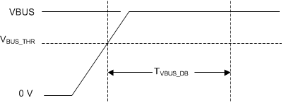 Figure 1. VBUS Detect and Debounce
7 Detailed Description
7.1 Overview
The USB Type-C ecosystem operates around a small form factor connector and cable that is flippable and reversible. Because of the nature of the connector, a scheme is required to determine the connector orientation. Additional schemes are required to determine when a USB port is attached and what the acting role of the USB port (DFP, UFP, DRP) is, as well as to communicate Type-C current capabilities. These schemes are implemented over the CC pins according to the USB Type-C pecification. The TUSB320 devices provide Configuration Channel (CC) logic for determining USB port attach and detach, role detection, cable orientation, and Type-C current mode. The TUSB320 devices also contains several features such as mode configuration and low standby current which make these devices ideal for source or sinks in USB2.0 applications.
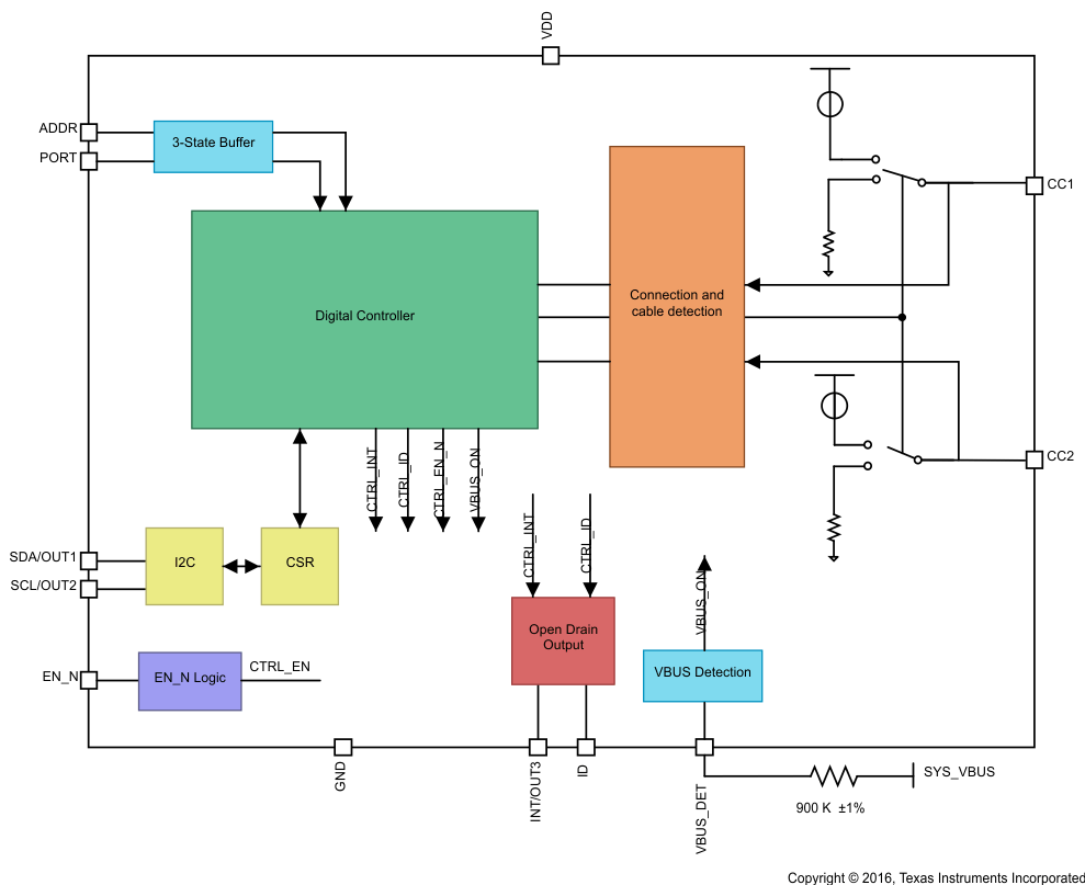 Figure 2. Functional Block Diagram of TUSB320
7.1.1 Cables, Adapters, and Direct Connect Devices
Type-C specification defines several cables, plugs, and receptacles to be used to attach ports. The TUSB320 devices support all cables, receptacles, and plugs. The TUSB320 devices do not support any USB Type-C feature which requires USB power delivery communication over CC lines like e-marking or alternate mode.
7.1.1.1 USB Type-C Receptacles and Plugs
Below is list of Type-C receptacles and plugs supported by the TUSB320 devices:
- USB Type-C receptacle for USB2.0 platforms and devices
- USB full-featured Type-C plug
- USB2.0 Type-C plug
7.1.1.2 USB Type-C Cables
Below is a list of Type-C cables types supported by the TUSB320 devices:
- USB full-featured Type-C cable
- USB2.0 Type-C cable with USB2.0 plug
- Captive cable on remote device with either a USB full-featured plug or USB2.0 plug
7.1.1.3 Legacy Cables and Adapters
The TUSB320 devices support legacy cable adapters as defined by the Type-C specification. The cable adapter must correspond to the mode configuration of a TUSB320 device.
Figure 3 displays the TUSB320 Legacy Adapter Implementation Circuit.
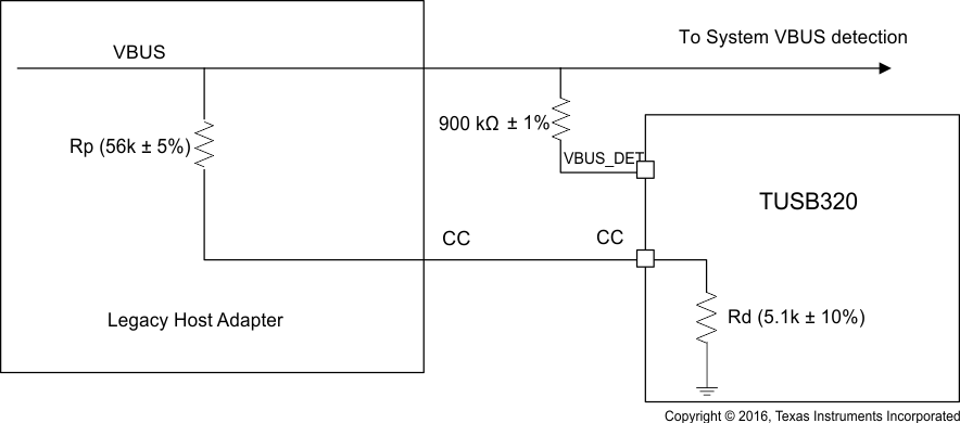 Figure 3. Legacy Adapter Implementation Circuit
7.1.1.4 Direct Connect Devices
The TUSB320 devices support the attaching and detaching of a direct-connect device.
7.1.1.5 Audio Adapters
Additionally, the TUSB320 devices support audio adapters for audio accessory mode, including:
- Passive Audio Adapter
- Charge Through Audio Adapter
7.2 Feature Description
7.2.1 Port Role Configuration
The TUSB320 devices can be configured as a downstream facing port (DFP), upstream facing port (UFP), or dual-role port (DRP) using the tri-level PORT pin. The PORT pin should be pulled high to VDD using a pullup resistance, low to GND or left as floated on the PCB to achieve the desired mode. This flexibility allows a TUSB320 device to be used in a variety of applications. A TUSB320 device samples the PORT pin after reset and maintains the desired mode until the TUSB320 device is reset again. The port role can also be selected through I2C registers. Table 1 lists the supported features in each mode:
Table 1. Supported Features for the TUSB320 Device by Mode
| PORT PIN | HIGH (DFP ONLY) |
LOW (UFP ONLY) |
NC (DRP) |
|---|---|---|---|
| SUPPORTED FEATURES | |||
| Port attach and detach | Yes | Yes | Yes |
| Cable orientation (through I2C) | Yes | Yes | Yes |
| Current advertisement | Yes | - | Yes (DFP) |
| Current detection | - | Yes | Yes (UFP) |
| Accessory modes (audio and debug) | Yes | Yes | Yes |
| Try.SRC | - | - | Yes |
| Try.SNK | - | - | Yes |
| Active cable detection | Yes | - | Yes (DFP) |
| I2C / GPIO | Yes | Yes | Yes |
| Legacy cables | Yes | Yes | Yes |
| VBUS detection | - | Yes | Yes (UFP) |
7.2.1.1 Downstream Facing Port (DFP) - Source
The TUSB320 device can be configured as a DFP-only by pulling the PORT pin high through a resistance to VDD or by changing the MODE_SELECT register. In DFP-only mode, the TUSB320 device constantly presents Rps on both CC. In DFP-only mode, the TUSB320 device initially advertises default USB Type-C current. The Type-C current can be adjusted through I2C if the system requires to increase the amount advertised. The TUSB320 device adjusts the Rps to match the desired Type-C current advertisement. In GPIO mode, the TUSB320 device only advertises default Type-C current.
When configured as a DFP, the TUSB320 device can operate with older USB Type-C 1.0 devices except for a USB Type-C 1.0 DRP device. A USB Type-C 1.1 compliant DFP can not connect to a Type-C 1.0 DRP. Because the TUSB320 device is compliant to Type-C 1.1, the TUSB320 device can not operate with a USB Type-C 1.0 DRP device. This limitation is a result of a backwards compatibility problem between USB Type-C 1.1 DFP and a USB Type-C 1.0 DRP.
7.2.1.2 Upstream Facing Port (UFP) - Sink
The TUSB320 device can be configured as a UFP only by pulling the PORT pin low to GND. In UFP mode, the TUSB320 device constantly presents pulldown resistors (Rd) on both CC pins. The TUSB320 device monitors the CC pins for the voltage level corresponding to the Type-C mode current advertisement by the connected DFP. The TUSB320 device debounces the CC pins and wait for VBUS detection before successfully attaching. As a UFP, the TUSB320 device detects and communicates the advertised current level of the DFP to the system through the OUT1 and OUT2 GPIOs (if in GPIO mode) or through the I2C CURRENT_MODE_DETECT register one time in the Attached.SNK state.
7.2.1.3 Dual Role Port (DRP)
The TUSB320 device can be configured to operate as a DRP when the PORT pin is left floated on the PCB. In DRP mode, the TUSB320 device toggles between operating as a DFP and a UFP. When functioning as a DFP in DRP mode, the TUSB320 device complies with all operations as defined for a DFP according to the Type-C specification. When presenting as a UFP in DRP mode, the TUSB320 device operates as defined for a UFP according to the Type-C specification.
The TUSB320 supports two optional Type-C DRP features called Try.SRC and Try.SNK. Products supporting dual-role functionality may have a requirement to be a source (DFP) or a sink (UFP) when connected to another dual-role capable product. For example, a dual-role capable notebook can be a source when connected to a tablet, or a cell phone can be a sink when connected to a notebook or tablet. When standard DRP products (products which don’t support either Try.SRC or Try.SNK) are connected together, the role (UFP or DFP) outcome is not predetermined. These two optional DRP features provide a means for dual-role capable products to connect to another dual-role capable product in the role desired. Try.SRC and Try.SNK are only available when TUSB320 is configured in I2C mode. When operating in GPIO mode, the TUSB320 will always operate as a standard DRP.
The Try.SRC feature of the TUSB320 device provides a means for a DRP product to connect as a DFP when connected to another DRP product that doesn’t implement Try.SRC. When two products which implement Try.SRC are connected together, the role outcome of either UFP or DFP is the same as a standard DRP. Try.SRC is enabled by changing I2C register SOURCE_PREF to 2’b11. Once this register is changed to 2’b11, the TUSB320 will always attempt to connect as a DFP when attached to another DRP capable device.
The Try.SNK feature of the TUSB320 device provides a method for a DRP product to connect as a UFP when connected to another DRP product that doesn’t implement Try.SNK. When two products which implement Try.SNK are connected together, the role outcome of either UFP or DFP is the same as a standard DRP. Try.SNK is enabled by changing I2C register SOURCE_PREF to 2’b01. Once this register is changed to 2’b01, the TUSB320 will always attempt to connect as a UFP when attached to another DRP capable device.
7.2.2 Type-C Current Mode
When a valid cable detection and attach have been completed, the DFP has the option to advertise the level of Type-C current a UFP can sink. The default current advertisement for the TUSB320 device is max of 500 mA (for USB2.0) or max of 900 mA (for USB3.1). If a higher level of current is available, the I2C registers can be written to provide medium current at 1.5 A or high current at 3 A. When the CURRENT_MODE_ADVERTISE register has been written to advertise higher than default current, the DFP adjusts the Rps for the specified current level. If a DFP advertises 3 A, system designer must ensure that the VDD of the TUSB320 device is 3.5 V or greater. Table 2 lists the Type-C current advertisements in GPIO an I2C modes.
Table 2. Type-C Current Advertisement for GPIO and I2C Modes
| TYPE-C CURRENT | GPIO MODE (ADDR PIN IN NC) | I2C MODE (ADDR PIN H, L) | |||
|---|---|---|---|---|---|
| UFP (PORT PIN L) | DFP (PORT PIN H) | UFP | DFP | ||
| Default | max of 500 mA (USB2.0) max of 900 mA (USB3.1) |
Current mode detected and output through OUT1 / OUT2 | Only advertisement | Current mode detected and read through I2C register | I2C register default is 500 or 900 mA (max) |
| Medium - 1.5 A (max) | N/A | Advertisement selected through writing I2C register | |||
| High - 3 A (max) | |||||
7.2.3 Accessory Support
The TUSB320 device supports audio and debug accessories in UFP, DFP mode and DRP mode. Audio and debug accessory support is provided through reading of I2C registers. Audio accessory is also supported through GPIO mode with INT_N/OUT3 pin (audio accessory is detected when INT_N/OUT3 pin is low).
7.2.3.1 Audio Accessory
Audio accessory mode is supported through two types of adapters. First, the passive audio adapter can be used to convert the Type-C connector into an audio port. To effectively detect the passive audio adapter, the TUSB320 device must detect a resistance < Ra on both of the CC pins.
Secondly, a charge through audio adapter can be used. The primary difference between a passive and charge through adapter is that the charge through adapter supplies 500 mA of current over VBUS. The charge through adapter contains a receptacle and a plug. The plug acts as a DFP and supply VBUS when the plug detects a connection.
When the TUSB320 device is configured in GPIO mode, OUT3 pin determines if an audio accessory is connected. When an audio accessory is detected, the OUT3 pin is pulled low.
7.2.3.2 Debug Accessory
Debug is an additional state supported by USB Type-C. The specification does not define a specific user scenario for this state, but the specification is important because the end user could use debug accessory mode to enter a test state for production specific to the application. The TUBS320 device will detect a debug accessory if Rd or Rp is detected on both CC1 and CC2.
7.2.4 I2C and GPIO Control
The TUSB320 device can be configured for I2C communication or GPIO outputs using the ADDR pin. The ADDR pin is a tri-level control pin. When the ADDR pin is left floating (NC), the TUSB320 device is in GPIO output mode. When the ADDR pin is pulled high or pulled low, the TUSB320 device is in I2C mode.
All outputs for the TUSB320 device are open drain configuration.
The OUT1 and OUT2 pins are used to output the Type-C current mode when in GPIO mode. Additionally, the OUT3 pin is used to communicate the audio accessory mode in GPIO mode. Table 3 lists the output pin settings. See the Pin Configuration and Functions section for more information.
Table 3. Simplified Operation for OUT1 and OUT2
| OUT1 | OUT2 | ADVERTISEMENT |
|---|---|---|
| H | H | Default Current in Unattached State |
| H | L | Default Current in Attached State |
| L | H | Medium Current (1.5 A) in Attached State |
| L | L | High Current (3.0 A) in Attached State |
When operating in I2C mode, the TUSB320 device uses the SCL and SDA lines for clock and data and the INT_N pin to communicate a change in I2C registers, or an interrupt, to the system. The INT_N pin is pulled low when the TUSB320 device updates the registers with new information. The INT_N pin is open drain. The INTERRUPT_STATUS register will be set when the INT_N pin is pulled low. To clear the INTERRUPT_STATUS register, the end user writes to I2C.
When operating in GPIO mode, the OUT3 pin is used in place of the INT_N pin to determine if an audio accessory is detected and attached. The OUT3 pin is pulled low when an audio accessory is detected.
NOTE
When using the 3.3 V supply for I2C, the end user must ensure that the VDD is 3 V and above. Otherwise the I2C can back power the device.
7.2.5 VBUS Detection
The TUSB320 device supports VBUS detection according to the Type-C specification. VBUS detection is used to determine the attachment and detachment of a UFP and to determine the entering and exiting of accessary modes. VBUS detection is also used to successfully resolve the role in DRP mode.
The system VBUS voltage must be routed through a 900-kΩ resistor to the VBUS_DET pin on the TUSB320 device if the PORT pin is configured as a DRP or a UFP. If the TUSB320 device is configured as a DFP and only ever used in DFP mode, the VBUS_DET pin can be left unconnected.
7.3 Device Functional Modes
The TUSB320 device has four functional modes. Table 4 lists these modes:
Table 4. USB Type-C States According to TUSB320 Functional Modes
| MODES | GENERAL BEHAVIOR | PORT PIN | STATES(1) |
|---|---|---|---|
| Unattached | USB port unattached. ID, PORT operational. I2C on. CC pins configure according to PORT pin. | UFP | Unattached.SNK |
| Unattached.Accessory | |||
| AttachWait.Accessory | |||
| AttachWait.SNK | |||
| DRP | Toggle Unattached.SNK → Unattached.SRC | ||
| AttachedWait.SRC or AttachedWait.SNK | |||
| DFP | Unattached.SRC | ||
| AttachWait.SRC | |||
| Active | USB port attached. All GPIOs operational. I2C on. | UFP | Attached.SNK |
| Audio accessory | |||
| Debug accessory.SNK | |||
| DRP | Attached.SNK | ||
| Attached.SRC | |||
| Audio accessory | |||
| Debug accessory.SNK or Debug accessory.SRC | |||
| DFP | Attached.SRC | ||
| Audio accessory | |||
| Debug accessory.SRC | |||
| Dead battery | No operation. VDD not available. |
UFP/DRP/DFP | Default device state to UFP/SNK with Rd. |
| Shutdown | VDD available. TUSB320LA EN_N pin high. TUSB320HA EN pin low. |
UFP/DRP/DFP | Default device state to UFP/SNK with Rd. |
7.3.1 Unattached Mode
Unattached mode is the primary mode of operation for the TUSB320 device, because a USB port can be unattached for a lengthy period of time. In unattached mode, VDD is available, and all IOs and I2C are operational. After the TUSB320 device is powered up, the part enters unattached mode until a successful attach has been determined. Initially, right after power up, the TUSB320 device comes up as an Unattached.SNK. The TUSB320 device checks the PORT pin and operates according to the mode configuration. The TUSB320 device toggles between the UFP and the DFP if configured as a DRP. In unattached mode, I2C can be used to change the mode configuration or port role if the board configuration of the PORT pin is not the desired mode. Writing to the I2C MODE_SELECT register can override the PORT pin in unattached mode. The PORT pin is only sampled at reset (EN_N high to low transition for the TUSB320LA device or the EN low to high transition for theTUSB320HA device), after I2C_SOFT_RESET, or power up. I2C must be used after reset to change the device mode configuration.
7.3.2 Active Mode
Active mode is defined as the port being attached. In active mode, all GPIOs are operational, and I2C is read / write (R/W). When in active mode, the TUSB320 device communicates to the AP that the USB port is attached. This communication happens through the ID pin if TUSB320 is configured as a DFP or DRP connect as source. If TUSB320 is configured as a UFP or a DRP connected as a sink, the OUT1/OUT2 and INT_N/OUT3 pins are used. The TUSB320 device exits active mode under the following conditions:
- Cable unplug
- VBUS removal if attached as a UFP
- Dead battery; system battery or supply is removed
- TUSB320LA EN_N pin floated or pulled high
- TUSB320HA EN pin floated or pulled low.
During active mode, I2C be used to change the mode configuration following the sequence below. This same sequence is valid when TUSB320 is in unattached mode.
- Set the DISABLE_TERM register (address 0x0A bit 0) to a 1'b1.
- Change the MODE_SELECT register (address 0x0A bits 5:4) to desired mode of operation.
- Wait 5 ms.
- Clear the DISABLE_TERM register (address 0x0A bit 0) to 1'b0.
7.3.3 Dead Battery Mode
During dead battery mode, VDD is not available. CC pins always default to pulldown resistors in dead battery mode. Dead battery mode means:
- TUSB320 in UFP with 5.1-kΩ ± 20% Rd; cable connected and providing charge
- TUSB320 in UFP with 5.1-kΩ ± 20% Rd; nothing connected (application could be off or have a discharged battery)
NOTE
When VDD is off, the TUSB320 non-failsafe pins (VBUS_DET, ADDR, PORT, OUT[3:1] pins) could back-drive the TUSB320 device if not handled properly. When necessary to pull these pins up, TI recommendeds pulling up PORT, ADDR, and INT_N/OUT3 to the device’s VDD supply. The VBUS_DET must be pulled up to VBUS through a 900-kΩ resistor.
7.3.4 Shutdown Mode
Shutdown mode for TUSB320LA device is defined as follows:
- Supply voltage available and EN_N pin is pulled high or floating.
- EN_N pin has internal pullup resistor.
- The TUSB320LA device is off, but still maintains the Rd on the CC pins
Shutdown mode for TUSB320HA device is defined as follows:
- Supply voltage available and EN pin is pulled low or floating.
- EN pin has internal pulldown resistor.
- The TUSB320HA device is off, but still maintains the Rd on the CC pins
7.4 Programming
For further programmability, the TUSB320 device can be controlled using I2C. The TUSB320 device local I2C interface is available for reading/writing after TI2C_EN when the device is powered up. The SCL and SDA terminals are used for I2C clock and I2C data respectively. If I2C is the preferred method of control, the ADDR pin must be set accordingly.
Table 5. TUSB320 I2C Addresses
| TUSB320 I2C Target Address | ||||||||
|---|---|---|---|---|---|---|---|---|
| ADDR pin | Bit 7 (MSB) | Bit 6 | Bit 5 | Bit 4 | Bit 3 | Bit 2 | Bit 1 | Bit 0 (W/R) |
| H | 1 | 1 | 0 | 0 | 1 | 1 | 1 | 0/1 |
| L | 1 | 0 | 0 | 0 | 1 | 1 | 1 | 0/1 |
The following procedure should be followed to write to TUSB320 I2C registers:
- The master initiates a write operation by generating a start condition (S), followed by the TUSB320 7-bit address and a zero-value R/W bit to indicate a write cycle.
- The TUSB320 device acknowledges the address cycle.
- The master presents the sub-address (I2C register within the TUSB320 device) to be written, consisting of one byte of data, MSB-first.
- The TUSB320 device acknowledges the sub-address cycle.
- The master presents the first byte of data to be written to the I2C register.
- The TUSB320 device acknowledges the byte transfer.
- The master can continue presenting additional bytes of data to be written, with each byte transfer completing with an acknowledge from the TUSB320 device.
- The master terminates the write operation by generating a stop condition (P).
The following procedure should be followed to read the TUSB320 I2C registers:
- The master initiates a read operation by generating a start condition (S), followed by the TUSB320 7-bit address and a one-value R/W bit to indicate a read cycle.
- The TUSB320 device acknowledges the address cycle.
- The TUSB320 device transmits the contents of the memory registers MSB-first starting at register 00h or last read sub-address+1. If a write to the T I2C register occurred prior to the read, then the TUSB320 device starts at the sub-address specified in the write.
- The TUSB320 device waits for either an acknowledge (ACK) or a not-acknowledge (NACK) from the master after each byte transfer; the I2C master acknowledges reception of each data byte transfer.
- If an ACK is received, the TUSB320 device transmits the next byte of data.
- The master terminates the read operation by generating a stop condition (P).
The following procedure should be followed for setting a starting sub-address for I2C reads:
- The master initiates a write operation by generating a start condition (S), followed by the TUSB320 7-bit address and a zero-value R/W bit to indicate a read cycle.
- The TUSB320 device acknowledges the address cycle.
- The master presents the sub-address (I2C register within the TUSB320 device) to be read, consisting of one byte of data, MSB-first.
- The TUSB320 device acknowledges the sub-address cycle.
- The master terminates the read operation by generating a stop condition (P).
NOTE
If no sub-addressing is included for the read procedure, then the reads start at register offset 00h and continue byte-by-byte through the registers until the I2C master terminates the read operation. If a I2C address write occurred prior to the read, then the reads start at the sub-address specified by the address write.
7.5 Register Maps
Table 6. CSR Registers
| ACCESS TAG | NAME | MEANING |
|---|---|---|
| R | Read | The field can be read by software. |
| W | Write | The field can be written by software. |
| S | Set | The field can be set by a write of one. Writes of zeros to the field have no effect. |
| C | Clear | The field can be cleared by a write of one. Writes of zeros to the field have no effect. |
| U | Update | Hardware can autonomously update this field. |
| NA | No Access | Not accessible or not applicable. |
7.5.1 CSR Registers (address = 0x00 – 0x07)
| 7 | 6 | 5 | 4 | 3 | 2 | 1 | 0 |
| DEVICE_ID | |||||||
| R | |||||||
| LEGEND: R/W = Read/Write; R = Read only; -n = value after reset |
Table 7. CSR Registers (address = 0x00 – 0x07)
| Bit | Field | Type | Reset | Description |
|---|---|---|---|---|
| 7:0 | DEVICE_ID | R | For the TUSB320 device these fields return a string of ASCII characters returning TUSB320 Addresses 0x07 - 0x00 = {0x00 0x54 0x55 0x53 0x42 0x33 0x32 0x30} |
7.5.2 CSR Registers (address = 0x08)
| 7 | 6 | 5 | 4 | 3 | 2 | 1 | 0 |
| CURRENT_MODE_ADVERTISE | CURRENT_MODE_DETECT | ACCESSORY_CONNECTED | ACTIVE_CABLE_ DETECTION |
||||
| RW | RU | RU | RU | ||||
| LEGEND: R/W = Read/Write; R = Read only; -n = value after reset |
Table 8. CSR Registers (address = 0x08)
| Bit | Field | Type | Reset | Description |
|---|---|---|---|---|
| 7:6 | CURRENT_MODE_ADVERTISE |
RW |
00 | These bits are programmed by the application to raise the current advertisement from default. 00 – Default (500 mA / 900 mA) initial value at startup 01 – Mid (1.5 A) 10 – High (3 A) 11 – Reserved |
| 5:4 | CURRENT_MODE_DETECT |
RU |
00 | These bits are set when a UFP determines the Type-C Current mode. 00 – Default (value at start up) 01 – Medium 10 – Audio Charged through accessory – 500 mA 11 – High |
| 3:1 | ACCESSORY_CONNECTED |
RU |
000 | These bits are read by the application to determine if an accessory was attached. 000 – No accessory attached (default) 001 – Reserved 010 – Reserved 011 – Reserved 100 – Audio accessory 101 – Audio charged thru accessory 110 – Debug accessory when the TUSB320 device is connected as a DFP. 111 – Debug accessory when the TUSB320 device is connected as a UFP. |
| 0 | ACTIVE_CABLE_DETECTION | RU | 0 | This flag indicates that an active cable has been plugged into the Type-C connector. When this field is set, an active cable is detected. |
7.5.3 CSR Registers (address = 0x09)
| 7 | 6 | 5 | 4 | 3 | 2 | 1 | 0 |
| ATTACHED_STATE | CABLE_DIR | INTERRUPT_STATUS | — | DRP_DUTY_CYCLE | DISABLE_UFP_ ACCESSORY |
||
| RU | RU | RCU | R | RW | RW | ||
| LEGEND: R/W = Read/Write; R = Read only; -n = value after reset |
Table 9. CSR Registers (address = 0x09)
7.5.4 CSR Registers (address = 0x0A)
| 7 | 6 | 5 | 4 | 3 | 2 | 1 | 0 |
| DEBOUNCE | MODE_SELECT | I2C_SOFT_RESET | SOURCE_PREF | DISABLE_TERM | |||
| RW | RW | RSU | RW | RW | |||
| LEGEND: R/W = Read/Write; R = Read only; -n = value after reset |
Table 10. CSR Registers (address = 0x0A)
| Bit | Field | Type | Reset | Description |
|---|---|---|---|---|
| 7:6 | DEBOUNCE |
RW |
00 | The nominal amount of time the TUSB320 device debounces the voltages on the CC pins. 00 – 168 ms (default) 01 – 118 ms 10 – 134 ms 11 – 152 ms |
| 5:4 | MODE_SELECT |
RW |
00 | This register can be written to set the TUSB320 device mode operation. The ADDR pin must be set to I2C mode. If the default is maintained, the TUSB320 device operates according to the PORT pin levels and modes. 00 – Maintain mode according to PORT pin selection (default) 01 – UFP mode (unattached.SNK) 10 – DFP mode(unattached.SRC) 11 – DRP mode(start from unattached.SNK) |
| 3 | I2C_SOFT_RESET | RSU | 0 | This resets the digital logic. The bit is self-clearing. A write of 1 starts the reset. The following registers can be affected after setting this bit: CURRENT_MODE_DETECT ACTIVE_CABLE_DETECTION ACCESSORY_CONNECTED ATTACHED_STATE CABLE_DIR |
| 2:1 | SOURCE_PREF | RW | 00 | This field controls the TUSB320 behavior when configured as a DRP. 00 – Standard DRP (default) 01 – DRP will perform Try.SNK. 10 – Reserved. 11 – DRP will perform Try.SRC. |
| 0 | DISABLE_TERM | RW | 0 | This field will disable the termination on the CC pins and transition the CC state machine of the TUSB320 device to the Disable State. 0 – Termination enabled according to Port (Default) 1 – Termination disabled and state machine held in Disabled state. |
7.5.5 CSR Registers (address = 0x45)
| 7 | 6 | 5 | 4 | 3 | 2 | 1 | 0 |
| — | DISABLE_RD_RP | — | |||||
| R | RW | RW | |||||
| LEGEND: R/W = Read/Write; R = Read only; -n = value after reset |
Table 11. CSR Registers (address = 0x45)
| Bit | Field | Type | Reset | Description |
|---|---|---|---|---|
| 7:3 | Reserved | R | 00000 | Reserved |
| 2 | DISABLE_RD_RP | RW | 0 | When this field is set, Rd and Rp are disabled. 0 – Normal operation (default) 1 – Disable Rd and Rp |
| 1:0 | Reserved | RW | 00 | For TI internal use only. Do not change default value. |
7.5.6 CSR Registers (address = 0xA0)
| 7 | 6 | 5 | 4 | 3 | 2 | 1 | 0 |
| REVISION | |||||||
| R | |||||||
| LEGEND: R/W = Read/Write; R = Read only; -n = value after reset |
Table 12. CSR Registers (address = 0xA0)
| Bit | Field | Type | Reset | Description |
|---|---|---|---|---|
| 7:0 | REVISION | R | 0x02 | Revision of TUSB320. Defaults to 0x02. |
8 Application and Implementation
NOTE
Information in the following applications sections is not part of the TI component specification, and TI does not warrant its accuracy or completeness. TI’s customers are responsible for determining suitability of components for their purposes. Customers should validate and test their design implementation to confirm system functionality.
8.1 Application Information
The TUSB320 device is a Type-C configuration channel logic and port controller. The TUSB320 device can detect when a Type-C device is attached, what type of device is attached, the orientation of the cable, and power capabilities (both detection and broadcast). The TUSB320 device can be used in a source application (DFP), in a sink application (UFP), or a combination source/sink application (DRP).
8.2 Typical Application
8.2.1 DRP in I2C Mode
Figure 10 and Figure 11 show a Type-C configuration for the DRP mode.
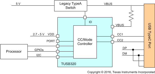 Figure 10. TUSB320 in DRP Mode Supporting Default Implementation
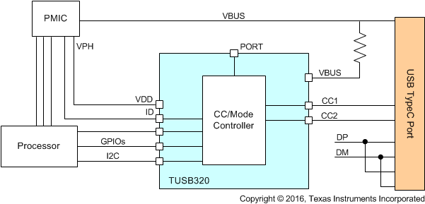 Figure 11. TUSB320 in DRP Mode Supporting Advanced Power Delivery
Figure 12 shows the TUSB320 device configured as a DRP in I2C mode.
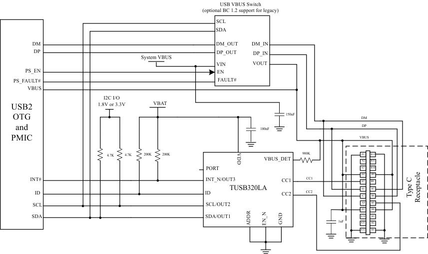 Figure 12. DRP in I2C Mode Schematic
8.2.1.1 Design Requirements
For this design example, use the parameters listed in Table 13:
Table 13. Design Requirements for DRP in I2C Mode
| DESIGN PARAMETER | VALUE |
|---|---|
| VDD (2.75 V to 5 V) | VBAT (less than 5 V) |
| Mode (I2C or GPIO) | I2C: ADDR pin must be pulled down or pulled up |
| I2C address (0x67 or 0x47) | 0x47: ADDR pin must be pulled low or tied to GND |
| Type-C port type (UFP, DFP, or DRP) | DRP: PORT pin is NC |
| Shutdown support | No |
8.2.1.2 Detailed Design Procedure
The TUSB320 device supports a VDD in the range of 2.75 V to 5 V. In this particular use case, VBAT which must be in the required VDD range is connected to the VDD pin. A 100-nF capacitor is placed near VDD.
The TUSB320 device is placed into I2C mode by either pulling the ADDR pin high or low. In this case, the ADDR pin is tied to GND which results in a I2C address of 0x47. The SDA and SCL must be pulled up to either 1.8 V or 3.3 V. When pulled up to 3.3 V, the VDD supply must be at least 3 V to keep from back-driving the I2C interface.
The TUSB320LA device can enter shutdown mode by pulling the EN_N pin high, which puts the TUSB320LA device into a low power state. In this case, external control of the EN_N pin is not implemented and therefore the EN_N pin is tied to GND. The TUSB320HA device can enter shutdown mode by pulling the EN pin low, which puts the TUSB320HA device into a low power state. In this case, external control of the EN pin is not implemented and therefore the EN pin is tied to 1.8 V or 3.3 V.
The INT_N/OUT3 pin is used to notify the PMIC when a change in the TUSB320 I2C registers occurs. This pin is an open drain output and requires an external pullup resistor. The pin should be pulled up to VDD using a 200-kΩ resistor.
The ID pin is used to indicate when a connection has occurred if the TUSB320 device is a DFP while configured for DRP. An OTG USB controller can use this pin to determine when to operate as a USB Host or USB Device. When this pin is driven low, the OTG USB controller functions as a host and then enables VBUS. The Type-C standard requires that a DFP not enable VBUS until the DFP is in the Attached.SRC state. If the ID pin is not low but VBUS is detected, then OTG USB controller functions as a device. The ID pin is open drain output and requires an external pullup resistor. THe ID pin should be pulled up to VDD using a 200-kΩ resistor.
The Type-C port mode is determined by the state of the PORT pin. When the PORT pin is not connected, the TUSB320 device is in DRP mode. The Type-C port mode can also be controlled by the MODE_SELECT register through the I2C interface.
The VBUS_DET pin must be connected through a 900-kΩ resistor to VBUS on the Type-C that is connected. This large resistor is required to protect the TUSB320 device from large VBUS voltage that is possible in present day systems. This resistor along with internal pulldown keeps the voltage observed by the TUSB320 device in the recommended range.
The USB2 specification requires the bulk capacitance on VBUS based on UFP or DFP. When operating the TUSB320 device in a DRP mode, it alternates between UFP and DFP. If the TUSB320 device connects as a UFP, the large bulk capacitance must be removed.
Table 14. USB2 Bulk Capacitance Requirements
| PORT CONFIGURATION | MIN | MAX | UNIT |
|---|---|---|---|
| Downstream facing port (DFP) | 120 | µF | |
| Upstream facing port (UFP) | 1 | 10 | µF |
8.2.1.3 Application Curves
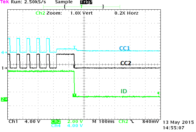 Figure 13. Application Curve for DRP in I2C Mode
8.2.2 DFP in I2C Mode
Figure 14 and Figure 15 show a Type-C configuration for the DFP mode.
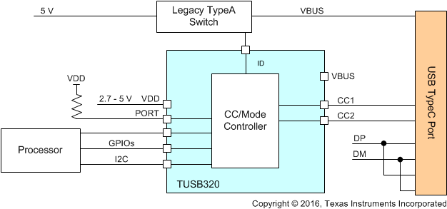 Figure 14. TUSB320 in DFP Mode Supporting Default Implementation
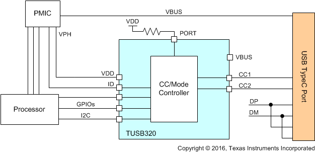 Figure 15. TUSB320 in DFP Mode Supporting Advanced Power Delivery
Figure 16 shows the TUSB320 device configured as a DFP in I2C mode.
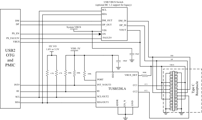 Figure 16. DFP in I2C Mode Schematic
8.2.2.1 Design Requirements
For this design example, use the parameters listed in Table 15:
Table 15. Design Requirements for DFP in I2C Mode
| DESIGN PARAMETER | VALUE |
|---|---|
| VDD (2.75 V to 5 V) | 5 V |
| Mode (I2C or GPIO) | I2C: ADDR pin must be pulled down or pulled up |
| I2C address (0x67 or 0x47) | 0x47: ADDR pin must be pulled low or tied to GND |
| Type-C port type (UFP, DFP, or DRP) | DFP: PORT pin is pulled up |
| Shutdown support | No |
8.2.2.2 Detailed Design Procedure
The TUSB320 device supports a VDD in the range of 2.75 V to 5 V. In this particular case, VDD is set to 5 V. A 100-nF capacitor is placed near VDD.
The TUSB320 device is placed into I2C mode by either pulling the ADDR pin high or low. In this particular case, the ADDR pin is tied to GND which results in a I2C address of 0x47. The SDA and SCL must be pulled up to either 1.8 V or 3.3 V. When pulled up to 3.3 V, the VDD supply must be at least 3 V to keep from back-driving the I2C interface.
The TUSB320LA device can enter shutdown mode by pulling the EN_N pin high, which puts the TUSB320LA device into a low power state. In this case, external control of the EN_N pin is not implemented and therefore the EN_N pin is tied to GND. The TUSB320HA device can enter shutdown mode by pulling the EN pin low, which puts the TUSB320HA device into a low power state. In this case, external control of the EN pin is not implemented and therefore the EN pin is tied to 1.8 V or 3.3 V.
The INT_N/OUT3 pin is used to notify the PMIC when a change in the TUSB320 I2C registers occurs. This pin is an open drain output and requires an external pullup resistor. The pin should be pulled up to VDD using a 200-kΩ resistor.
The Type-C port mode is determined by the state of the PORT pin. When the PORT pin is pulled high, the TUSB320 device is in DFP mode. The Type-C port mode can also be controlled by the MODE_SELECT register through the I2C interface.
The VBUS_DET pin must be connected through a 900-kΩ resistor to VBUS on the Type-C that is connected. This large resistor is required to protect the TUSB320 device from large VBUS voltage that is possible in present day systems. This resistor along with internal pulldown keeps the voltage observed by the TUSB320 device in the recommended range.
The USB2 specification requires the bulk capacitance on VBUS based on UFP or DFP. When operating the TUSB320 device in a DFP mode, a bulk capacitance of at least 120 µF is required. In this particular case, a 150-µF capacitor was chosen.
8.2.2.3 Application Curves
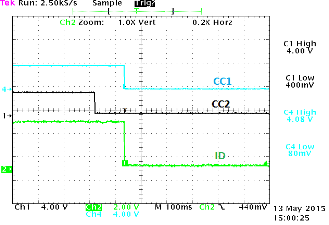 Figure 17. Application Curve for DFP in I2C Mode
8.2.3 UFP in I2C Mode
Figure 18 and Figure 19 show a Type-C configuration for the UFP mode.
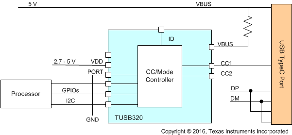 Figure 18. TUSB320 in UFP Mode Supporting Default Implementation
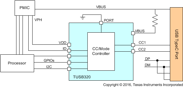 Figure 19. TUSB320 in UFP Mode Supporting Advanced Power Delivery
Figure 20 shows the TUSB320 device configured as a UFP in I2C mode.
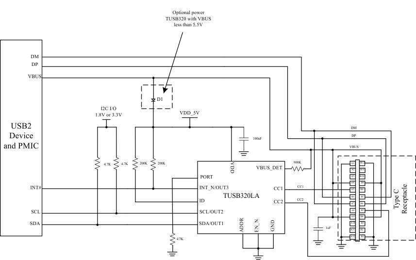 Figure 20. UFP in I2C Mode Schematic
8.2.3.1 Design Requirements
For this design example, use the parameters listed in Table 16:
Table 16. Design Requirements for UFP in I2C Mode
| DESIGN PARAMETER | VALUE |
|---|---|
| VDD (2.75 V to 5 V) | 5 V |
| Mode (I2C or GPIO) | I2C: ADDR pin must be pulled down or pulled up |
| I2C address (0x67 or 0x47) | 0x47: ADDR pin must be pulled low or tied to GND |
| Type-C port type (UFP, DFP, or DRP) | UFP: PORT pin is pulled down |
| Shutdown support | No |
8.2.3.2 Detailed Design Procedure
The TUSB320 device supports a VDD in the range of 2.75 V to 5 V. In this particular case, VDD is set to 5 V. A 100-nF capacitor is placed near VDD. If VBUS is guaranteed to be less than 5.5 V, powering the TUSB320 device through a diode can be implemented.
The TUSB320 device is placed into I2C mode by either pulling the ADDR pin high or low. In this case, the ADDR pin is tied to GND which results in a I2C address of 0x47. The SDA and SCL must be pulled up to either 1.8 V or 3.3 V. When pulled up to 3.3 V, the VDD supply must be at least 3 V to keep from back-driving the I2C interface.
The TUSB320LA device can enter shutdown mode by pulling the EN_N pin high, which puts the TUSB320LA device into a low power state. In this case, external control of the EN_N pin is not implemented and therefore the EN_N pin is tied to GND. The TUSB320HA device can enter shutdown mode by pulling the EN pin low, which puts the TUSB320HA device into a low power state. In this case, external control of the EN pin is not implemented and therefore the EN pin is tied to 1.8 V or 3.3 V.
The INT_N/OUT3 pin is used to notify the PMIC when a change in the TUSB320 I2C registers occurs. This pin is an open drain output and requires an external pullup resistor. The pin should be pulled up to VDD using a 200-kΩ resistor.
The Type-C port mode is determined by the state of the PORT pin. When the PORT pin is pulled low, the TUSB320 device is in UFP mode. The Type-C port mode can also be controlled by the MODE_SELECT register through the I2C interface.
The VBUS_DET pin must be connected through a 900-kΩ resistor to VBUS on the Type-C that is connected. This large resistor is required to protect the TUSB320 device from large VBUS voltage that is possible in present day systems. This resistor along with internal pulldown keeps the voltage observed by the TUSB320 device in the recommended range.
The USB2 specification requires the bulk capacitance on VBUS based on UFP or DFP. When operating the TUSB320 device in a UFP mode, a bulk capacitance between 1 µF to 10 µF is required. In this particular case, a 1-µF capacitor was chosen.
8.2.3.3 Application Curves
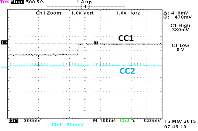 Figure 21. Application Curve for UFP in I2C Mode
8.3 Initialization Setup
8.3.1 TUSB320LA Initialization Procedure
- System is powered off (device has no VDD). The TUSB320LA device is configured internally in UFP mode with Rds on CC pins (dead battery).
- VDD ramps – POR circuit. VDD must ramp within 25 ms or less. IO pull-up power rail (i.e. pull up on ID, INT, SCL, SDA, ADDR, PORT) must ramp with VDD or lag after VDD.
- I2C supply ramps up.
- The TUSB320LA device enters unattached mode and determines the voltage level from the PORT pin. This determines the mode in which the TUSB320LA device operates (DFP, UFP, DRP).
- The TUSB320LA device monitors the CC pins as a DFP and VBUS for attach as a UFP.
- The TUSB320LA device enters active mode when attach has been successfully detected.
8.3.2 TUSB320HA Initialization Procedure
- System is powered off (device has no VDD). The TUSB320HA device is configured internally in UFP mode with Rds on CC pins (dead battery).
- VDD ramps – POR circuit. VDD must ramp within 25 ms or less. IO pull-up power rail (i.e. pull up on ID, INT, SCL, SDA, ADDR, PORT) must ramp with VDD or lag after VDD.
- I2C supply ramps up.
- The TUSB320HA device enters unattached mode and determines the voltage level from the PORT pin. This determines the mode in which the TUSB320HA device operates (DFP, UFP, DRP).
- The TUSB320HA device monitors the CC pins as a DFP and VBUS for attach as a UFP.
- The TUSB320HA device enters active mode when attach has been successfully detected.
9 Power Supply Recommendations
The TUSB320 device has a wide power supply range from 2.7 to 5 V. The TUSB320 device can be run off of a system power such as a battery.
10 Layout
10.1 Layout Guidelines
- An extra trace (or stub) is created when connecting between more than two points. A trace connecting pin A6 to pin B6 will create a stub because the trace also has to go to the USB Host. Ensure that:
- A stub created by short on pin A6 (DP) and pin B6 (DP) at Type-C receptacle does not exceed 3.5 mm.
- A stub created by short on pin A7 (DM) and pin B7 (DM) at Type-C receptacle does not exceed 3.5 mm.
- A 100-nF capacitor should be placed as close as possible to the TUSB320 VDD pin.
10.2 Layout Example
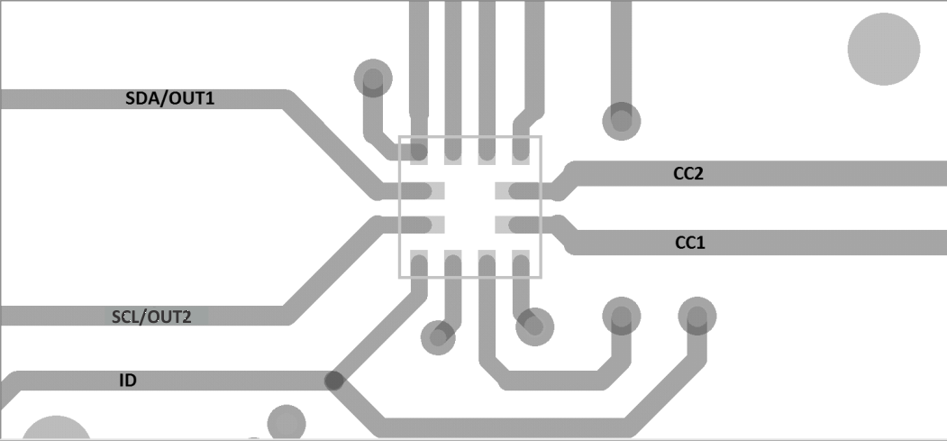 Figure 22. TUSB320 Layout
11 器件和文档支持
11.1 相关链接
下面的表格列出了快速访问链接。类别包括技术文档、支持与社区资源、工具和软件,以及申请样片或购买产品的快速链接。
11.2 接收文档更新通知
要接收文档更新通知,请转至 TI.com 上的器件产品文件夹。单击右上角的通知我 进行注册,即可每周接收产品信息更改摘要。有关更改的详细信息,请查看任何已修订文档中包含的修订历史记录。
11.3 社区资源
下列链接提供到 TI 社区资源的连接。链接的内容由各个分销商“按照原样”提供。这些内容并不构成 TI 技术规范,并且不一定反映 TI 的观点;请参阅 TI 的 《使用条款》。
-
TI E2E™ 在线社区 TI 的工程师对工程师 (E2E) 社区。此社区的创建目的在于促进工程师之间的协作。在 e2e.ti.com 中,您可以咨询问题、分享知识、拓展思路并与同行工程师一道帮助解决问题。
-
设计支持 TI 参考设计支持 可帮助您快速查找有帮助的 E2E 论坛、设计支持工具以及技术支持的联系信息。
11.4 商标
E2E is a trademark of Texas Instruments.
USB Type-C is a trademark of USB Implementers Forum.
All other trademarks are the property of their respective owners.
11.5 静电放电警告

这些装置包含有限的内置 ESD 保护。 存储或装卸时,应将导线一起截短或将装置放置于导电泡棉中,以防止 MOS 门极遭受静电损伤。
11.6 Glossary
SLYZ022 — TI Glossary.
This glossary lists and explains terms, acronyms, and definitions.
12 机械、封装和可订购信息
以下页面包含机械、封装和可订购信息。这些信息是指定器件的最新可用数据。这些数据如有变更,恕不另行通知和修订此文档。如欲获取此产品说明书的浏览器版本,请参阅左侧的导航。
重要声明
德州仪器(TI) 及其下属子公司有权根据 JESD46 最新标准, 对所提供的产品和服务进行更正、修改、增强、改进或其它更改, 并有权根据 JESD48最新标准中止提供任何产品和服务。客户在下订单前应获取最新的相关信息, 并验证这些信息是否完整且是最新的。所有产品的销售都遵循在订单确认时所提供的TI 销售条款与条件。
TI 保证其所销售的组件的性能符合产品销售时 TI 半导体产品销售条件与条款的适用规范。仅在 TI 保证的范围内,且 TI 认为有必要时才会使用测试或其它质量控制技术。除非适用法律做出了硬性规定,否则没有必要对每种组件的所有参数进行测试。
TI 对应用帮助或客户产品设计不承担任何义务。客户应对其使用 TI 组件的产品和应用自行负责。为尽量减小与客户产品和应用相关的风险,客户应提供充分的设计与操作安全措施。
TI 不对任何 TI 专利权、版权、屏蔽作品权或其它与使用了 TI 组件或服务的组合设备、机器或流程相关的 TI 知识产权中授予 的直接或隐含权限作出任何保证或解释。TI所发布的与第三方产品或服务有关的信息,不能构成从 TI 获得使用这些产品或服 务的许可、授权、或认可。使用此类信息可能需要获得第三方的专利权或其它知识产权方面的许可,或是 TI 的专利权或其它知识产权方面的许可。
对于 TI 的产品手册或数据表中 TI 信息的重要部分,仅在没有对内容进行任何篡改且带有相关授权、条件、限制和声明的情况 下才允许进行复制。TI 对此类篡改过的文件不承担任何责任或义务。复制第三方的信息可能需要服从额外的限制条件。
在转售 TI 组件或服务时,如果对该组件或服务参数的陈述与 TI 标明的参数相比存在差异或虚假成分,则会失去相关 TI 组件或服务的所有明示或暗示授权,且这是不正当的、欺诈性商业行为。TI 对任何此类虚假陈述均不承担任何责任或义务。
客户认可并同意,尽管任何应用相关信息或支持仍可能由 TI 提供,但他们将独力负责满足与其产品及在其应用中使用 TI 产品相关的所有法律、法规和安全相关要求。客户声明并同意,他们具备制定与实施安全措施所需的全部专业技术和知识,可预见故障的危险后果、监测故障及其后果、降低有可能造成人身伤害的故障的发生机率并采取适当的补救措施。客户将全额赔偿因 在此类安全关键应用中使用任何 TI 组件而对 TI及其代理造成的任何损失。
在某些场合中,为了推进安全相关应用有可能对 TI 组件进行特别的促销。TI 的目标是利用此类组件帮助客户设计和创立其特有的可满足适用的功能安全性标准和要求的终端产品解决方案。尽管如此,此类组件仍然服从这些条款。
TI 组件未获得用于 FDA Class III(或类似的生命攸关医疗设备)的授权许可,除非各方授权官员已经达成了专门管控此类使 用的特别协议。
只有那些 TI 特别注明属于军用等级或“增强型塑料”的 TI 组件才是设计或专门用于军事/航空应用或环境的。购买者认可并同 意,对并非指定面向军事或航空航天用途的 TI组件进行军事或航空航天方面的应用,其风险由客户单独承担,并且由客户独 力负责满足与此类使用相关的所有法律和法规要求。
TI 已明确指定符合 ISO/TS16949 要求的产品,这些产品主要用于汽车。在任何情况下,因使用非指定产品而无法达到 ISO/TS16949要求,TI不承担任何责任。
产品
- 数字音频: www.ti.com.cn/audio
- 放大器和线性器件: www.ti.com.cn/amplifiers
- 数据转换器: www.ti.com.cn/dataconverters
- DLP® 产品: www.dlp.com
- DSP - 数字信号处理器: www.ti.com.cn/dsp
- 时钟和计时器: www.ti.com.cn/clockandtimers
- 接口: www.ti.com.cn/interface
- 逻辑: www.ti.com.cn/logic
- 电源管理: www.ti.com.cn/power
- 微控制器 (MCU): www.ti.com.cn/microcontrollers
- RFID 系统: www.ti.com.cn/rfidsys
- OMAP应用处理器: www.ti.com/omap
- 无线连通性: www.ti.com.cn/wirelessconnectivity
应用
- 通信与电信: www.ti.com.cn/telecom
- 计算机及周边: www.ti.com.cn/computer
- 消费电子: www.ti.com/consumer-apps
- 能源: www.ti.com/energy
- 工业应用: www.ti.com.cn/industrial
- 医疗电子: www.ti.com.cn/medical
- 安防应用: www.ti.com.cn/security
- 汽车电子: www.ti.com.cn/automotive
- 视频和影像: www.ti.com.cn/video
德州仪器在线技术支持社区: www.deyisupport.com
邮寄地址: 上海市浦东新区世纪大道1568 号,中建大厦32 楼邮政编码: 200122
Copyright© 2016, 德州仪器半导体技术(上海)有限公司