-
TMDS181x 6Gbps TMDS 重定时器
- 1 特性
- 2 应用
- 3 说明
- 4 修订历史记录
- 5 Pin Configuration and Functions
-
6 Specifications
- 6.1 Absolute Maximum Ratings
- 6.2 ESD Ratings
- 6.3 Recommended Operating Conditions
- 6.4 Thermal Information
- 6.5 Power Supply Electrical Characteristics
- 6.6 TMDS Differential Input Electrical Characteristics
- 6.7 TMDS Differential Output Electrical Characteristics
- 6.8 DDC, I2C, HPD, and ARC Electrical Characteristics
- 6.9 Power-Up and Operation Timing Requirements
- 6.10 TMDS Switching Characteristics
- 6.11 HPD Switching Characteristics
- 6.12 DDC and I2C Switching Characteristics
- 6.13 Typical Characteristics
- 7 Parameter Measurement Information
-
8 Detailed Description
- 8.1 Overview
- 8.2 Functional Block Diagram
- 8.3
Feature Description
- 8.3.1 Reset Implementation
- 8.3.2 Operation Timing
- 8.3.3 Swap and Polarity Working
- 8.3.4 TMDS Inputs
- 8.3.5 TMDS Inputs Debug Tools
- 8.3.6 Receiver Equalizer
- 8.3.7 Input Signal Detect Block
- 8.3.8 Audio Return Channel
- 8.3.9 Transmitter Impedance Control
- 8.3.10 TMDS Outputs
- 8.3.11 Pre-Emphasis/De-Emphasis
- 8.4 Device Functional Modes
- 8.5 Register Maps
- 9 Application and Implementation
- 10Power Supply Recommendations
- 11Layout
- 12器件和文档支持
- 13机械、封装和可订购信息
- 重要声明
TMDS181x 6Gbps TMDS 重定时器
1 特性
- HDMI™ 输入端口与输出端口间具有时钟和数据恢复 (CDR) 电路,支持高达 6Gbps 的数据速率
- 在重定时器模式下可兼容高达 6Gbps 的 HDMI™ 电气参数
- 支持 4k2k60p 和高达 WUXGA 16 位色深或 1080p,具有更高的刷新率
- 对输入流重新定时以补偿随机抖动
- 自适应接收器均衡器或可编程固定均衡器
- I2C 和引脚设置可编程
- 5+ 位对内偏移补偿
- 支持单端模式 ARC
- 链路调试工具包括位于RX 均衡器之后眼图
- 48 引脚 7mm × 7mm 0.5mm 间距超薄型四方扁平无引线 (VQFN) 封装
- 扩展商业温度范围为 0°C 至 85°C (TMDS181)
- 工业温度范围为 -40°C 至 85°C (TMDS181I)
2 应用
- 数字电视
- 数字投影仪
- 音频/视频设备
- Blu-Ray™DVD
- 监视器
- 台式机/一体化计算机
- 有源线缆
3 说明
TMDS181x 是一款数字视频接口 (DVI) 或高清多媒体接口 (HDMI™) 重定时器。TMDS181x 支持四条 TMDS 通道,音频返回通道 (SPDIF_IN/ARC_OUT) 和数字显示控制 (DDC) 接口。TMDS181x 支持高达 6Gbps 的信号传输速率,可实现最高分辨率达 4k2k60p 24 位/像素和高达 WUXGA 16 位色深或 1080p,并且具有较高的刷新率。TMDS181x 经配置可支持 HDMI2.0a 标准。TMDS181x 在低于 1.0Gbps 的数据速率下会自动配置为重驱动器,而在高于该速率时会自动配置为重定时器。重驱动器模式支持 HDMI1.4b,数据速率高达 3.4Gbps
TMDS181x 支持双电源轨(VDD 为 1.2V,VCC 为 3.3V),有助于降低功耗。该器件采用多种电源管理方法来降低整体功耗。TMDS181x 通过 I2C 或引脚设置支持固定的接收 EQ 增益或自适应接收 EQ 控制,以补偿不同长度的输入电缆或电路板走线。
器件信息(1)
| 器件型号 | 封装 | 封装尺寸(标称值) |
|---|---|---|
| TMDS181 | VQFN (48) | 7.00mm × 7.00mm |
| TMDS181I |
- 如需了解所有可用封装,请参阅产品说明书末尾的可订购产品附录。
空白
简化电路原理图

4 修订历史记录
Changes from C Revision (July 2016) to D Revision
- Added Note 5 to the Power Supply Electrical Characteristic table Go
- Deleted text "which is needed for certain HDMI CTS test." from the third paragraph in the Overview section Go
- Changed section: Input Signal Detect Block Go
- Changed H to X in the first row of the HPD_SNK column in Table 12Go
- Changed the IN_Dx column in Table 12 Go
Changes from B Revision (April 2016) to C Revision
- Recommended Operating Conditions, Changed the CONTROL PINS section Go
- DDC, I2C, HPD, and ARC Electrical Characteristics, Changed the DDC AND I2C sectionGo
Changes from A Revision (October 2015) to B Revision
- Recommended Operating Conditions, Added VIL "Low-level input voltage at HPD, OE"Go
- Recommended Operating Conditions, Moved pin OE From: VIH MIN value of 2 V To: VIH MIN value of 2.6 V Go
- Power-Up and Operation Timing Requirements, Deleted the VDD_ramp and VCC_ramp MIN values Go
- Changed Figure 1 Go
- DDC Functional Description, Changed text "address 22h (see Figure 31) through the I2C interface." To: "address 0Bh through the I2C interface."Go
- Added Note to 11–400-kbps in Table 6Go
- Added Note to 11–400-kbps in Table 6Go
Changes from * Revision (August 2015) to A Revision
- 已将器件状态从“产品预览”更新为“量产数据”Go
- Absolute Maximum Ratings, Changed max value from 1.56 V to VCC + 0.3V; added input current and Min valueGo
- Absolute Maximum Ratings, Added Max Input Current on Main Link Differential Input pinsGo
- Recommended Operating Conditions, Updated the note showing the values shown are only for Microcontroller driven and not values based upon pull up or pull down resistors. Go
- Power Supply Electrical Characteristics, Increased Max Value of ISD2 from 10 to 15mA Go
- TMDS Differential Input Electrical Characteristics, Changed Max Receiver impedance value to 115 Go
- DDC, I2C, HPD, and ARC Electrical Characteristics, Inserted values for SCL/SDA_SNK Go
- TMDS Switching Characteristics, Changed from 6000 to 3400 Go
- Table 4, Deleted Clear and NA Access Tags Go
- Table 8, Removed reg20h[5:4] ARC_SWING Go
- Figure 35, Removed 1k pullup from switch as not needed Go
- Pin Strapping Configuration for HDMI2.0a and HDMI1.4b, Added Note for VSADJ resistor value in Compliance Pin Strapping section Go
- Pin Strapping Configuration for HDMI2.0a and HDMI1.4b, Changed De-emphasis value from 0 dB to -2 dB for recommended configuration for compliance testing.Go
- I2C Control for HDMI2.0a and HDMI1.4b, Added Note for VSADJ resistor value in Compliance I2C control section and included register that can increase or decrease the VOD swing Go
5 Pin Configuration and Functions

Pin Functions(2)
| PIN | TYPE(1) | DESCRIPTION | |
|---|---|---|---|
| NAME | NO. | ||
| VCC | 13, 43 | P | 3.3 V power supply |
| VDD | 14, 23, 24, 37, 48 | P | 1.2 V power supply |
| GND | 7, 19, 41, 30, Thermal pad |
G | Ground |
| MAIN LINK INPUT PINS | |||
| IN_D2p/n | 2, 3 | I | Channel 2 differential input |
| IN_D1p/n | 5, 6 | I | Channel 1 differential input |
| IN_D0p/n | 8, 9 | I | Channel 0 differential input |
| IN_CLKp/n | 11, 12 | I | Clock differential input |
| MAIN LINK OUTPUT PINS (FAIL SAFE) | |||
| OUT_D2n/p | 34, 35 | O | TMDS data 2 differential output |
| OUT_D1n/p | 31, 32 | O | TMDS data 1 differential output |
| OUT_D0n/p | 28, 29 | O | TMDS data 0 differential output |
| OUT_CLKn/p | 25, 26 | O | TMDS data clock differential output |
| HOT PLUG DETECT PINS | |||
| HPD_SRC | 4 | O | Hot plug detect output to source side |
| HPD_SNK | 33 | I | Hot plug detect input from sink side |
| AUDIO RETURN CHANNEL AND DDC PINS | |||
| SPDIF_IN ARC_OUT |
45 44 |
I/O | SPDIF signal input Audio return channel output |
| SDA_SRC SCL_SRC |
47 46 |
I/O | Source side TMDS port bidirectional DDC data line Source side TMDS port bidirectional DDC clock line |
| SDA_SNK SCL_SNK |
39 38 |
I/O | Sink side TMDS port bidirectional DDC data line Sink side TMDS port bidirectional DDC clock line |
| CONTROL PINS | |||
| OE | 42 | I | Operation enable/reset pin OE = L: Power-down mode OE = H: Normal operation Internal weak pull up: Resets device when transitions from H to L |
| SIG_EN | 17 | I | Signal detector circuit enable SIG_EN = L: Signal detect circuit disabled: SIG_EN = H: Signal detect circuit enabled: When no valid clock device enters standby mode. Internal weak pull down |
| PRE_SEL | 20 | I 3 level |
De-emphasis control when I2C_EN/PIN = Low. PRE_SEL = L: –2 dB PRE_SEL = No Connect: 0 dB PRE_SEL = H: Reserved When I2C_EN/PIN = High de-emphasis is controlled through I2C |
| EQ_SEL/A0 | 21 | I 3 level |
Input receive equalization pin strap when I2C_EN/PIN = Low EQ_SEL = L: Fixed EQ at 7.5 dB at 3 GHz EQ_SEL = No Connect: Adaptive EQ EQ_SEL = H: Fixed at 14 dB at 3 GHz When I2C_EN/PIN = High address bit 1 Note: 3 level for pin strap programming but 2 level when I2C address |
| I2C_EN/PIN | 10 | I | I2C_EN/PIN = High; puts device into I2C Control Mode I2C_EN/PIN = Low; puts device into pin strap mode Note: I2C CSR is addressable at all times, but features that can be controlled by pin strapping can only be changed by I2C when this pin is pulled high |
| SCL_CTL | 15 | I | I2C clock signal Note: When I2C_EN = Low Pin strapping takes priority and those functions cannot be changed by I2C |
| SDA_CTL | 16 | I/0 | I2C data signal Note: When I2C_EN = Low Pin strapping takes priority and those functions cannot be changed by I2C |
| VSadj | 22 | I | TMDS-compliant voltage swing control nominal resistor to GND |
| A1 | 27 | I | High address bit 2 for I2C programming Weak internal pull down Note: When in Pin Strapping Mode leave pin as No connect |
| TX_TERM_CTL | 36 | I 3 level |
Transmit termination control TX_TERM_CTL = H, no transmit termination TX_TERM_CTL = L, transmit termination impedance in approximately 75 to 150 Ω TX_TERM_CTL = No Connect, automatically selects the termination impedance Data rate (DR) > 3.4 Gbps – 75 to 150 Ω differential near end termination 2 Gbps > DR < 3.4 Gbps – 150 to 300 Ω differential near end termination DR < 2 Gbps – no termination Note: If left floating will be in automatic select mode. |
| SWAP/POL | 1 | I 3 level |
Input lane SWAP and polarity control pin SWAP/POL = H: receive lanes polarity swap (retimer mode only) SWAP/POL = L: receive lanes swap (redriver and retimer mode) SWAP/POL = No Connect: normal operation |
| NC | 18, 40 | NA | No connect |
6 Specifications
6.1 Absolute Maximum Ratings
over operating free-air temperature range (unless otherwise noted) (1)(2)| MIN | MAX | UNIT | ||
|---|---|---|---|---|
| Supply voltage(3) | VCC | –0.3 | 4 | V |
| VDD | –0.3 | 1.4 | ||
| Voltage | Main link input differential voltage (IN_Dx, IN_CLKx) IIN = 15mA | VCC - 0.75V | VCC + 0.3V | V |
| TMDS outputs ( OUT_Dx) | –0.3 | 4 | ||
| HPD_SRC, Vsadj, SDA_CTL, SCL_CTL, OE, A1, PRE_SEL, EQ_SEL/A0, I2C_EN/PIN, SIG_EN, TX_TERM_CTL, | –0.3 | 4 | ||
| HDP_SNK, SDA_SNK, SCL_SNK, SDA_SRC, SCL_SRC | –0.3 | 6 | ||
| Input Current IIN | Main link input current (IN_Dx, IN_CLKx) | 15 | mA | |
| Continuous power dissipation | See Thermal Information | |||
| Tstg | Storage temperature | –65 | 150 | °C |
6.2 ESD Ratings
| VALUE | UNIT | |||
|---|---|---|---|---|
| V(ESD) | Electrostatic discharge | Human-body model (HBM), per ANSI/ESDA/JEDEC JS-001(1) | ±2000 | V |
| Charged-device model (CDM), per JEDEC specification JESD22-C101(2) | ±500 | |||
6.3 Recommended Operating Conditions
over operating free-air temperature range (unless otherwise noted)| MIN | NOM | MAX | UNIT | |||
|---|---|---|---|---|---|---|
| VCC | Supply voltage nominal value 3.3 V | 3.135 | 3.3 | 3.465 | V | |
| VDD | Supply voltage nominal value 1.2 V | 1.1 | 1.2 | 1.27 | V | |
| TCASE | Case temperature | 92.7 | °C | |||
| TA | Operating free-air temperature | TMDS181 | 0 | 85 | °C | |
| TMDS181I | –40 | 85 | °C | |||
| MAIN LINK DIFFERENTIAL PINS | ||||||
| VID_PP | Peak-to-peak input differential voltage | 75 | 1560 | mVpp | ||
| VIC | Input common mode voltage | VCC – 0.4 | VCC + 0.1 | V | ||
| dR | Data rate | 0.25 | 6 | Gbps | ||
| RVSADJ | TMDS compliant swing voltage bias resistor nominal | 4.5 | 7.06 | kΩ | ||
| CONTROL PINS | ||||||
| VI-DC | DC input voltage | Control pins | –0.3 | 3.6 | V | |
| VIL(1) | Low-level input voltage at PRE_SEL, EQ_SEL/A0, TX_TERM_CTL, SWAP/POL pins only | 0.3 | V | |||
| Low-level input voltage at OE | 0.8 | |||||
| VIM(1) | Mid-level input voltage at PRE_SEL, EQ_SEL/A0, TX_TERM_CTL, SWAP/POL pins only | 1 | 1.2 | 1.4 | V | |
| VIH(1) | High-level input voltage at PRE_SEL, EQ_SEL/A0, TX_TERM_CTL, SWAP/POL, OE(2) pins only | 2.6 | V | |||
| VOL | Low-level output voltage | 0.4 | V | |||
| VOH | High-level output voltage | 2.4 | V | |||
| IIH | High-level input current | –30 | 30 | µA | ||
| IIL | Low-level input current | –25 | 25 | µA | ||
| IOS | Short-circuit output current | –50 | 50 | mA | ||
| IOZ | High impedance output current | 10 | µA | |||
| ROEPU | Pullup resistance on OE pin | 150 | 250 | kΩ | ||
6.4 Thermal Information
| THERMAL METRIC(1)(2) | TMDS181x | UNIT | |
|---|---|---|---|
| RGZ (VQFN) | |||
| 48 PINS | |||
| RθJA | Junction-to-ambient thermal resistance | 31.1 | °C/W |
| RθJC(top) | Junction-to-case (top) thermal resistance | 18.2 | °C/W |
| RθJB | Junction-to-board thermal resistance | 8.1 | °C/W |
| ψJT | Junction-to-top characterization parameter | 0.4 | °C/W |
| ψJB | Junction-to-board characterization parameter | 8.1 | °C/W |
| RθJC(bot) | Junction-to-case (bottom) thermal resistance | 3.2 | °C/W |
6.5 Power Supply Electrical Characteristics
over operating free-air temperature range (unless otherwise noted)| PARAMETER | TEST CONDITIONS | MIN | TYP(2) | MAX(1) | UNIT | ||
|---|---|---|---|---|---|---|---|
| PD1(3)(4) | Device power dissipation (retimer operation) |
OE = H, VCC = 3.3 V/3.465 V, VDD = 1.2 V/1.27 V IN_Dx: VID_PP = 1200 mV, 6 Gbps TMDS pattern, VI = 3.3 V, I2C_EN/PIN = L, PRE_SEL= NC, EQ_SEL= NC, SDA_CTL/CLK_CTL = 0 V |
800 | 900 | mW | ||
| PD2(3)(4) | Device power dissipation (redriver operation) |
OE = H, VCC = 3.3 V/3.465 V, VDD = 1.2 V/1.27 V IN_Dx: VID_PP = 1200 mV, 2.97 Gbps TMDS pattern, VI = 3.3 V, I2C_EN/PIN = L, PRE_SEL= NC, EQ_SEL= H, SDA_CTL/CLK_CTL = 0 V |
500 | 600 | mW | ||
| PSD1(3)(4)(5) | Device power in standby | OE = H, VCC = 3.3 V/3.465 V, VDD = 1.2 V/1.27 V, HPD = H, No valid input signal | 50 | 100 | mW | ||
| PSD2(3)(4)(5) | Device power in power down | OE = L, VCC = 3.3 V/3.465 V, VDD = 1.2 V/1.27 V | 10 | 30 | mW | ||
| ICC1(3)(4) | VCC supply current (TMDS 6Gpbs retimer mode) | OE = H, VCC = 3.3 V/3.465 V, VDD = 1.2 V/1.27 V IN_Dx: VID_PP = 1200 mV, 6 Gbps TMDS pattern I2C_EN/PIN = L, PRE_SEL = NC, EQ_CTL = NC, SDA_CTL/CLK_CTL = 0 V |
131 | 150 | mA | ||
| IDD1(3)(4) | VDD supply current (TMDS 6Gpbs retimer mode) | OE = H, VCC = 3.3 V/3.465 V, VDD = 1.2 V/1.27 V IN_Dx: VID_PP = 1200 mV, 6 Gbps TMDS pattern I2C_EN/PIN = L, PRE_SEL = NC, EQ_CTL = NC, SDA_CTL/CLK_CTL = 0 V |
332 | 350 | mA | ||
| ICC2(3)(4) | VCC supply current (TMDS 6Gpbs redriver mode) | OE = H, VCC = 3.3 V/3.465 V, VDD = 1.2 V/1.27 V IN_Dx: VID_PP = 1200 mV, 2.97 Gbps TMDS pattern I2C_EN/PIN = L, PRE_SEL = NC, EQ_CTL = H, SDA_CTL/CLK_CTL = 0 V |
92 | mA | |||
| IDD2(3)(4) | VDD supply current (TMDS 6Gpbs redriver mode) | OE = H, VCC= 3.3 V/3.465 V, VDD = 1.2 V/1.27 V IN_Dx: VID_PP = 1200 mV, 3.4 Gbps TMDS pattern I2C_EN/PIN = L, PRE_SEL = NC, EQ_CTL = H, SDA_CTL/CLK_CTL = 0 V |
187 | mA | |||
| ISD1(5) | Standby current | OE = H, VCC = 3.3 V/3.465 V, VDD = 1.2 V/1.27 V, HPD = H: No valid signal on IN_CLK | 3.3 V rail(3) | 6 | 15 | mA | |
| 1.2 V rail | 40 | 50 | |||||
| ISD2(5) | Power-down current | OE = L, VCC = 3.3 V/3.465 V, VDD = 1.2 V/1.27 V | 3.3 V rail(3) | 2 | 5 | mA | |
| 1.2 V rail | 3.5 | 15 | |||||
6.6 TMDS Differential Input Electrical Characteristics
over operating free-air temperature range (unless otherwise noted)| PARAMETER | TEST CONDITIONS | MIN | TYP(2) | MAX(1) | UNIT | |
|---|---|---|---|---|---|---|
| DR_RX_DATA_RT | TMDS data lanes data rate (Retimer Mode) | 0.25 | 6 | Gbps | ||
| DR_RX_DATA_RD | TMDS data lanes data rate (Redriver Mode) | 0.25 | 3.4 | Gbps | ||
| DR_RX_CLK | TMDS clock lanes clock rate | 25 | 340 | MHz | ||
| tRX_DUTY | Input clock duty circle | 40% | 50% | 60% | ||
| tCLK_JIT | Input clock jitter tolerance | 0.3 | Tbit | |||
| tDATA_JIT | Input data jitter tolerance | Test the TTP2, see Figure 12 | 150 | ps | ||
| tRX_INTRA | Input intrapair skew tolerance | Test at TTP2 when DR = 1.6 Gbps, see Figure 12 | 112 | ps | ||
| tRX_INTER | Input interpair skew tolerance | 1.8 | ns | |||
| EQH(D) | Fixed EQ gain for data lane IN_D(0,1,2)n/p | EQ_SEL/A0 = H; fixed EQ gain, test at 6 Gbps | 15 | dB | ||
| EQL(D) | Fixed EQ gain for data lane IN_D(0,1,2)n/p | EQ_SEL/A0 = L; fixed EQ gain, test at 6 Gbps | 7.5 | dB | ||
| EQZ(D) | Adaptive EQ gain for data lane IN_D(0,1,2)n/p | EQ_SEL/A0 = NC; adaptive EQ (Retimer Mode Only) | 2 | 15 | dB | |
| EQ(c) | EQ gain for clock lane IN_CLKn/p | EQ_SEL/A0 = H,L,NC | 3 | dB | ||
| RINT | Input differential termination impedance | 85 | 100 | 115 | Ω | |
| VITERM | Input termination voltage | OE = H | 3.3 | 3.465 | V | |
6.7 TMDS Differential Output Electrical Characteristics
over operating free-air temperature range (unless otherwise noted)| PARAMETER | TEST CONDITIONS | MIN | TYP(2) | MAX(1) | UNIT | |
|---|---|---|---|---|---|---|
| VOH | Single-ended high level output voltage Data rate ≤1.65 Gbps |
PRE_SEL = NC; TX_TERM_CTL = H; OE = H; DR = 750 Mbps; VSadj = 7.06 kΩ; | VCC – 10 | VCC + 10 | V | |
| Single-ended high level output voltage Data rate >1.65 Gbps and <3.4 Gbps |
PRE_SEL = NC; TX_TERM_CTL = NC; OE = H; DR = 2.97 Gbps; VSadj = 7.06 kΩ; | VCC-200 | VCC + 10 | |||
| Single-ended high level output voltage Data rate >3.4 Gbps and < 6 Gbps(1) |
PRE_SEL = NC; TX_TERM_CTL = L; OE = H; DR = 6 Gbps; VSadj = 7.06 kΩ; | VCC – 400 | VCC + 10 | |||
| VOL | Single-ended low level output voltage Data rate ≤1.65 Gbps |
PRE_SEL = NC; TX_TERM_CTL = H; OE = H; DR = 750 Mbps; VSadj = 7.06 kΩ; | VCC – 600 | VCC – 400 | V | |
| Single-ended low level output voltage Data rate >1.65 Gbps and <3.4 Gbps |
PRE_SEL = NC; TX_TERM_CTL = NC; OE = H; DR = 2.97 Gbps; VSadj = 7.06 kΩ; | VCC – 700 | VCC – 400 | |||
| Single-ended low level output voltage Data rate >3.4 Gbps and < 6 Gbps(1) |
PRE_SEL = NC; TX_TERM_CTL = L; OE = H; DR = 6 Gbps; VSadj = 7.06 kΩ; | VCC – 1000 | VCC – 400 | |||
| VSWING_DA | Single-ended output voltage swing on data lane | PRE_SEL = NC; TX_TERM_CTL = H/NC/L; OE = H; DR = 270 Mbps/2.97/6 Gbps VSadj = 7.06 kΩ; | 400 | 500 | 600 | mV |
| VSWING_CLK | Single-ended output voltage swing on clock lane | PRE_SEL = NC; TX_TERM_CTL = H; OE = H; Data rate ≤ 3.4 Gbps; VSadj = 7.06 kΩ; | 400 | 500 | 600 | mV |
| PRE_SEL = NC; TX_TERM_CTL = NC; OE = H; Data rate > 3.4 Gbps; VSadj = 7.06 kΩ; | 200 | 300 | 400 | |||
| ΔVSWING | Change in single-end output voltage swing per 100 Ω ΔVSadj | 20 | mV | |||
| ΔVOCM(SS) | Change in steady state output common mode voltage between logic levels | –5 | 5 | mV | ||
| VOD(PP) | Output differential voltage before pre-emphasis | VSADJ = 7.06 kΩ; PRE_SEL = NC see Figure 10 | 800 | 1200 | mV | |
| VOD(SS) | Steady state output differential voltage | VSADJ = 7.06 kΩ; PRE_SEL = L, see Figure 11 | 600 | 1075 | mV | |
| VOD_range | Total TMDS data lanes output differential voltage for HDMI2.0. Retimer Mode Only See Figure 14 |
3.4 Gbps < Rbit ≤ 3.712 Gps TX_TERM_CTL = NC; PRE_SEL = NC; OE = H; VSadj = 7.06 kΩ; |
335 | mV | ||
| 3.712 Gbps < Rbit < 5.94 Gbps TX_TERM_CTL = NC; PRE_SEL = NC; OE = H; VSadj = 7.06 kΩ; |
–19.66 × (Rbit2) + (106.74 × Rbit) + 209.58 | |||||
| 5.94 Gbps ≤ Rbit ≤ 6.0 Gbps TX_TERM_CTL = NC; PRE_SEL = NC; OE = H; VSadj = 7.06 kΩ; |
150 | |||||
| IOS | Short-circuit current limit | Main link output shorted to GND | 50 | mA | ||
| ILEAK | Failsafe condition leakage current | VCC = 0 V; VDD = 0 V; TMDS Outputs pulled to 3.3 V through 50 Ω resistor; | 45 | μA | ||
| RTERM | Source termination resistance for HDMI2.0 | 75 | 150 | Ω | ||
6.8 DDC, I2C, HPD, and ARC Electrical Characteristics
over operating free-air temperature range (unless otherwise noted)| PARAMETER | TEST CONDITIONS | MIN | TYP(2) | MAX(1) | UNIT | |
|---|---|---|---|---|---|---|
| DDC AND I2C | ||||||
| VI-DC | SCL/SDA_SNK, SCL/SDA_SRC DC input voltage | –0.3 | 5.5 | V | ||
| SCL/SDA_CTL, DC input voltage | –0.3 | 3.6 | V | |||
| VIL | SCL/SDA_SNK, SCL/SDA_SRC Low level input voltage | 0.3 x VCC | V | |||
| SCL/SDA_CTL Low level input voltage | 0.3 x VCC | V | ||||
| VIH | SCL/SDA_SNK, SCL/SDA_SRC high level input voltage | 3 | V | |||
| SCL/SDA_CTL high level input voltage | 0.7 x VCC | V | ||||
| VOL | SCL/SDA_CTL, SCL/SDA_SRC low level output voltage | I0 = 3 mA and VCC > 2 V | 0.4 | V | ||
| I0 = 3 mA and VCC < 2 V | 0.2 x VCC | |||||
| fSCL | SCL clock frequency fast I2C mode for local I2C control | 400 | kHz | |||
| Cbus | Total capacitive load for each bus line (DDC and local I2C pins) | 400 | pF | |||
| HPD | ||||||
| VIH | High-level input voltage | HPD_SNK | 2.1 | V | ||
| VIL | Low-level input voltage | HPD_SNK | 0.8 | V | ||
| VOH | High-level output voltage | IOH = –500 µA; HPD_SRC, | 2.4 | 3.6 | V | |
| VOL | Low-level output voltage | IOL = 500 µA; HPD_SRC, | 0 | 0.1 | V | |
| ILEAK | Failsafe condition leakage current | VCC = 0 V; VDD = 0 V; HPD_SNK = 5 V; | 40 | μA | ||
| IH_HPD | High-level input current | Device powered; VIH = 5 V; IH_HPD includes RpdHPD resistor current |
40 | µA | ||
| Device powered; VIL = 0.8 V; IL_HPD includes RpdHPD resistor current |
30 | |||||
| RpdHPD | HPD input termination to GND | VCC = 0 V | 150 | 190 | 220 | kΩ |
| SPDIF AND ARC | ||||||
| VEL | Operating DC voltage for single mode ARC output | Test at ARC_OUT, see Figure 22 | 0 | 5 | V | |
| VIN_DC | Operating DC voltage for SPDIF input | 0.05 | V | |||
| VSP_SW | Signal amplitude of SPDIF input | 0.2 | 0.5 | 0.6 | V | |
| VElSWING | Signal amplitude on the ARC output | Test at ARC_OUT, 55 Ω external termination resistor, see Figure 22 | 0.4 | 0.5 | 0.6 | V |
| CLK_ARC | Signal frequency on ARC | Test at ARC_OUT, see Figure 22 | 3.687 | 5.645 ±0.1% | 13.517 | MHz |
| Duty cycle | Output clock duty cycle | 45% | 50% | 55% | ||
| Data rate | SPDIF input DR | 7.373 | 11.29 | 27.034 | Mbps | |
| tEDGE | Rise/fall time for ARC output | From 10% to 90% voltage level | 0.4 | UI | ||
| R_IN_SPDIF | Input termination resistance for SPDIF | 75 | Ω | |||
| Rest | Single mode output termination resistance | 0.1 MHz to 128× the maximum frame rate | 36 | 55 | 75 | Ω |
6.9 Power-Up and Operation Timing Requirements
over operating free-air temperature range (unless otherwise noted) (1) Figure 2. CDR Timing for TMDS181
6.10 TMDS Switching Characteristics
over operating free-air temperature range (unless otherwise noted)| PARAMETER | TEST CONDITIONS | MIN | TYP(2) | MAX(1) | UNIT | |
|---|---|---|---|---|---|---|
| REDRIVER MODE | ||||||
| dR | Data rate (redriver mode) | 250 | 3400 | Mbps | ||
| tPLH | Propagation delay time (low to high) | 250 | 600 | ps | ||
| tPHL | Propagation delay time (high to low) | 250 | 800 | ps | ||
| tT1(1.4b) | Transition time (rise and fall time); measured at 20% and 80% levels for data lanes. TMDS clock meets tT3 for all three times. | TX_TERM_CTL = NC; PRE_SEL = NC; OE = H; 1.48 Gbps and 2.97 Gbps data lines, 148 MHz and 297 MHz clock | 75 | ps | ||
| tT3 | TX_TERM_CTL = NC; PRE_SEL = NC; OE = H; 1.48 Gbps, 2.97 Gbps | 100 | ps | |||
| tSK_INTRA | Intra-pair output skew | Default setting for internal intra-pair skew adjust, TX_TERM_CTL = NC; PRE_SEL = NC; 1.48 Gbps, 2.97 Gbps; See Figure 8 | 40 | ps | ||
| tSK_INTER | Inter-pair output skew | Default setting for internal inter-pair skew adjust, TX_TERM_CTL = NC; PRE_SEL = NC; 1.48 Gbps, 2.97 Gbps; See Figure 8 | 100 | ps | ||
| tJITD1(1.4b) | Total output data jitter HDMI1.4b | DR = 2.97 Gbps, PRE_SEL = NC, EQ_SEL/A0 = NC ; . See Figure 12 at TTP3 | 0.2 | Tbit | ||
| tJITC1(1.4b) | Total output clock jitter | CLK = 25 MHz, 74.25 MHz, 75 MHz, 150 MHz, 297 MHz | 0.25 | Tbit | ||
| RETIMER MODE | ||||||
| dR | Data rate (retimer mode) | 0.25 | 6 | Gbps | ||
| dXVR | Automatic redriver to retimer crossover (when selected) | Measured with input signal applied = 200 mVpp | 0.75 | 1 | 1.25 | Gbps |
| fCROSSOVER | Crossover frequency hysteresis | 250 | MHz | |||
| PLLBW | Data retimer PLL bandwidth | Default loop bandwidth setting | 0.4 | 1 | MHz | |
| tACQ | Input clock frequency detection and retimer acquisition time | 180 | µs | |||
| IJT1 | Input clock jitter tolerance | Tested when data rate >1.0Gbps | 0.3 | Tbit | ||
| tT1(2.0) | Transition time (rise and fall time); measured at 20% and 80% levels for data lanes. TMDS clock meets tT3 for all three times. | TX_TERM_CTL = L; PRE_SEL = NC; 6 Gbps data lines, | 45 | ps | ||
| tT1 (1.4b) | TX_TERM_CTL = NC; PRE_SEL = NC; 1.48 Gbps and 2.97 Gbps data lines, 148 MHz and 297 MHz clock | 75 | ps | |||
| tT3 | TX_TERM_CTL = NC; PRE_SEL = NC; 1.48 Gbps, 2.97 Gbps, 6 Gbps data lines, 148 MHz, 297 MHz clock | 100 | ps | |||
| tDCD | OUT_CLK ± duty cycle | 40% | 50% | 60% | ||
| tSK_INTER | Inter-pair output skew | Default setting for internal inter-pair skew adjust, TX_TERM_CTL = NC; PRE_SEL = NC; 1.48 Gbps, 2.97 Gbps, 6 Gbps data lines, 148 MHz, 297 MHz clock; See Figure 8 | 0.2 | Tch | ||
| tSK_INTRA | Intra-pair output skew | Default setting for internal intra-pair skew adjust, TX_TERM_CTL = NC; PRE_SEL = NC; 1.48 Gbps, 2.97 Gbps, 6 Gbps data lines, 148 MHz, 297 MHz clock; See Figure 8 | 0.15 | Tbit | ||
| tJITC1(1.4b) | Total output clock jitter | CLK = 25 MHz, 74.25 MHz, 75 MHz, 150 MHz, 297 MHz | 0.25 | Tbit | ||
| tJITC1(2.0) | DR = 6 Gbps: CLK = 150 MHz | 0.3 | Tbit | |||
| tJITD2 | Total output data jitter See Figure 14 |
3.4 Gbps < Rbit ≤ 3.712 Gps TX_TERM_CTL = NC; PRE_SEL = NC; OE = H |
0.4 | Tbit | ||
| 3.712 Gbps < Rbit < 5.94 Gbps TX_TERM_CTL = NC; PRE_SEL = NC; OE = H |
–0.0332Rbit2 + 0.2312Rbit + 0.1998 | |||||
| 5.94 Gbps ≤ Rbit ≤ 6.0 Gbps TX_TERM_CTL = NC; PRE_SEL = NC; OE = H |
0.6 | |||||
6.11 HPD Switching Characteristics
over operating free-air temperature range (unless otherwise noted)| PARAMETER | TEST CONDITIONS | MIN | TYP(2) | MAX(1) | UNIT | |
|---|---|---|---|---|---|---|
| tPD(HPD) | Propagation delay from HPD_SNK to HPD_SRC; rising edge and falling edge(1) | See Figure 16; not valid during switching time | 40 | 120 | ns | |
| tT(HPD) | HPD logical disconnected timeout | See Figure 17 | 2 | ms | ||
6.12 DDC and I2C Switching Characteristics
over operating free-air temperature range (unless otherwise noted) (1)| PARAMETER | TEST CONDITIONS | MIN | TYP | MAX | UNIT | |
|---|---|---|---|---|---|---|
| tr | Rise time of both SDA and SCL signals | VCC = 3.3 V | 300 | ns | ||
| tf | Fall time of both SDA and SCL signals | 300 | ns | |||
| tHIGH | Pulse duration, SCL high | 0.6 | μs | |||
| tLOW | Pulse duration, SCL low | 1.3 | μs | |||
| tSU1 | Setup time, SDA to SCL | 100 | ns | |||
| tST, STA | Setup time, SCL to start condition | 0.6 | μs | |||
| tHD,STA | Hold time, start condition to SCL | 0.6 | μs | |||
| tST,STO | Setup time, SCL to stop condition | 0.6 | μs | |||
| t(BUF) | Bus free time between stop and start condition | 1.3 | μs | |||
| tPLH1 | Propagation delay time, low-to-high-level output | Source to sink: 100kbps pattern; Cb(Sink) = 400 pF(1); see Figure 20 | 360 | ns | ||
| tPHL1 | Propagation delay time, high-to-low-level output | 230 | ns | |||
| tPLH2 | Propagation delay time, low-to-high-level output | Sink to source: 100kbps pattern; Cb(Source) = 100 pF(1); see Figure 21 | 250 | ns | ||
| tPHL2 | Propagation delay time, high-to-low-level output | 200 | ns | |||
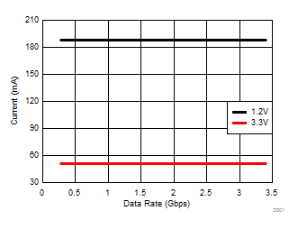
6.13 Typical Characteristics
7 Parameter Measurement Information
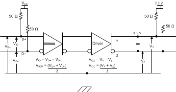 Figure 6. TMDS Main Link Test Circuit
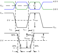 Figure 7. Input/Output Timing Measurements
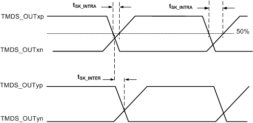 Figure 8. TMDS Output Skew Measurements
 Figure 9. HDMI/DVI TMDS Output Common Mode Measurement
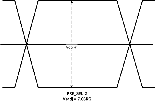 Figure 10. Output Differential Waveform
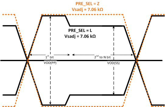 Figure 11. Output De-Emphasis Waveform
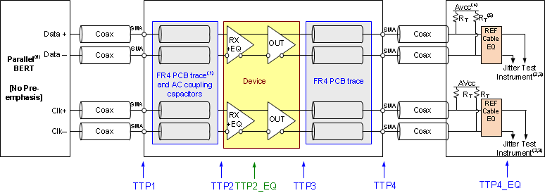
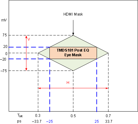 Figure 13. Input Eye Mask Post EQ – TTP2_EQ
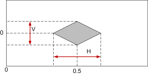
Table 1. Output Eye Mask V and H Values
| TMDS Data Rate (Gbps) | H (Tbit) | V (mV) |
|---|---|---|
| 3.4 < DR < 3.712 | 0.6 | 335 |
| 3.712 < DR < 5.94 | –0.0332Rbit2 +0.2312 Rbit + 0.1998 | –19.66Rbit2 + 106.74Rbit + 209.58 |
| 5.94 ≤ DR ≤ 6.0 | 0.4 | 150 |
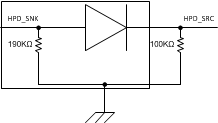 Figure 15. HPD Test Circuit
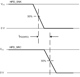 Figure 16. HPD Timing Diagram 1
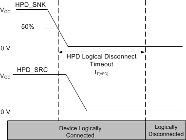 Figure 17. HPD Logic Disconnect Timeout
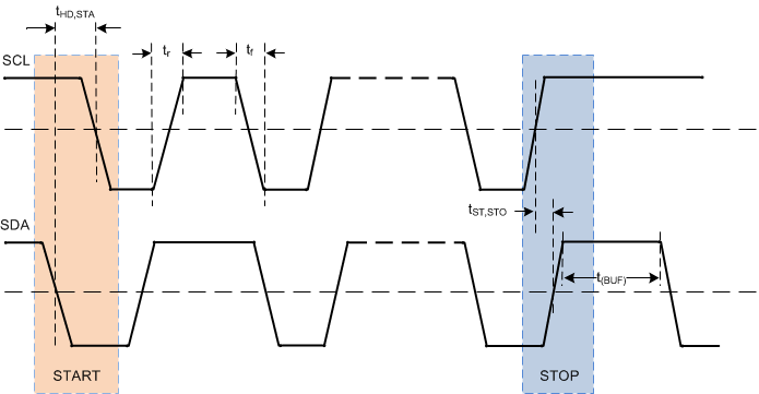 Figure 18. START and STOP Condition Timing
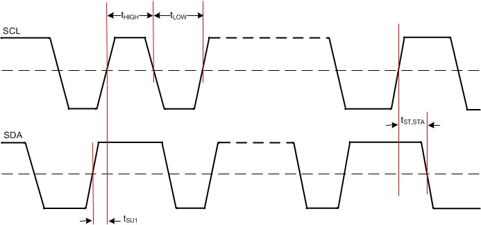 Figure 19. SCL and SDA Timing
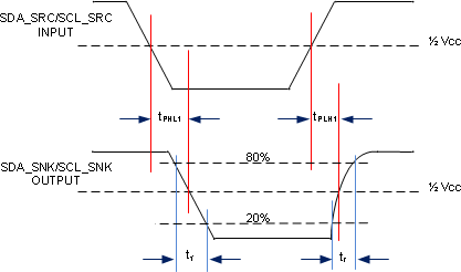 Figure 20. DDC Propagation Delay – Source to Sink
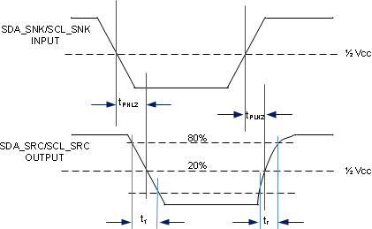 Figure 21. DDC Propagation Delay – Sink to Source
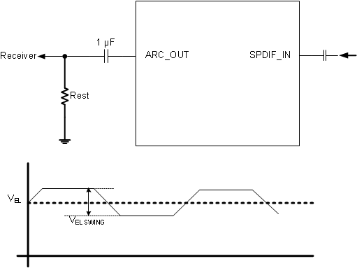 Figure 22. ARC Output
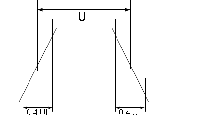 Figure 23. Rise and Fall Time of ARC
8 Detailed Description
8.1 Overview
The TMDS181 is a DVI or HDMI™ retimer. The TMDS181 supports four TMDS channels, audio return channel (SPDIF_IN/ARC_OUT), hot plug detect, and DDC interfaces. The TMDS181 supports signaling rates up to 6 Gbps in retimer mode to allow for the highest resolutions of 4k2k60p 24 bits per pixel and up to WUXGA 16-bit color depth or 1080p with higher refresh rates. In redriver mode it supports HDMI1.4b with data rates up to 3.4 Gbps. The TMDS181 can be configured to support the HDMI2.0a standard which includes higher data rate, lower clock swing, and clock frequency. The TMDS181 can automatically configure itself as a redriver at low data rate (<1.0 Gbps) or as a retimer above this data rate. For passing compliance and reducing system-level design issues, several features are included such as TMDS output amplitude adjust using an external resistor on the VSADJ pin and source termination selection control. Device operation and configuration can be programmed by pin strapping or I2C. Four TMDS181s can be used on one I2C bus when I2C_EN enable and device address set by A0/A1.
To reduce active power, the TMDS181 supports dual power supply rails of 1.2 V on VDD and 3.3 V on VCC. There are several methods of power management, such as going into power-down mode using three methods:
- HPD is low
- Writing a 1 to register 09h[3]
- De-asserting OE
De-asserting OE clears the I2C registers, thus once reasserted the device must be reprogrammed if I2C was used for device setup. Upon return to normal active operation from reasserted OE or reasserted HPD, the TMDS181 requires the source to write a 1 to the TMDS_CLOCK_RATIO_STATUS bit for the TMDS181 to resume 1/40th clock mode. The TMDS181 does not reset this bit based upon a DDC read transaction. The SIG_EN pin enables the signal detect circuit that provides an automatic power-management feature during normal operation. When no valid signal is present on the inputs, the device will enter standby mode. By disabling the detect circuit, the receiver block is always on. DDC bridge supports the HDMI2.0 SCDC communication, 100 Kbps data rate default and 400 kbps adjustable by software.
TMDS181 supports both fixed EQ gain control or adaptive equalization to compensate for different lengths of input cables or board traces. The EQ gain can be software adjusted by I2C control or selection between two fixed values or adaptive (Retimer Mode Only) equalization by pin strapping EQ_SEL pin. The customer can pull up or down TX_TERM_CTL through a 65 kΩ resistor to change the termination impedance for improved output performance when working in HDMI1.4b or leave it not connected. When not connected, the TMDS181 in conjunction with the rate detect automatically changes its output termination to meet HDMI1.4b or HDMI2.0a needs. For HDMI1.4b a transmitter termination of 150 Ω to 300 Ω is allowed for data rates above 2 Gbps to compensate for reflections. The automatic termination selection will configure the TMDS181 for this. It is important to note that there are times that this is not the best solution and no termination may be needed to pass compliance. For HDMI2.0a the 75 Ω to 150 Ω transmitter termination is required and the link will not work if this is not set.
The TMDS181 supports the audio return channel to support HDMI1.4b. To make implementation easier, the TMDS181 supports input pin swapping and input polarity swap. When swapping the input pins, IN_CLK and IN_D2 swap and IN_D1 and IN_D0 swap with each other. Swap works in both retimer and redriver mode. Polarity swap exchanges the N and P channel polarity in each input lane and is only available during retimer mode. Lane swap and polarity swap can be implemented at the same time in retimer mode.
Two temperature gradient versions of the device are available: extended commercial temperature range 0ºC to 85ºC (TMDS181) and industrial temperature range from –40ºC to 85ºC (TMDS181I).
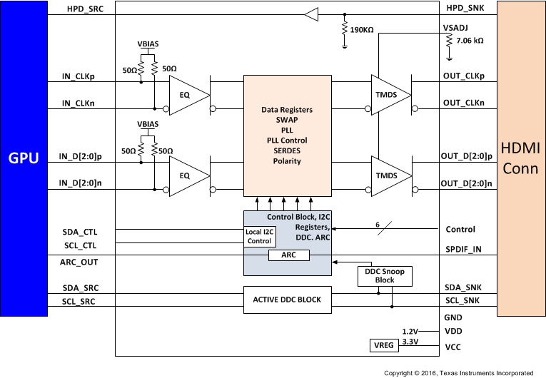
8.2 Functional Block Diagram
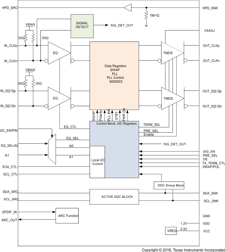
8.3 Feature Description
8.3.1 Reset Implementation
When OE is de-asserted, control signal inputs are ignored; the HDMI inputs and outputs are high impedance. It is critical to transition the OE from a low level to a high level after the VCC supply has reached the minimum recommended operating voltage. Achieve this transition by a control signal to the OE input, or by an external capacitor connected between OE and GND. To ensure the TMDS181 is properly reset, the OE pin must be de-asserted for at least 100 μs before being asserted. When OE is reasserted, the TMDS181 must be reprogrammed if it was programmed by I2C and not pin strapping. When implementing the external capacitor, the size of the external capacitor depends on the power up ramp of the VCC supply, where a slower ramp-up results in a larger-value external capacitor. Refer to the latest reference schematic for TMDS181; consider approximately 200 nF capacitor as a reasonable first estimate for the size of the external capacitor. Figure 24 and Figure 25 show both OE implementations.
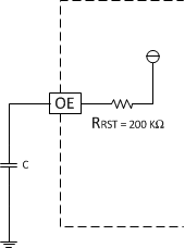 Figure 24. External Capacitor Controlled OE
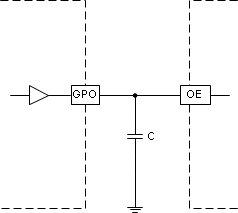 Figure 25. OE Input from Active Controller
8.3.2 Operation Timing
TMDS181 starts to operate after the OE signal is properly set after power-up timing completes. See Figure 1, Figure 2, and Power-Up and Operation Timing Requirements. If OE is held low until VDD and VCC become stable, there is no rail sequence requirement.
8.3.3 Swap and Polarity Working
TMDS181 incorporates swap function, which can set the input lanes in swap mode. The IN_D2 routes to the OUT_CLK position. The IN_D1 swaps with IN_D0. The swap function only changes the input pins. The EQ setup follows the new mapping (see Figure 26). This function can be used with the SWAP/POL pin 1 and control the register 0x09h bit 7 for SWAP enable. Lane swap function works in both redriver and retimer mode.
The TMDS181 can also swap the input polarity signals. When SWAP/POL is high the n and p pins on each lane will swap. Polarity swap only works when in retimer mode. Take care when this function is enabled and the device is in automatic crossover mode between redriver and retimer modes. When the data rate drops to the redriver level, the polarity swap is lost.
Table 2. SWAP Function(1)
| Normal Operation | SWAP = L or CSR 0x09h bit 7 is 1’b1 |
|---|---|
| IN_D2 → OUT_D2 | IN_D2 → OUT_CLK |
| IN_D1 → OUT_D1 | IN_D1 → OUT_D0 |
| IN_D0 → OUT_D0 | IN_D0 → OUT_D1 |
| IN_CLK → OUT_CLK | IN_CLK → OUT_D2 |
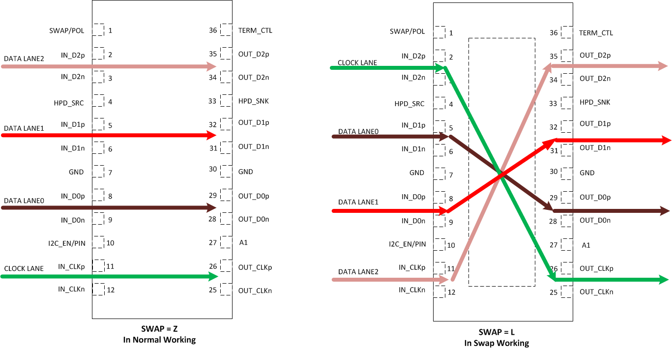 Figure 26. TMDS181 Swap Function
8.3.4 TMDS Inputs
Standard TMDS terminations are integrated on all TMDS inputs. External terminations are not required. Each input data channel contains an adaptive or fixed equalizer to compensate for cable or board losses. The voltage at the TMDS input pins must be limited below the absolute maximum ratings. An unused input should not be connected to ground because this would result in excessive current flow damaging the device. An unused input channel can be externally biased to prevent output oscillation. The complementary input pin is recommended to be grounded through a 1 kΩ resistor and the other pin left open. The input pins can be polarity changed through the local I2C register when in retimer mode.
8.3.5 TMDS Inputs Debug Tools
There are two methods for debugging a system to make sure the inputs to the TMDS181 are valid. A TMDS error checker is implemented to provide a rough bit error rate per data lane. This allows the system implementer to determine how the link between the source and TMDS181 is performing on all three data lanes. See RX PATTERN VERIFIER CONTROL/STATUS Register.
If a high error count is evident, the TMDS181 has a way to view the general eye quality. A tool is available that uses the I2C link to download the data that can be plotted for an eye diagram. This is available per data lane. This tool also provides a method to turn on an internal PRBS generator that will transmit a data signal on the data pins. A clock at the proper frequency is required on the IN_CLK pins to generate the expected output data rate.
8.3.6 Receiver Equalizer
Equalizers are used to clean up inter-symbol interference (ISI) jitter or loss from the bandwidth-limited board traces and cables. TMDS181 supports fixed receiver equalizer (Retimer and Redriver Mode) and adaptive receiver equalizer (Retimer Mode) by setting the EQ_SEL/A0 pin or through I2C reg0Ah[5]. When EQ_SEL/A0 is high, the EQ gain is fixed to 14 dB and when set low ,the EQ gain is set to 7.5 dB. TMDS181 operates in adaptive equalizer mode when the EQ_SEL/A0 pin is left floating. The EQ gain is automatically adjusted based on the data rate to compensate for trace or cable loss. Various fixed EQ values can be set through local I2C control, reg0Dh[5:1]. The fixed EQ value can be programmed for both the data and clock. Adaptive equalization is the default setting.
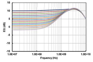 Figure 27. Adaptive EQ Gain Curve for >3.4 Gbps
8.3.7 Input Signal Detect Block
When SIG_EN is enabled, the TMDS looks for a valid TMDS clock signal input. The device is fully functional when a valid signal is detected. If no valid TMDS clock signal is detected, the device enters standby mode waiting for a valid signal at the clock input. The internal CDR is shut down and all of the TMDS outputs are in high-Z status. TMDS signal detect circuit can be set as enable by SIG_EN pin or through local I2C control but is default disabled. Implementer should activate this function in normal operation for power saving.
8.3.8 Audio Return Channel
The audio return channel in TMDS181 enables a TV, through a single HDMI cable, to send audio data upstream to an A/V receiver or surround audio controller, increasing user flexibility and eliminating the need for any separate S/PDIF audio connection. The TMDS181 supports single mode audio return channel. Customer can import the S/PDIF signal to SPDIF_IN and send out the signal from ARC_OUT and pass through the general HDMI cable to audio receiver. By I2C control, customer can disable ARC_OUT by register. Default enable after initialize.
8.3.9 Transmitter Impedance Control
HDMI2.0a standard requires a termination impedance in the 75 Ω to 150 Ω range for data rates >3.4 Gbps. Source termination is disabled at data rates <2 Gbps. When the data rate is between 2 Gbps and 3.4 Gbps, the output signal may be better if the termination value is between 150 Ω to 300 Ω, depending upon system implementation. It is important to note that there are times that this is not the best solution and no termination may be needed to pass compliance. TMDS181 supports three different source termination impedances for HDMI1.4b and HDMI2.0a. Pin 36, TX_TERM_CTL, offers a selection option to choose the output termination impedance value. This function can be programmed using I2C, reg0Bh[4:3] TX_TERM_CTL. For HDMI2.0a the 75 Ω to 150 Ω transmitter termination is required and the link will not work if this is not set.
Table 3. TX Termination Control
| PIN 36 CONFIGURATION | DESCRIPTION |
|---|---|
| TX_TERM_CTL = H | The transmitter has no termination |
| TX_TERM_CTL = L | The transmit termination impedance is approximately 75 Ω to 150 Ω to support HDMI2.0a |
| TX_TERM_CTL = NC | Automatically selects the impedance
|
8.3.10 TMDS Outputs
A 1% precision resistor, 7.06 kΩ, is recommended to be connected from VSADJ pin to ground to allow the differential output swing to comply with TMDS signal levels. The differential output driver provides a typical 10 mA current sink capability, which provides a typical 500 mV voltage drop across a 50 Ω termination resistor.
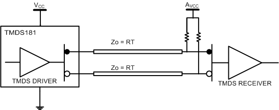 Figure 28. TMDS Driver and Termination Circuit
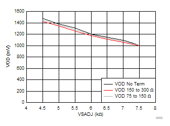
Referring to Figure 28, if VCC (TMDS181 supply) and AVCC (sink termination supply) are both powered, the TMDS output signals are high impedance when OE = high. The normal operating condition is that both supplies are active. Refer to Figure 28, if VCC is on and AVCC is off, the TMDS outputs source a typical 5-mA current through each termination resistor to ground. A total of 33 mW of power is consumed by the terminations independent of the OEB logical selection. When AVCC is powered on, normal operation (OE controls output impedance) is resumed. When the power source of the device is off and the power source to termination is on, the IO(off) output leakage current specification ensures the leakage current is limited to 45 μA or less. The VOD of the clock and data lanes can be reduced through I2C. See Table 12 for details. Figure 3 shows the different output voltages based on the different VSADJ settings.
8.3.11 Pre-Emphasis/De-Emphasis
The TMDS181 provides de-emphasis as a way to compensate for ISI loss between the TMDS181 outputs to a TMDS receiver. There are two methods to implement this function. When in pin strapping mode the PRE_SEL pin controls this function. The PRE_SEL pin provides - 2 dB or 0 dB de-emphasis, which allows the output signal pre-conditioning to offset interconnect losses from the TMDS181 device to the TMDS receiver. De-emphasis is recommended to be set at 0 dB while connecting to a receiver through short PCB route. When pulled to ground though a 65 kΩ resistor - 2 dB can be realized, see Figure 11. When using I2C, reg0Ch[1:0] is used to make these adjustments.
As there are times that true pre-emphasis may be the best solution there are two ways to accomplish this. If pin strapping is being used the best method is to reduce the VSADJ resistor value thus increasing the VOD swing and then pulling the PRE_SEL pin to ground using the 65 kΩ resistor, see Figure 29. If using I2C there are two methods to accomplish this. The first is similar to pin strapping by reducing the VSADJ resistor value and then implementing - 2 dB de-emphasis. The second method is to set reg0Ch[7:5] = 011 and set reg0Ch[1:0] = 01 which will accomplish the same pre-emphasis setting, see Figure 30.
NOTE
De-emphasis is only implement able during retimer mode. In redriver mode this function is not available.
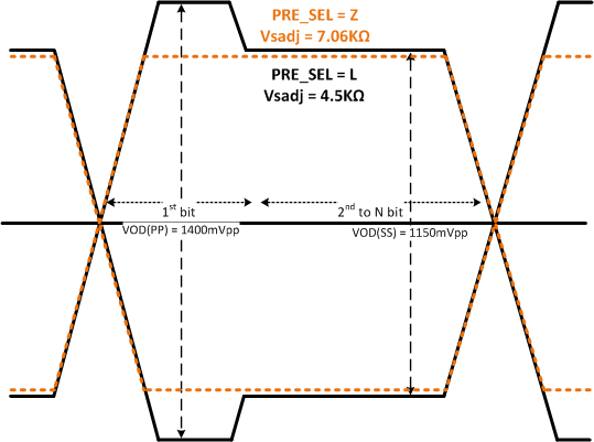 Figure 29. Output Pre-Emphasis Using Pin Strapping
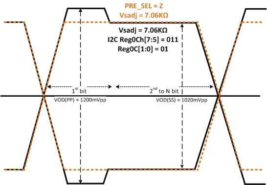 Figure 30. Output Pre-Emphasis Using I2C
8.4 Device Functional Modes
8.4.1 Retimer Mode
Clock and data recovery circuits (CDR) are used to track, sample, and retime the equalized data bit streams. The CDRs are designed with a loop bandwidth to minimize the amount of jitter transfer from the video source to the TMDS outputs. Input jitter within the CDR’s PLL bandwidth, < 1 MHz will be transferred to the TMDS outputs. Higher frequency jitter above the CDR loop bandwidth is attenuated, providing a jitter cleaning function to reduce the amount of high frequency jitter from the video source. The retimer is automatically activated at pixel clock approximately above 100 MHz when jitter cleaning is needed for robust operation when this option is enabled (default). The retimer operates at about 1 Gbps to 6 Gbps DR.
When systems switch to higher data rates above 3.4 Gbps, the CDR operates at between 85 MHz to 150 MHz pixel clock (3.4+ to 6.0 Gbps), supporting up to 4K2K high resolution with a 60 Hz refresh rate, or 3D 1080p HDTV. At pixel clock below 100 MHz, the TMDS181 automatically bypasses the internal retimer and operates as a redriver. When the video source changes resolution, the internal retimer starts the acquisition process to determine the input clock frequency and acquire lock to new data bit streams. During the clock frequency detection period and the retimer acquisition period that last approximately 7 ms, the TMDS drivers can be kept active (default) or programmed to be disabled to avoid sending invalid clock or data to the downstream receiver. The TMDS181 can be configured to work as a redriver (full range), crossover (redriver-retimer), and retimer (full range).
8.4.2 Redriver Mode
The TMDS181 also has a redriver mode that can be enabled through I2C, at reg0Ah[1:0] DEV_FUNC_MODE, which compensates for ISI channel loss. In this mode, power is reduced as the CDR and PLL are turned off. When in automatic mode, the TMDS181 is in redriver mode for data rates <1.0 Gbps. By using I2C, the device can be put in redriver mode for the complete data range of 250 Mbps to 3.4 Gbps. This is done by writing a 00 to register 0Ah[1:0]. If the link has excessive random jitter, then retimer mode is the best operating mode. When in redriver mode, the device only compensates for ISI loss. When in redriver mode compliance is not guaranteed as skew compensation and retiming functions are disabled. If a significant amount of random jitter is present, the system may not pass compliance at the connector.
8.4.3 DDC Training for HDMI2.0a Data Rate Monitor
As part of discovery, the source reads the sink’s E-EDID information to understand the capabilities of the sink. Part of this read is HDMI Forum Vendor Specific Data Block (HF-VSDB) MAX_TMDS_Character_Rate byte to determine the data rate supported. Depending upon the value, the source writes to slave address 0xA8 offset 0x20 bit1, TMDS_CLOCK_RATIO_STATUS. The TMDS181 snoops this write to determine the TMDS clock ratio and thus sets its own TMDS_CLOCK_RATIO_STATUS bit accordingly. If a 1 is written, then the TMDS clock is set to 1/40th of TMDS bit period. If a 0 is written, then the TMDS clock is set to 1/10th of TMDS bit period. The TMDS181 defaults to 1/10th of TMDS bit period unless a 1 is written to address 0xA8 offset 0x20 bit 1. When HPD is deasserted, this bit is reset to default values. If the source does not write this bit, the TMDS181 will not be configured for TMDS clock 1/40th mode in support of HDMI2.0a. As the TMDS181 is in the system link, but not recognized as part of the link, it is possible that the source could read the sink EDID where this bit is set and does not rewrite this bit. If the TMDS181 has entered a power-down state, this bit is cleared and does not re-set on a read. To work properly, the bit has to be set again with a write by the source.
8.4.4 DDC Functional Description
The TMDS181 solves sink/source level issues by implementing a master/slave control mode for the DDC bus. When the TMDS181 detects the start condition on the DDC bus from the SDA_SRC/SCL_SRC, it will transfer the data or clock signal to the SDA_SNK/SCL_SNK with little propagation delay. When SDA_SNK detects the feedback from the downstream device, the TMDS181 will pull up or pull down the SDA_SRC bus and deliver the signal to the source.
The DDC link defaults to 100 kbps but can be set to various values including 400 kbps by setting the correct value to address 0Bh through the I2C interface. The DDC lines are 5 V tolerant when the device is powered off.
NOTE
The TMDS181 utilizes clock stretching for DDC transactions. As there are sources and sinks that do not perform this function correctly a system may not work correctly as DDC transactions are incorrectly transmitted/received. To overcome this a snoop configuration can be implemented where the SDA/SCL from the source is connected directly to the SDA/SCL sink. The TMDS181 will need its SDA_SNK and SCL_SNK pins connected to this link in order to correctly configure the TMDS_CLOCK_RATIO_STATUS bit. Care must be taken when this configuration is being implemented as the voltage levels for DDC between the source and sink may be different, 3.3 V vs 5 V; See Figure 35 and See Figure 36
8.4.5 Mode Selection Functional Description
Mode selection definition: This bit lets the receiver know where the device is located in a system for the purpose of centering the AEQ point. The TMDS181 is targeting sink applications, so the default value is 1, which will center the EQ at 12 to 13 dB depending upon TMDS_CLOCK_RATIO_STATUS value (see Equalization Control Register). If the TMDS181 is in a source application, the value should be changed to a value of 0, which centers the EQ at 6.5 to 7.5 dB depending upon the TMDS_CLOCK_RATIO_STATUS value.
8.5 Register Maps
8.5.1 Local I2C Overview
The TMDS181 local I2C interface is always enabled, but will only be able to overwrite pin strapped features when I2C_EN/PIN is high. The SCL_CTL and SDA_CTL terminals are used for I2C clock and data respectively. The TMDS181 I2C interface conforms to the two-wire serial interface defined by the I2C Bus Specification, Version 2.1 (January 2000), and supports the fast mode transfer up to 400 kbps.
The device address byte is the first byte received following the START condition from the master device. The 7-bit device address for TMDS181 decides by the combination of EQ_SEL/A0 and A1. Figure 31 clarifies the TMDS181 target address.
| A1/A0 | 7 (MSB) | 6 | 5 | 4 | 3 | 2 | 1 | 0 (W/R) | HEX |
| 00 | 1 | 0 | 1 | 1 | 1 | 1 | 0 | 0/1 | BC/BD |
| 01 | 1 | 0 | 1 | 1 | 1 | 0 | 1 | 0/1 | BA/BB |
| 10 | 1 | 0 | 1 | 1 | 1 | 0 | 0 | 0/1 | B8/B9 |
| 11 | 1 | 0 | 1 | 1 | 0 | 1 | 1 | 0/1 | B6/B7 |
The typical source application of the TMDS181 is as a retimer in a TV connecting the HDMI output connector and an internal HDMI transmit through flat cables. The register setup can adjust by source side. When TMDS181 is used in a sink side application, it receives data from input connector and transmits to receiver. Local I2C buses run at 400 kHz supporting fast-mode I2C operation.
The following procedure is used to write to the TMDS181 I2C registers:
- The master initiates a write operation by generating a start condition (S), followed by the TMDS181 7-bit address and a zero-value W/R bit to indicate a write cycle.
- The TMDS181 acknowledges the address cycle.
- The master presents the sub-address (I2C register within TMDS181) to be written, consisting of one byte of data, MSB-first.
- The TMDS181 acknowledges the sub-address cycle.
- The master presents the first byte of data to be written to the I2C register.
- The TMDS181 acknowledges the byte transfer.
- The master may continue presenting additional bytes of data to be written, with each byte transfer completing with an acknowledge from the TMDS181.
- The master terminates the write operation by generating a stop condition (P).
The following procedure is used to read the TMDS181 I2C registers.
- The master initiates a read operation by generating a start condition (S), followed by the TMDS181 7-bit address and a one-value W/R bit to indicate a read cycle.
- The TMDS181 acknowledges the address cycle.
- The TMDS181 transmits the contents of the memory registers MSB-first starting at register 00h.
- The TMDS181 waits for either an acknowledge (ACK) or a not-acknowledge (NACK) from the master after each byte transfer; the I2C master acknowledges reception of each data byte transfer.
- If an ACK is received, the TMDS181 transmits the next byte of data.
- The master terminates the read operation by generating a stop condition (P).
NOTE
Upon reset, the TMDS181 sub-address is always set to 0x00. When no sub-address is included in a read operation, the TMDS181 sub-address increments from the previous acknowledged read or write data byte. If it is required to read from a sub-address that is different from the TMDS181 internal sub-address, a write operation with only a sub-address specified is needed before performing the read operation.
Refer to Local I2C Control Bit Access TAG Convention for TMDS181 local I2C register descriptions. Reads from reserved fields not described return zeros, and writes are ignored.
8.5.2 Local I2C Control Bit Access TAG Convention
Reads from reserved fields return zero, and writes to read-only reserved registers are ignored. All addresses not defined by this specification are considered reserved. Reads from these addresses return zero and writes are ignored.
BIT ACCESS TAG CONVENTIONS
A table of bit descriptions is typically included for each register description that indicates the bit field name, field description, and the field access tags. Table 4 describes the field access tags.
8.5.3 CSR Bit Field Definitions
8.5.3.1 ID Registers
Table 5. ID Registers Field Descriptions
| ADDRESS | BITS | DESCRIPTION | ACCESS |
|---|---|---|---|
| 00h~07h | 7:0 | DEVICE_ID These fields return a string of ASCII characters “TMDS181” followed by one space character. TMDS181: Address 0x00 – 0x07 = {- 0x54”T”, 0x4D”M”, 0x44”D”, 0x53”S”, 0x31”1”, 0x38”8”, 0x31”1”, 0x20}, |
R |
| 08h | 7:0 | REV _ID. This field identifies the device revision. 0000001 – TMDS181 revision 1 |
R |
8.5.3.2 MISC CONTROL Register
Table 6. MISC CONTROL Register Field Descriptions
| ADDRESS | BITS | DEFAULT | DESCRIPTION | ACCESS |
|---|---|---|---|---|
| 09h | 7 | 1’b0 | LANE_SWAP. This field swaps the input lanes as per Figure 26. 0 – Disable (default) no lane swap 1 – Enable: Swaps input lanes (redriver and retimer mode) Note: Field is loaded from SWAP/POL pin; Writes are ignored when I2C_EN/PIN = 0 |
RWU |
| 6 | 1’b0 | LANE_POLARITY swaps the input data and clock lanes polarity. 0 – Disabled (default) no polarity swap 1 – Swaps the input data and clock lane polarity (retimer mode only) Note: Field is loaded from SWAP/POL pin; Writes are ignored when I2C_EN/PIN = 0 |
RWU | |
| 5 | 1’b0 | Reserved | R | |
| 4 | 1’b0 | SIG_EN. This field enables the clock lane activity detect circuitry. (Redriver mode only because the retimer requires a clock input to work, so without a clock input, the device enters standby regardless) 0 – Disable (default) Clock detector circuit closed and receiver always works in normal operation. 1 – Enable, clock detector circuit makes the receiver automatically enter the standby state when no valid data detect. Note: Field is loaded from SIG_EN pin; Writes are ignored when I2C_EN/PIN = 0 |
RWU | |
| 3 | 1’b0 | PD_EN 0 – Normal working (default) 1 – Forced power down by I2C, lowest power state |
RW | |
| 2 | 1’b0 | HPD_AUTO_PWRDWN_DISABLE 0 – Automatically enters power-down mode based on HPD_SNK (default) 1 – Does not automatically enter power down mode |
RW | |
| 1:0 | 2’b10 | I2C_DR_CTL. I2C data rate supported for configuring device. 00 – 5 Kbps 01 – 10 Kbps 10 – 100 Kbps (default) 11 – 400 Kbps (Note: HPD_AUTO_PWRDWN_DISABLE must be set before enabling 400 Kbps mode) |
RW | |
| 0Ah | 7 | 1’b1 | Application mode selection (see Device Functional Modes) TMDS181 0 – Source 1 – Sink (default) |
RW |
| 6 | 1’b0 | HPDSNK_GATE_EN. The field sets the functional relationship between HPD_SNK and HPD_SRC. 0 – HPD_SNK passed through to the HPD_SRC (default) 1 – HPD_SNK does not pass through to the HPD_SRC. |
RW | |
| 5 | 1’b1 | EQ_ADA_EN. This field enables the equalizer functioning state. 0 – Fixed EQ 1 – Adaptive EQ (default) Writes are ignored when I2C_EN/PIN = 0 |
RWU | |
| 4 | 1’b1 | EQ_EN. This field enables the equalizer. 0 -- EQ disable 1 – EQ enable (default) Writes are ignored when I2C_EN/PIN = 0 |
RW | |
| 3 | 1’b0 | Reserved | R | |
| 2 | 1’b0 | APPLY_RXTX_CHANGES, Self-clearing write-only bit. Writing a 1 to this bit will apply new TX_TERM, HDMI_TWPST1, EQ_EN, EQ_ADA_EN, VSWING, Fixed EQ Value settings to the clock and data lanes. Writes to the respective registers do not take immediate effect. This bit does not need to be written if I2C configuration occurs while HPD_SNK are low, I2CPD_EN = 1 or there is no HDMI clock applied and SIGN_EN is high. |
W | |
| 1:0 | 2’b01 | DEV_FUNC_MODE. This field selects the device working function mode. 00 – Redriver mode: 250 Mbps – 3.4 Gbps 01 – Automatic redriver to retimer crossover at 1.0 Gbps (default) 10 – Automatic retimer when HDMI2.0a based upon TMDS_CLOCK_RATIO_STATUS 11 – Retimer mode across full range 250 Mbps to 6 Gbps When changing crossover point, need to toggle PD_EN or toggle external HPD_SNK. |
RW | |
| 0Bh | 7:5 | 3’b000 | Reserved | R |
| 4:3 | 2'b00 | TX_TERM_CTL. Controls termination for HDMI TX. 00 – No termination (default) 01 – 150 Ω to 300 Ω 10 – Reserved 11 – 75 Ω to 150 Ω Note: Writes are ignored when I2C_EN/PIN = 0; reflects the value of TX_TERM_CTL pin. |
RWU | |
| 2 | 1'b0 | DDC_DR_SEL Defines the DDC output speed for DDC bridge 0 = 100 kbps (default) 1 = 400 kbps (Note: HPD_AUTO_PWRDWN_DISABLE must be set before enabling 400 Kbps mode) |
RW | |
| 1 | 1'b0 | TMDS_CLOCK_RATIO_STATUS. This field is updated from snoop of DDC write to slave address 0xA8 offset 0x20 bit 1 that occurred on the SDA_SRC/SCL_SRC interface. When bit 1 of address 0xA8 offset 0x20 in the SCDC register set is written to a 1’b1, then this field will be set to a 1’b1. When bit 1 of address 0xA8 offset 0x20 is written to a 1’b0, then this field will be set to a 1’b0. This field is reset to default value whenever HPD_SNK is de-asserted for greater than 2 ms. 0 – TMDS Clock is 1/10 of TMDS bit period (default) 1 – TMDS Clock is 1/40 of TMDS bit period |
RWU | |
| 0 | 1'b0 | DDC_TRAIN_SETDISABLE; This field indicate the DDC training block function status. If disabled the device will only work in HDMI1.x or DVI modes. 0 – DDC training enable (default) 1 – DDC training disable Note: To force TMDS_CLOCK_RATIO_STATUS to 1 this register bit must be set to 1 which will force the 1/40 mode for HDMI2.0 |
RW | |
| 0Ch | 7:5 | 3’b000 | VSWING_DATA: Data output swing control 000 – Vsadj set (default) 001 – Increase by 7% 010 – Increase by 14% 011 – Increase by 21% 100 – Decrease by 30% 101 – Decrease by 21% 110 – Decrease by 14% 111 – Decrease by 7% |
RW |
| 4:2 | 3’b000 | VSWING_CLK: Clock output swing control: Default is set by Vsadj resistor value and the value of reg_0Dh[0]. 000 – Vsadj (default) 001 – Increase by 7% 010 – Increase by 14% 011 – Increase by 21% 100 – Decrease by 30% 101 – Decrease by 21% 110 – Decrease by 14% 111 – Decrease by 7% |
RW | |
| 1:0 | 2’b00 | HDMI_TWPST1[1:0]. HDMI de-emphasis FIR post-cursor-1 signed tap weight. (Retimer Mode Only) 00 – No de-emphasis (default) 01 – 2 dB de-emphasis 10 – Reserved 11 – Reserved Note: Reflects value of PRE_SEL pin; Writes are ignored when I2C_EN/PIN = 0 |
RWU |
8.5.3.3 Equalization Control Register
Table 7. Equalization Control Register Field Descriptions
| ADDRESS | BITS | DEFAULT | DESCRIPTION | ACCESS | |
|---|---|---|---|---|---|
| 0Dh | 7:6 | 2’b00 | Reserved | R | |
| 5:3 | 1’b000 | Data lane EQ – Sets fixed EQ values | RW | ||
| HDMI1.x | HDMI2.0a | ||||
| 000 – 0 dB (default) | 000 – 0 dB (default) | ||||
| 001 – 4.5 dB | 001 – 3 dB | ||||
| 010 – 6.5 dB | 010 – 5 dB | ||||
| 011 – 8.5 dB | 011 – 7.5 dB | ||||
| 100 – 10.5 dB | 100 – 9.5 dB | ||||
| 101 – 12 dB | 101 – 11 dB | ||||
| 110 – 14 dB | 110 – 13 dB | ||||
| 111 – 16.5 dB | 111 – 14.5 dB | ||||
| 2:1 | 1’b00 | Clock lane EQ - Sets fixed EQ values | RW | ||
| HDMI1.x | HDMI2.0a | ||||
| 00 – 0 dB (default) | 00 – 0 dB (default) | ||||
| 01 – 1.5 dB | 01 – 1.5 dB | ||||
| 10 – 3 dB | 10 – 3 dB | ||||
| 11 – RSVD | 11 – 4.5 dB | ||||
| 0 | 1’b0 | DIS_HDMI2_SWG: 0 – Clock VOD is half of set values when TMDS_CLOCK_RATIO_STATUS states in HDMI2.0a mode (default) 1 – Disables TMDS_CLOCK_RATIO_STATUS control of the clock VOD so output swing is at full swing. |
RW | ||
8.5.3.4 RX PATTERN VERIFIER CONTROL/STATUS Register
Table 8. RX PATTERN VERIFIER CONTROL/STATUS Register Field Description(1)
9 Application and Implementation
NOTE
Information in the following applications sections is not part of the TI component specification, and TI does not warrant its accuracy or completeness. TI’s customers are responsible for determining suitability of components for their purposes. Customers should validate and test their design implementation to confirm system functionality.
9.1 Application Information
The TMDS181 was defined to work in many applications. This includes source applications like a Blu-ray™ DVD player or AVR. The adaptive receive equalizer makes it ideal for sink applications like UHDTV, monitors, and projectors where cable length can be widely varied. When in a sink application, the designer must consider several system-level architectures. The TMDS181 is also capable of working in an active cable to extend the cable length even further.
9.2 Typical Applications
9.2.1 Source Side Application
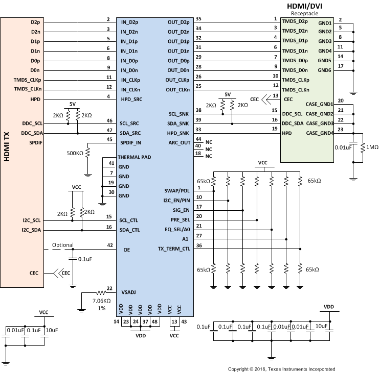 Figure 32. TMDS181 in Source Side Application
9.2.1.1 Design Requirements
The TMDS181 can be designed into many different applications. All applications have certain requirements for the system to work properly. Two voltage rails are required to support the lowest power consumption possible. The OE pin must have a 0.1 µF capacitor to ground. This pin can be driven by a processor, but the pin needs to change states after voltage rails have stabilized. The best way to configure the device is by using I2C. However, pin strapping is provided because I2C is not available in all cases. As sources may have different naming conventions, it is necessary to confirm that the link between the source and the TMDS181 are correctly mapped. A swap function is provide for the input pins in case signaling is reversed between source and device. The control pin values in Table 9 are based upon driving pins with a microcontroller; otherwise, the shown pullup/pulldown configuration meet device levels. Table 9 provides information on expected values in order to perform properly.
Table 9. Design Parameters
| DESIGN PARAMETER | VALUE |
|---|---|
| VCC | 3.3 V |
| VDD | 1.2 V |
| Main link input voltage | VID = 75 mVpp to 1.2 Vpp |
| Control pin max voltage for low | 65 kΩ resistor connected to GND |
| Control pin voltage range mid | Not connected |
| Control pin min voltage for high | 65 kΩ resistor connected to Vcc |
| VSADJ resistor | 7.06 kΩ 1% |
9.2.1.2 Detailed Design Procedure
The TMDS181 is a signal conditioning device that provides several forms of signal conditioning to support compliance for HDMI or DVI at a source connector. These forms of signal conditioning are accomplished using receive equalization, retiming, and output driver configure ability. The transmitter drives 2 to 3 inches of board trace and connector when compliance is required at the connector.
To design in the TMDS181 for a source side application, the designer must understand the following.
- Determine the loss profile between the GPU/chipset and the HDMI/DVI connector.
- Based upon this loss profile and signal swing, determine the optimal location for the TMDS181 in order to pass source electrical compliance, usually within 2 to 3 inches of the connector.
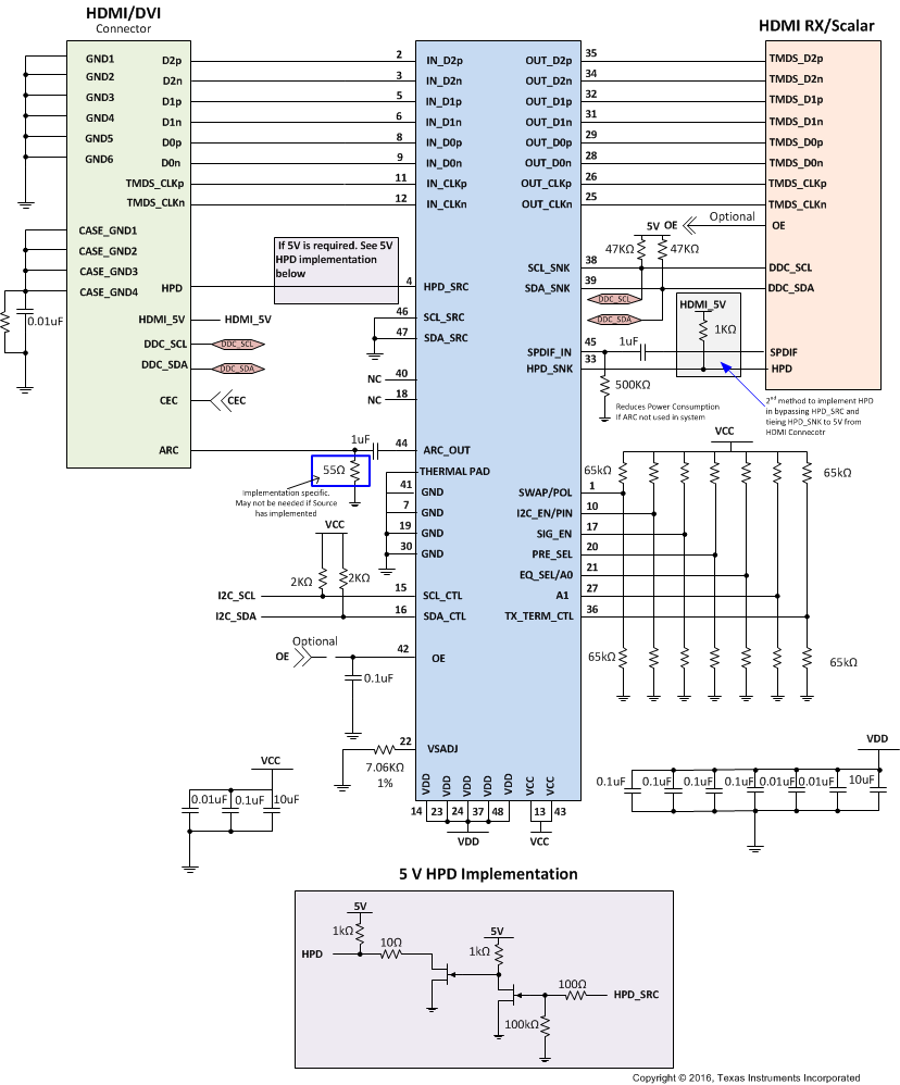
- Use the typical application Figure 32 for information on control pin resistors.
- The TMDS181 has a receiver adaptive equalizer, but can also be configured using EQ_SEL control pin.
- Set the VOD, pre-emphasis and termination levels appropriately to support compliance by using the appropriate VSADJ resistor value and setting PRE_SEL and TX_TERM_CTL control pins.
- The thermal pad must be connected to ground.
- See schematics in Figure 32 on recommended decoupling capacitors from VCC pins to ground.
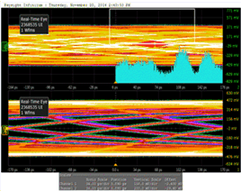
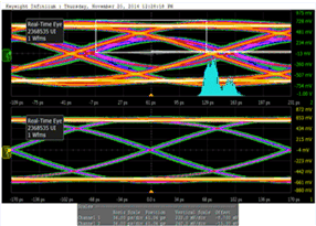
9.2.1.3 Application Curves
9.2.2 Sink Side Application
For a sink side application, HPD needs consideration. The TMDS181 drives the HPD signal to 3.3 V, which meets requirements, but if 5 V HPD signaling is required, the two circuits shown in Figure 35 are required. As sources are not consistent in implementing all aspects of the DDC link, TI recommends to configure the TMDS181 as per Figure 35. Another consideration for how HPD is implemented is the architecture and behavior of the HDMI RX/scalar. The standard requires sinks to clear the TMDS_CLOCK_RATIO_STATUS in the SCDC when either +5 V power signal from source is not present or when hot plug detect pin goes low for 100 ms or more. When HPD goes low, the TMDS181 automatically clears this bit. The TMDS181 expects the TMDS_CLOCK_RATIO_STATUS bit to be set with a write from source to receiver/sink. If this does not happen, the TMDS181 may come up in the wrong configuration. Until the HDMI ecosystem matures, TI recommends to implement sink application as per Figure 36 to address this.
Designing the TMDS181 into a sink side application requires similar care as for a source side application. However, because compliance is at the receiver, there is more flexibility for the transmitter to the HDMI RX/chipset link. Because many different reflection points are possible, the TMDS181 allows for swing, pre-emphasis, and transmitter termination control that can help minimize these reflections. The TMDS181 has a 3.3 V HPD drive capability which meets requirements. In cases where the designer needs to support 5 V HPD drive capability, the circuit shown in Figure 35 is required.
To design in the TMDS181 for a source side application, the designer must understand the following.
- Determine the loss profile between the RX/chipset and the HDMI/DVI connector
- Based upon this loss profile and signal swing, determine the optimal location for the TMDS181 to pass sink electrical compliance.
- Use the typical application Figure 35 for information on control pin resistors.
- The TMDS181 has a receiver adaptive equalizer, but can also be configured using EQ_SEL control pin.
- Set the VOD, pre-emphasis and termination levels appropriately to support a link between TMDS181 and HDMI RX/chipset by using the appropriate VSADJ resistor value and setting PRE_SEL and TX_TERM_CTL control pins.
- The thermal pad must be connected to ground.
- See schematics in Figure 35 on recommended decoupling capacitors from VCC pins to ground.
- Because the HDMI ecosystem supporting 4k2kp60 is not mature, TI recommends to design the TMDS181 into the sink application as shown in Figure 36.
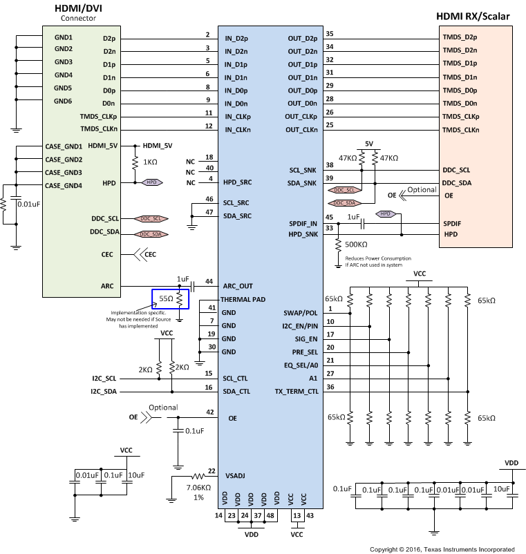 Figure 36. TMDS181 in Sink Side Application
9.2.3 Application Chain Showing DDC Connections
The DDC circuitry inside the TMDS181 allows multiple stage operation (see Figure 36). The retimer devices can be connected to any of the bus segments. The number of devices that can be connected in series is limited by repeater delay/time of flight considerations for the maximum bus speed requirements.
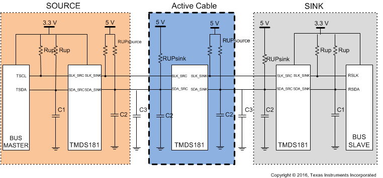 Figure 37. Typical Series Application
9.2.3.1 Detailed Design Procedure
9.2.3.1.1 DDC Pullup Resistors
NOTE
This section is informational only and subject to change depending upon the specific system implementation.
The pullup resistor value is determined by two requirements.
- The maximum sink current of the I2C buffer: The maximum sink current is 3 mA or slightly higher for an I2C driver supporting standard-mode I2C operation.
- The maximum transition time on the bus: The maximum transition time, T, of an I2C bus is set by an RC time constant. The parameter, k, can be calculated from Equation 3 by solving for t, the times at which certain voltage thresholds are reached. Different input threshold combinations introduce different values of t. Table 10 summarizes the possible values of k under different threshold combinations.
- R is the pullup resistor value.
- C is the total load capacitance.

where

Table 10. Value k upon Different Input Threshold Voltages
| Vth–\Vth+ | 0.7VCC | 0.65VCC | 0.6VCC | 0.55VCC | 0.5VCC | 0.45VCC | 0.4VCC | 0.35VCC | 0.3VCC |
|---|---|---|---|---|---|---|---|---|---|
| 0.1VCC | 1.0986 | 0.9445 | 0.8109 | 0.6931 | 0.5878 | 0.4925 | 0.4055 | 0.3254 | 0.2513 |
| 0.15VCC | 1.0415 | 0.8873 | 0.7538 | 0.6360 | 0.5306 | 0.4353 | 0.3483 | 0.2683 | 0.1942 |
| 0.2VCC | 0.9808 | 0.8267 | 0.6931 | 0.5754 | 0.4700 | 0.3747 | 0.2877 | 0.2076 | 0.1335 |
| 0.25VCC | 0.9163 | 0.7621 | 0.6286 | 0.5108 | 0.4055 | 0.3102 | 0.2231 | 0.1431 | 0.0690 |
| 0.3VCC | 0.8473 | 0.6931 | 0.5596 | 0.4418 | 0.3365 | 0.2412 | 0.1542 | 0.0741 |
From Equation 1, Rup(min) = 5.5 V / 3 mA = 1.83 kΩ to operate the bus under a 5 V pullup voltage and provide <3 mA when the I2C device is driving the bus to a low state. If a higher sink current, for example 4 mA, is allowed, Rup(min) can be as low as 1.375 kΩ. If DDC working at standard mode of 100 Kbps, the maximum transition time T is fixed, 1 μs, and using the k values from Table 10, the recommended maximum total resistance of the pullup resistors on an I2C bus can be calculated for different system setups. If DDC working in fast mode of 400 Kbps, the transition time should be set at 300 ns according to I2C specification. To support the maximum load capacitance specified in the HDMI specification, calculate Ccable(max) = 700 pF / Csource = 50 pF / Ci = 50 pF, R(max) as shown in Table 11.
Table 11. Pullup Resistor Upon Different Threshold Voltages and 800 pF Loads
| Vth-\Vth+ | 0.7VCC | 0.65VCC | 0.6VCC | 0.55VCC | 0.5VCC | 0.45VCC | 0.4VCC | 0.35VCC | 0.3VCC | UNIT |
|---|---|---|---|---|---|---|---|---|---|---|
| 0.1VCC | 1.14 | 1.32 | 1.54 | 1.8 | 2.13 | 2.54 | 3.08 | 3.84 | 4.97 | kΩ |
| 0.15VCC | 1.2 | 1.41 | 1.66 | 1.97 | 2.36 | 2.87 | 3.59 | 4.66 | 6.44 | kΩ |
| 0.2VCC | 1.27 | 1.51 | 1.8 | 2.17 | 2.66 | 3.34 | 4.35 | 6.02 | 9.36 | kΩ |
| 0.25VCC | 1.36 | 1.64 | 1.99 | 2.45 | 3.08 | 4.03 | 5.6 | 8.74 | 18.12 | kΩ |
| 0.3VCC | 1.48 | 1.8 | 2.23 | 2.83 | 3.72 | 5.18 | 8.11 | 16.87 | — | kΩ |
To accommodate the 3-mA drive current specification, a narrower threshold voltage range is required to support a maximum 800-pF load capacitance for a standard-mode I2C bus.
9.2.3.1.2 Compliance Testing
Compliance testing is very system design specific. Properly designing the system and configuring the TMDS181 can help pass compliance for a system. The following information is a starting point to help prepare for compliance testing. As each system is different there are many features in the TMDS181 to help tune the circuit. These include fixed RX equalization, adaptive RX equalization, VOD adjust by several methods, pre-emphasis/de-emphasis, and source termination. Passing both HDMI2.0a and HDMI1.4b compliance is easier to accomplish when using I2C as this provides more fine tuning capability.
9.2.3.1.2.1 Pin Strapping Configuration for HDMI2.0a and HDMI1.4b
9.2.3.1.2.2 I2C Control for HDMI2.0a and HDMI1.4b
- VSADJ Resistor = 7.06 kΩ: This value may be changed in order to improve Intra-pair skew but will increase VOD so care must be taken to avoid VOD and VL compliance issues. The VOD can be increased or decreased by using I2C Reg0Ch[7:2]
- PRE_SEL = Reg0Ch[1:0] = 01 for -2 dB (Labeled HDMI_TWPST)
- TX_TERM_CTL = NC for Auto Select.
- Reg0Bh[4:3] = 00 → No TX Term; HDMI1.4b < 2 Gbps (This may be best value for all HDMI1.4b)
- Reg0Bh[4:3] = 01 → 150 Ω to 300 Ω; HDMI1.4b > 2 Gbps
- Reg0Bh[4:3] = 11 → 75 Ω to 150 Ω; HDMI2.0a
10 Power Supply Recommendations
To minimize the power consumption of customer application, TMSD181 used the dual power supply. VCC is 3.3 V with 5% range to support the I/O voltage. VDD is 1.2 V to supply the internal digital control circuit. TMDS181 operates in three different working states.
- Power-down mode:
- OE = Low puts the device into its lowest power state by shutting down all function blocks.
- When OE is reasserted, the transitions from L → H create a reset, and if the device is programmed through I2C, it must be reprogrammed.
- Writing a 1 to register 09h[3].
- OE = High, HPD_SNK = Low
- OE = Low puts the device into its lowest power state by shutting down all function blocks.
- Standby mode: HPD_SNK = High, but no valid clock signal detect on clock lane.
- Normal operation: Working in redriver or retimer
- When HPD asserts, the device CDR and output enables based on the signal detector circuit result.
- HPD_SRC = HPD_SNK in all conditions. The HPD channel is operational when VCC is over 3 V.
NOTE
- When the TMDS181 is put into a power-down state, the I2C registers are cleared. This is important as the TMDS_CLOCK_RATIO_STATUS bit will be cleared. If cleared and HDMI2.0 resolutions are to be supported, the TMDS181 expects the source to write a 1 to this bit location. If this does not happen, the PLL will not be set properly and no video may be evident.
- Power performance of the TMDS181 is highly dependent upon the HDMI transmitter architecture driving the TMDS181 receiver. The TMDS181 has integrated the termination resistors, which increases the power consumption on the 3.3 V rail by as much as 400 mW. This is the power required by the HDMI transmitter to switch and not needed by the TMDS181 to operate properly.
Table 12. Power-Up and Operation Timing Requirements
| INPUTS | STATUS | ||||||||||
|---|---|---|---|---|---|---|---|---|---|---|---|
| HPD_SNK | OE | SIG_EN | IN_CLK | DATA RATE | HPD_SRC | IN_Dx | SDA/SCL_CTL | OUT_Dx OUT_CLK |
DDC | ARC | MODE |
| X | L | H or L | X | X | H | RX Termination On | Disable | High-Z | Disabled | Disable | Power-down mode |
| L | H | H or L | X | X | L | RX Termination On | Active | High-Z | Disabled | Disable | Power-down mode |
| H | H | H or L | X | X | H | RX Termination On | Active | High-Z | Disabled | Disable | Power-down mode by W 1 to 09h[3] |
| H | H | H (no valid signal) |
No valid TMDS clock | X | H | D0-D2 disabled with RX termination On, IN_CLK active | Active | High-Z | Active | Active | Standby mode (squelch waiting) |
| H | H | H or L (no valid signal) |
No valid TMDS clock | Retimer mode | H | D0-D2 disabled with RX termination On, IN_CLK activee | Active | High-Z | Active | Active | Standby mode (Squelch waiting) |
| H | H | H (Valid signal) |
Valid TMDS clock | Retimer mode | H | RX active | Active | TX active | Active | Active | Normal operation |
| H | H | L (no valid signal) |
No valid TMDS clock | Redriver mode | H | RX active | Active | TX active | Active | Active | Normal operation |
| H | H | H (Valid signal) |
Valid TMDS clock | Redriver mode | H | RX active | Active | TX active | Active | Active | Normal operation |

