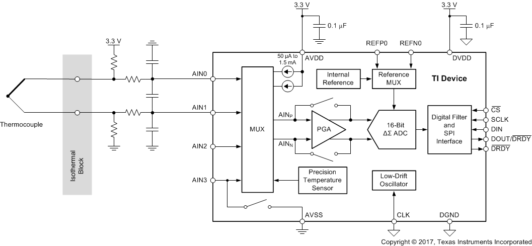
-
具有集成 PGA 和基准的 ADS1120 4 通道、2kSPS、低功耗、16 位 ADC
- 1 特性
- 2 应用
- 3 说明
- 4 修订历史记录
- 5 Pin Configuration and Functions
- 6 Specifications
- 7 Parameter Measurement Information
-
8 Detailed Description
- 8.1 Overview
- 8.2 Functional Block Diagram
- 8.3 Feature Description
- 8.4 Device Functional Modes
- 8.5 Programming
- 8.6 Register Map
- 9 Application and Implementation
- 10Power Supply Recommendations
- 11Layout
- 12器件和文档支持
- 13机械、封装和可订购信息
- 重要声明
具有集成 PGA 和基准的 ADS1120 4 通道、2kSPS、低功耗、16 位 ADC
1 特性
- 低电流消耗:
占空比模式下低至 120μA(典型值) - 宽电源范围:2.3V 至 5.5V
- 可编程增益:1V/V 至 128V/V
- 可编程数据速率:高达 2kSPS
- 16 位无噪声分辨率(20SPS 时)
- 采用单周期稳定数字滤波器,在 20SPS 时
实现 50Hz 和 60Hz 谐波抑制 - 两个差分输入或四个单端输入
- 双匹配可编程电流源:50μA 至 1.5mA
- 内部 2.048V 基准电压:漂移 5ppm/°C(典型值)
- 集成 2% 精准振荡器
- 集成温度传感器:精度 0.5°C(典型值)
- 与 SPI 兼容的接口(模式 1)
- 封装:3.5mm × 3.5mm × 0.9mm 超薄型四方扁平无引线 (VQFN)
2 应用
- 温度传感器测量:
- 热敏电阻
- 热电偶
- 电阻式温度检测器 (RTD):
2 线、3 线或 4 线制类型
- 电阻桥式传感器测量:
- 压力传感器
- 应力计
- 衡器
- 便携式仪表
- 工厂自动化和过程控制
3 说明
ADS1120 是一款 16 位高精度模数转换器 (ADC),集成了多种 特性, 能够降低系统成本并减少小型传感器信号测量 应用 中的组件数量。该器件 具有 通过输入多路复用器 (MUX) 实现的两个差分输入或四个单端输入,一个低噪声可编程增益放大器 (PGA),两个可编程激励电流源,一个电压基准,一个振荡器,一个低侧开关和一个精密温度传感器。
此器件能够以高达 2000 次/秒 (SPS) 采样数据速率执行转换,并且能够在单周期内稳定。针对噪声环境中的工业应用,当采样频率为 20SPS 时,数字滤波器可同时提供 50Hz 和 60Hz 抑制。内部 PGA 提供高达 128V/V 的增益。此 PGA 使得 ADS1120 非常适用于小型传感器信号测量 应用 ,例如电阻式温度检测器 (RTD)、热电偶、热敏电阻和桥式传感器。该器件在使用 PGA 时支持测量伪差分或全差分信号。此外,该器件还可配置为禁用内部 PGA,同时仍提供高输入阻抗和高达 4V/V 的增益,从而实现单端测量。
在禁用 PGA 后的占空比模式下运行功耗可低至 120µA。ADS1120 采用无引线 VQFN-16 或薄型小外形尺寸 (TSSOP)-16 封装,额定工作温度范围为 -40°C 至 +125°C。
器件信息(1)
| 器件型号 | 封装 | 封装尺寸(标称值) |
|---|---|---|
| ADS1120 | VQFN (16) | 3.50mm x 3.50mm |
| TSSOP (16) | 5.00mm x 4.40mm |
- 如需了解所有可用封装,请见数据表末尾的可订购产品附录。
4 修订历史记录
Changes from B Revision (January 2015) to C Revision
- Changed 文档标题Go
- Changed K 型热电偶测量图Go
- Added footnote 1 to Pin Functions table and changed descriptions of AIN0/REFP1, AIN1, AIN2, AIN3/REFN1, REFN0, and REFP0 pins accordingly Go
- Changed format of Absolute Maximum Ratings tableGo
- Changed Functional Block Diagram figure Go
- Changed Bypassing the PGA sectionGo
- Changed (AVDD) to (AVDD – AVSS) in first paragraph of Voltage Reference sectionGo
- Added fourth sentence to Temperature Sensor sectionGo
- Changed last equation in Converting from Digital Codes to Temperature sectionGo
- Changed bit 0 in register 03h to 0 from RESERVED Go
- Changed description of bits 5:4 in Configuration Register 2Go
- Added Unused Inputs and Outputs section Go
- Changed Thermocouple Measurement figureGo
- Changed 3-Wire RTD Measurement figure Go
- Changed 2-Wire RTD Measurement figure Go
- Changed 4-Wire RTD Measurement figure Go
- Changed Resistive Bridge Measurement figure Go
- Changed Power Supply Recommendations section: changed Power-Supply Sequencing subsection, added Power-Supply Ramp Rate subsectionGo
Changes from A Revision (January 2014) to B Revision
- 增加了 ESD 额定值表、推荐的运行条件表、应用和实施、电源相关建议、布局、器件和文档支持以及机械、封装和可订购信息部分Go
- 更改了文档标题、特性, 应用, 说明,引脚配置和功能,参数测量信息,特性 说明,器件功能模式,编程,寄存器映射部分以及首页图Go
- Deleted Ordering Information section and Product Family tableGo
- Changed format of Absolute Maximum Ratings table and added minimum junction temperature specificationGo
- Changed Analog Inputs and Voltage Reference Input sections (specification values were not changed) and added Internal Oscillator section to Electrical Characteristics tableGo
- Changed System Performance section: changed VIO parameter name, deleted symbol and changed test conditions of Gain error parameter in Electrical Characteristics table Go
- Deleted Clock Sources section and changed Temperature Sensor and Power Supply sections (specification values were not changed) in Electrical Characteristics tableGo
- Changed SPI Timing Requirements and Figure 1 (specification values were not changed), added SPI Switching Characteristics and Figure 2 Go
- Changed format of Typical Characteristics section (actual curves did not change)Go
Changes from * Revision (August 2013) to A Revision
- 投入生产Go
5 Pin Configuration and Functions
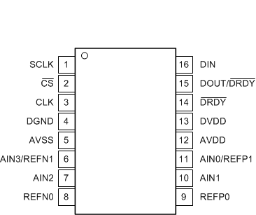
Pin Functions
| PIN | ANALOG OR DIGITAL INPUT/OUTPUT |
DESCRIPTION(1) | ||
|---|---|---|---|---|
| NAME | NO. | |||
| RVA | PW | |||
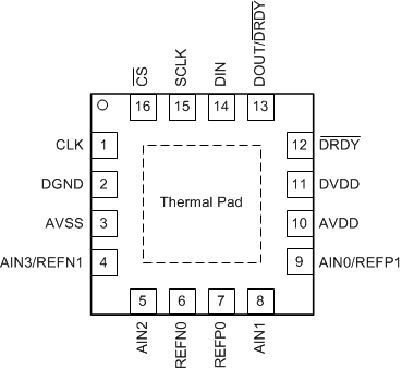
| AIN0/REFP1 | 9 | 11 | Analog input | Analog input 0, positive reference input 1 |
| AIN1 | 8 | 10 | Analog input | Analog input 1 |
| AIN2 | 5 | 7 | Analog input | Analog input 2 |
| AIN3/REFN1 | 4 | 6 | Analog input | Analog input 3, negative reference input 1. Internal low-side power switch connected between AIN3/REFN1 and AVSS. |
| AVDD | 10 | 12 | Analog | Positive analog power supply |
| AVSS | 3 | 5 | Analog | Negative analog power supply |
| CLK | 1 | 3 | Digital input | External clock source pin. Connect to DGND if not used. |
| CS | 16 | 2 | Digital input | Chip select; active low. Connect to DGND if not used. |
| DGND | 2 | 4 | Digital | Digital ground |
| DIN | 14 | 16 | Digital input | Serial data input |
| DOUT/DRDY | 13 | 15 | Digital output | Serial data output combined with data ready; active low |
| DRDY | 12 | 14 | Digital output | Data ready, active low. Leave unconnected or tie to DVDD using a weak pull-up resistor if not used. |
| DVDD | 11 | 13 | Digital | Positive digital power supply |
| REFN0 | 6 | 8 | Analog input | Negative reference input 0 |
| REFP0 | 7 | 9 | Analog input | Positive reference input 0 |
| SCLK | 15 | 1 | Digital input | Serial clock input |
| Thermal pad | — | — | Thermal power pad. Do not connect or only connect to AVSS. | |
6 Specifications
6.1 Absolute Maximum Ratings(1)
6.2 ESD Ratings
| VALUE | UNIT | |||
|---|---|---|---|---|
| V(ESD) | Electrostatic discharge | Human-body model (HBM), per ANSI/ESDA/JEDEC JS-001(1) |
±2000 | V |
| Charged-device model (CDM), per JEDEC specification JESD22-C101(2) |
±500 | |||
6.3 Recommended Operating Conditions
over operating ambient temperature range (unless otherwise noted)| MIN | NOM | MAX | UNIT | |||
|---|---|---|---|---|---|---|
| POWER SUPPLY | ||||||
| Unipolar analog power supply | AVDD to AVSS | 2.3 | 5.5 | V | ||
| AVSS to DGND | –0.1 | 0 | 0.1 | |||
| Bipolar analog power supply | AVDD to DGND | 2.3 | 2.5 | 2.75 | V | |
| AVSS to DGND | –2.75 | –2.5 | –2.3 | |||
| Digital power supply | DVDD to DGND | 2.3 | 5.5 | V | ||
| ANALOG INPUTS(1) | ||||||
| VIN | Differential input voltage | VIN = V(AINP) – V(AINN)(2) | –Vref / Gain | Vref / Gain | V | |
| V(AINx) | Absolute input voltage | PGA disabled, gain = 1 to 4 | AVSS – 0.1 | AVDD + 0.1 | V | |
| PGA enabled, gain = 1 to 128 | See the Low-Noise PGA section | |||||
| VCM | Common-mode input voltage | PGA disabled, gain = 1 to 4 | AVSS – 0.1 | AVDD + 0.1 | V | |
| PGA enabled, gain = 1 to 128 | See the Low-Noise PGA section | |||||
| VOLTAGE REFERENCE INPUTS(3) | ||||||
| Vref | Differential reference input voltage | Vref = V(REFPx) – V(REFNx) | 0.75 | 2.5 | AVDD | V |
| V(REFNx) | Absolute negative reference voltage | AVSS – 0.1 | V(REFPx) – 0.75 | V | ||
| V(REFPx) | Absolute positive reference voltage | V(REFNx) + 0.75 | AVDD + 0.1 | V | ||
| EXTERNAL CLOCK SOURCE | ||||||
| f(CLK) | External clock frequency | 0.5 | 4.096 | 4.5 | MHz | |
| Duty cycle | 40% | 60% | ||||
| DIGITAL INPUTS | ||||||
| Input voltage | DGND | DVDD | V | |||
| TEMPERATURE RANGE | ||||||
| TA | Operating ambient temperature | –40 | 125 | °C | ||
PGA disabled means the low-noise PGA is powered down and bypassed. Gains of 1, 2, and 4 are still possible in this case.
See the Bypassing the PGA section for more information.
Limited to ±[(AVDD – AVSS) – 0.4 V] / Gain, when the PGA is enabled.
6.4 Thermal Information
| THERMAL METRIC(1) | ADS1120 | UNIT | ||
|---|---|---|---|---|
| VQFN (RVA) | TSSOP (PW) | |||
| 16 PINS | 16 PINS | |||
| RθJA | Junction-to-ambient thermal resistance | 43.4 | 99.5 | °C/W |
| RθJC(top) | Junction-to-case (top) thermal resistance | 47.3 | 35.2 | °C/W |
| RθJB | Junction-to-board thermal resistance | 18.4 | 44.3 | °C/W |
| ψJT | Junction-to-top characterization parameter | 0.6 | 2.4 | °C/W |
| ψJB | Junction-to-board characterization parameter | 18.4 | 43.8 | °C/W |
| RθJC(bot) | Junction-to-case (bottom) thermal resistance | 2.0 | n/a | °C/W |
6.5 Electrical Characteristics
Minimum and maximum specifications apply from TA = –40°C to +125°C. Typical specifications are at TA = 25°C.All specifications are at AVDD = 3.3 V, AVSS = 0 V, DVDD = 3.3 V, PGA enabled, DR = 20 SPS, and external Vref = 2.5 V (unless otherwise noted).(1)
| PARAMETER | TEST CONDITIONS | MIN | TYP | MAX | UNIT | ||
|---|---|---|---|---|---|---|---|
| ANALOG INPUTS | |||||||
| Absolute input current | See the Typical Characteristics | ||||||
| Differential input current | See the Typical Characteristics | ||||||
| SYSTEM PERFORMANCE | |||||||
| Resolution (no missing codes) | 16 | Bits | |||||
| DR | Data rate | Normal mode | 20, 45, 90, 175, 330, 600, 1000 | SPS | |||
| Duty-cycle mode | 5, 11.25, 22.5, 44, 82.5, 150, 250 | ||||||
| Turbo mode | 40, 90, 180, 350, 660, 1200, 2000 | ||||||
| Noise (input-referred) | See the Noise Performance section | ||||||
| INL | Integral nonlinearity | Gain = 1 to 128, VCM = 0.5 AVDD, best fit(2) | 8 | 20 | ppmFSR | ||
| VIO | Input offset voltage | PGA disabled, gain = 1 to 4, differential inputs | ±4 | µV | |||
| Gain = 1 to 128, differential inputs | ±4 | ||||||
| Offset drift | PGA disabled, gain = 1 to 4 | 0.25 | µV/°C | ||||
| Gain = 1 to 128, TA = –40°C to +85°C(2) | 0.08 | 0.3 | |||||
| Gain = 1 to 128 | 0.25 | ||||||
| Gain error | PGA disabled, gain = 1 to 4 | ±0.015% | |||||
| Gain = 1 to 128, TA = 25°C | –0.1% | ±0.015% | 0.1% | ||||
| Gain drift | PGA disabled, gain = 1 to 4 | 1 | ppm/°C | ||||
| Gain = 1 to 128(2) | 1 | 4 | |||||
| NMRR | Normal-mode rejection ratio(2) | 50 Hz ±3%, DR = 20 SPS, external CLK, 50/60 bit = 10 | 105 | dB | |||
| 60 Hz ±3%, DR = 20 SPS, external CLK, 50/60 bit = 11 | 105 | ||||||
| 50 Hz or 60 Hz ±3%, DR = 20 SPS, external CLK, 50/60 bit = 01 |
90 | ||||||
| CMRR | Common-mode rejection ratio | At dc, gain = 1 | 90 | 105 | dB | ||
| f(CM) = 50 Hz, DR = 2000 SPS(2) | 95 | 115 | |||||
| f(CM) = 60 Hz, DR = 2000 SPS(2) | 95 | 115 | |||||
| PSRR | Power-supply rejection ratio | AVDD at dc, VCM = 0.5 AVDD, gain = 1 | 80 | 105 | dB | ||
| DVDD at dc, VCM = 0.5 AVDD, gain = 1(2) | 100 | 115 | |||||
| INTERNAL VOLTAGE REFERENCE | |||||||
| Initial accuracy | TA = 25°C | 2.045 | 2.048 | 2.051 | V | ||
| Reference drift(2) | 5 | 40 | ppm/°C | ||||
| Long-term drift | 1000 hours | 110 | ppm | ||||
| VOLTAGE REFERENCE INPUTS | |||||||
| Reference input current | REFP0 = Vref, REFN0 = AVSS | ±10 | nA | ||||
| INTERNAL OSCILLATOR | |||||||
| Internal oscillator accuracy | Normal mode | –2% | ±1% | 2% | |||
| EXCITATION CURRENT SOURCES (IDACs) | |||||||
| Current settings | 50, 100, 250, 500, 1000, 1500 | µA | |||||
| Compliance voltage | All current settings | AVDD – 0.9 | V | ||||
| Accuracy | All current settings, each IDAC | –6% | ±1% | 6% | |||
| Current match | Between IDACs | ±0.3% | |||||
| Temperature drift | Each IDAC | 50 | ppm/°C | ||||
| Temperature drift matching | Between IDACs | 10 | ppm/°C | ||||
| TEMPERATURE SENSOR | |||||||
| Conversion resolution | 14 | Bits | |||||
| Temperature resolution | 0.03125 | °C | |||||
| Accuracy | TA = 0°C to +75°C | ±0.25 | °C | ||||
| TA = –40°C to +125°C | ±0.5 | ||||||
| Accuracy vs analog supply voltage | 0.0625 | 0.25 | °C/V | ||||
| LOW-SIDE POWER SWITCH | |||||||
| RON | On-resistance | 3.5 | Ω | ||||
| Current through switch | 30 | mA | |||||
| DIGITAL INPUTS/OUTPUTS | |||||||
| VIH | High-level input voltage | 0.7 DVDD | DVDD | V | |||
| VIL | Low-level input voltage | DGND | 0.3 DVDD | V | |||
| VOH | High-level output voltage | IOH = 3 mA | 0.8 DVDD | V | |||
| VOL | Low-level output voltage | IOL = 3 mA | 0.2 DVDD | V | |||
| IH | Input leakage, high | VIH = 5.5 V | –10 | 10 | µA | ||
| IL | Input leakage, low | VIL = DGND | –10 | 10 | µA | ||
| POWER SUPPLY | |||||||
| IAVDD | Analog supply current(3) | Power-down mode | 0.1 | 3 | µA | ||
| Duty-cycle mode, PGA disabled | 65 | ||||||
| Duty-cycle mode, gain = 1 to 16 | 95 | ||||||
| Duty-cycle mode, gain = 32 | 115 | ||||||
| Duty-cycle mode, gain = 64, 128 | 135 | ||||||
| Normal mode, PGA disabled | 240 | ||||||
| Normal mode, gain = 1 to 16 | 340 | 490 | |||||
| Normal mode, gain = 32 | 425 | ||||||
| Normal mode, gain = 64, 128 | 510 | ||||||
| Turbo mode, PGA disabled | 360 | ||||||
| Turbo mode, gain = 1 to 16 | 540 | ||||||
| Turbo mode, gain = 32 | 715 | ||||||
| Turbo mode, gain = 64, 128 | 890 | ||||||
| IDVDD | Digital supply current(3) | Power-down mode | 0.3 | 5 | µA | ||
| Duty-cycle mode | 55 | ||||||
| Normal mode | 75 | 110 | |||||
| Turbo mode | 95 | ||||||
| PD | Power dissipation(3) | Duty-cycle mode, PGA disabled | 0.4 | mW | |||
| Normal mode, gain = 1 to 16 | 1.4 | ||||||
| Turbo mode, gain = 1 to 16 | 2.1 | ||||||
See the Bypassing the PGA section for more information.
Analog supply current increases by 70 µA, typ (normal mode, turbo mode) when selecting an external reference.
Analog supply current increases by 190 µA (typ) when enabling the IDACs (excludes the actual IDAC current).
6.6 SPI Timing Requirements
over operating ambient temperature range and DVDD = 2.3 V to 5.5 V (unless otherwise noted)| MIN | MAX | UNIT | |||
|---|---|---|---|---|---|
| td(CSSC) | Delay time, CS falling edge to first SCLK rising edge(2) | 50 | ns | ||
| td(SCCS) | Delay time, final SCLK falling edge to CS rising edge | 25 | ns | ||
| tw(CSH) | Pulse duration, CS high | 50 | ns | ||
| tc(SC) | SCLK period | 150 | ns | ||
| tw(SCH) | Pulse duration, SCLK high | 60 | ns | ||
| tw(SCL) | Pulse duration, SCLK low | 60 | ns | ||
| tsu(DI) | Setup time, DIN valid before SCLK falling edge | 50 | ns | ||
| th(DI) | Hold time, DIN valid after SCLK falling edge | 25 | ns | ||
| SPI timeout(1) | Normal mode, duty-cycle mode | 13955 | t(MOD) | ||
| Turbo mode | 27910 | t(MOD) | |||
t(MOD) = 1 / f(MOD). Modulator frequency f(MOD) = 256 kHz (normal mode, duty-cycle mode) and 512 kHz (turbo mode), when using the internal oscillator or an external 4.096-MHz clock.
6.7 SPI Switching Characteristics
over operating ambient temperature range, DVDD = 2.3 V to 5.5 V (unless otherwise noted)| PARAMETER | TEST CONDITIONS | MIN | TYP | MAX | UNIT | |
|---|---|---|---|---|---|---|
| tp(CSDO) | Propagation delay time, CS falling edge to DOUT driven |
DOUT load = 20 pF || 10 kΩ to DGND | 50 | ns | ||
| tp(SCDO) | Propagation delay time, SCLK rising edge to valid new DOUT |
DOUT load = 20 pF || 10 kΩ to DGND | 0 | 50 | ns | |
| tp(CSDOZ) | Propagation delay time, CS rising edge to DOUT high impedance |
DOUT load = 20 pF || 10 kΩ to DGND | 50 | ns | ||


NOTE:
Single-byte communication is shown. Actual communication may be multiple bytes.6.8 Typical Characteristics
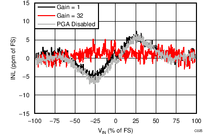
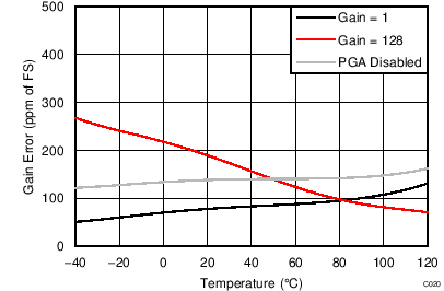
At TA = 25°C, AVDD = 3.3 V, AVSS = 0 V, and PGA enabled using external Vref = 2.5 V (unless otherwise noted).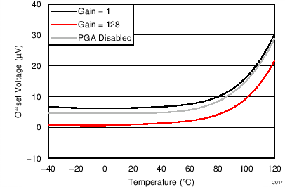
| AVDD = 3.3 V |
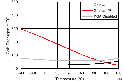
| AVDD = 3.3 V |
| AVDD = 3.3 V, external 2.5-V reference, normal mode |
Differential Input Signal
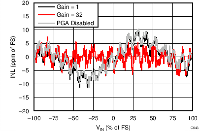
| AVDD = 3.3 V, internal reference, normal mode |
Differential Input Signal
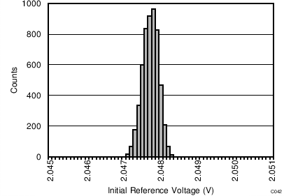
| TA = 25°C, data from 5490 devices |
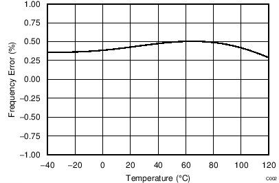
| DVDD = 3.3 V, normal mode |
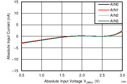
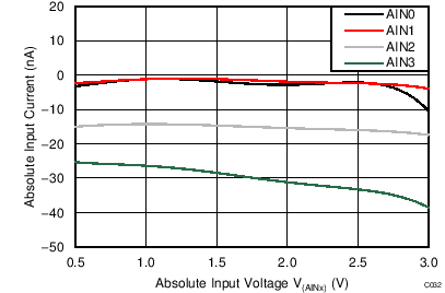
| AVDD = 3.3 V, PGA enabled, TA = –40°C |
Absolute Input Voltage
| AVDD = 3.3 V, PGA enabled, TA = 85°C |
Absolute Input Voltage
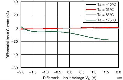
| AVDD = 3.3 V, PGA enabled, AINP = AIN0, AINN = AIN1 |
Differential Input Voltage
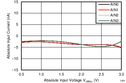
| AVDD = 3.3 V, PGA disabled, TA = –40°C |
Absolute Input Voltage
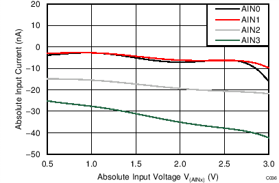
| AVDD = 3.3 V, PGA disabled, TA = 85°C |
Absolute Input Voltage
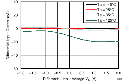
| AVDD = 3.3 V, PGA disabled, AINP = AIN0, AINN = AIN1 |
Differential Input Voltage
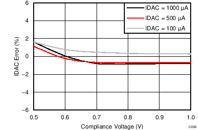
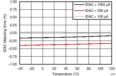
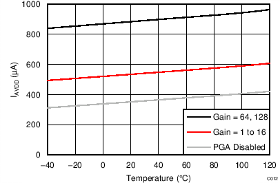
| AVDD = 3.3 V, internal reference, turbo mode |
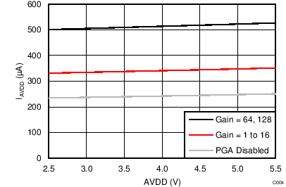
| Normal mode, internal reference |
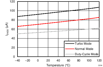
| DVDD = 3.3 V |
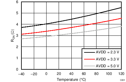
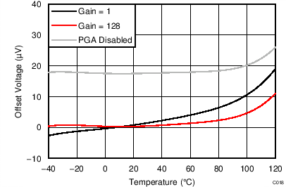
| AVDD = 5.0 V |
| AVDD = 5.0 V |
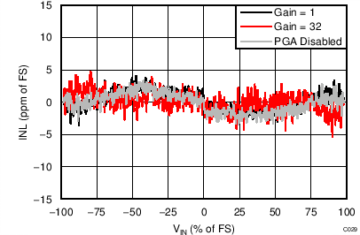
| AVDD = 5.0 V, external 2.5-V reference, normal mode |
Differential Input Signal
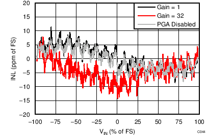
| AVDD = 5.0 V, internal reference, normal mode |
Differential Input Signal
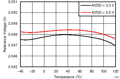
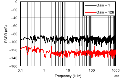
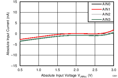
| AVDD = 3.3 V, PGA enabled, TA = 25°C |
Absolute Input Voltage
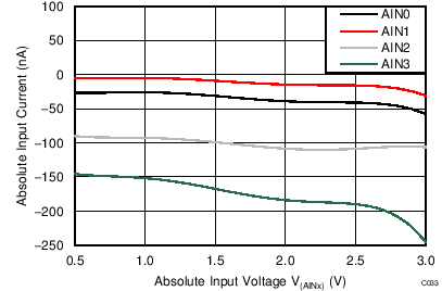
| AVDD = 3.3 V, PGA enabled, TA = 125°C |
Absolute Input Voltage
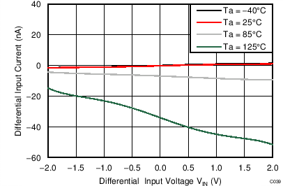
| AVDD = 3.3 V, PGA enabled, AINP = AIN3, AINN = AIN2 |
Differential Input Voltage
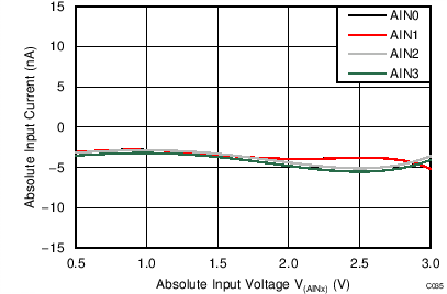
| AVDD = 3.3 V, PGA disabled, TA = 25°C |
Absolute Input Voltage
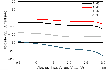
| AVDD = 3.3 V, PGA disabled, TA = 125°C |
Absolute Input Voltage
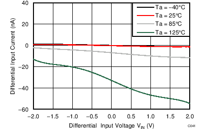
| AVDD = 3.3 V, PGA disabled, AINP = AIN3, AINN = AIN2 |
Differential Input Voltage
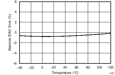
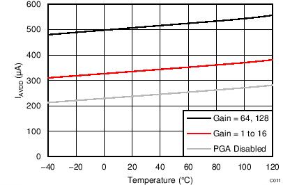
| AVDD = 3.3 V, internal reference, normal mode |
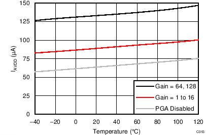
| AVDD = 3.3 V, internal reference, duty-cycle mode |
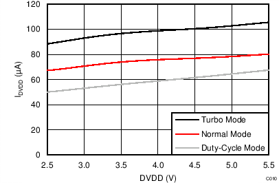
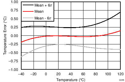
7 Parameter Measurement Information
7.1 Noise Performance
Delta-sigma (ΔΣ) analog-to-digital converters (ADCs) are based on the principle of oversampling. The input signal of a ΔΣ ADC is sampled at a high frequency (modulator frequency) and subsequently filtered and decimated in the digital domain to yield a conversion result at the respective output data rate. The ratio between modulator frequency and output data rate is called oversampling ratio (OSR). By increasing the OSR, and thus reducing the output data rate, the noise performance of the ADC can be optimized. In other words, the input-referred noise drops when reducing the output data rate because more samples of the internal modulator are averaged to yield one conversion result. Increasing the gain also reduces the input-referred noise, which is particularly useful when measuring low-level signals.
Table 1 to Table 8 summarize the device noise performance. Data are representative of typical noise performance at TA = 25°C using the internal 2.048-V reference. Data shown are the result of averaging readings from a single device over a time period of approximately 0.75 seconds and are measured with the inputs internally shorted together. Table 1, Table 3, Table 5 and Table 7 list the input-referred noise in units of μVRMS for the conditions shown. Note that µVPP values are shown in parenthesis. Table 2, Table 4, Table 6 and Table 8 list the corresponding data in effective number of bits (ENOB) calculated from μVRMS values using Equation 1. Note that noise-free bits calculated from peak-to-peak noise values using Equation 2 are shown in parenthesis.
The input-referred noise (Table 1, Table 3, Table 5 and Table 7) only changes marginally when using an external low-noise reference, such as the REF5020. To calculate ENOB numbers and noise-free bits when using a reference voltage other than 2.048 V, use Equation 1 to Equation 3:
Table 1. Noise in μVRMS (μVPP)
at AVDD = 3.3 V, AVSS = 0 V, Normal Mode, and Internal Reference = 2.048 V
| DATA RATE (SPS) |
GAIN (PGA Enabled) | |||||||
|---|---|---|---|---|---|---|---|---|
| 1 | 2 | 4 | 8 | 16 | 32 | 64 | 128 | |
| 20 | 62.50 (62.50) | 31.25 (31.25) | 15.63 (15.63) | 7.81 (7.81) | 3.91 (3.91) | 1.95 (1.95) | 0.98 (0.98) | 0.49 (0.49) |
| 45 | 62.50 (62.50) | 31.25 (31.25) | 15.63 (15.63) | 7.81 (7.81) | 3.91 (3.91) | 1.95 (1.95) | 0.98 (0.98) | 0.49 (0.51) |
| 90 | 62.50 (62.50) | 31.25 (31.25) | 15.63 (15.63) | 7.81 (7.81) | 3.91 (3.91) | 1.95 (2.14) | 0.98 (1.22) | 0.49 (0.85) |
| 175 | 62.50 (63.72) | 31.25 (34.06) | 15.63 (17.76) | 7.81 (11.20) | 3.91 (5.13) | 1.95 (3.09) | 0.98 (2.14) | 0.49 (1.60) |
| 330 | 62.50 (106.93) | 31.25 (50.78) | 15.63 (26.25) | 7.81 (14.13) | 3.91 (7.52) | 1.95 (4.66) | 0.98 (2.69) | 0.49 (1.99) |
| 600 | 62.50 (151.61) | 31.25 (72.27) | 15.63 (39.43) | 7.81 (19.26) | 3.91 (12.77) | 1.95 (6.87) | 0.98 (4.76) | 0.55 (3.34) |
| 1000 | 62.50 (227.29) | 31.25 (122.68) | 15.63 (58.53) | 7.81 (31.52) | 3.91 (18.08) | 1.95 (10.71) | 1.03 (6.52) | 0.70 (4.01) |
Table 2. ENOB from RMS Noise (Noise-free Bits from Peak-to-Peak Noise)
at AVDD = 3.3 V, AVSS = 0 V, Normal Mode, and Internal Reference = 2.048 V
| DATA RATE (SPS) |
GAIN (PGA Enabled) | |||||||
|---|---|---|---|---|---|---|---|---|
| 1 | 2 | 4 | 8 | 16 | 32 | 64 | 128 | |
| 20 | 16 (16) | 16 (16) | 16 (16) | 16 (16) | 16 (16) | 16 (16) | 16 (16) | 16 (16) |
| 45 | 16 (16) | 16 (16) | 16 (16) | 16 (16) | 16 (16) | 16 (16) | 16 (16) | 16 (15.49) |
| 90 | 16 (16) | 16 (16) | 16 (16) | 16 (16) | 16 (16) | 16 (15.87) | 16 (15.67) | 16 (15.20) |
| 175 | 16 (15.97) | 16 (15.88) | 16 (15.82) | 16 (15.48) | 16 (15.61) | 16 (15.34) | 16 (14.87) | 16 (14.29) |
| 330 | 16 (15.23) | 16 (15.30) | 16 (15.25) | 16 (15.15) | 16 (15.05) | 16 (14.74) | 16 (14.54) | 16 (13.97) |
| 600 | 16 (14.72) | 16 (14.79) | 16 (14.66) | 16 (14.70) | 16 (14.29) | 16 (14.18) | 16 (13.72) | 15.83 (13.23) |
| 1000 | 16 (14.14) | 16 (14.03) | 16 (14.09) | 16 (13.99) | 16 (13.79) | 16 (13.54) | 15.92 (13.26) | 15.49 (12.96) |
Table 3. Noise in μVRMS (μVPP) with PGA Disabled
at AVDD = 3.3 V, AVSS = 0 V, Normal Mode, and Internal Reference = 2.048 V
| DATA RATE (SPS) |
GAIN (PGA Disabled) | ||
|---|---|---|---|
| 1 | 2 | 4 | |
| 20 | 62.50 (62.50) | 31.25 (31.25) | 15.63 (15.63) |
| 45 | 62.50 (62.50) | 31.25 (31.25) | 15.63 (15.63) |
| 90 | 62.50 (62.50) | 31.25 (31.25) | 15.63 (15.63) |
| 175 | 62.50 (65.92) | 31.25 (35.40) | 15.63 (18.92) |
| 330 | 62.50 (94.24) | 31.25 (50.17) | 15.63 (28.75) |
| 600 | 62.50 (138.67) | 31.25 (78.13) | 15.63 (39.79) |
| 1000 | 62.50 (260.50) | 31.25 (120.97) | 15.63 (63.72) |
Table 4. ENOB from RMS Noise (Noise-free Bits from Peak-to-Peak Noise) with PGA Disabled
at AVDD = 3.3 V, AVSS = 0 V, Normal Mode, and Internal Reference = 2.048 V
| DATA RATE (SPS) |
GAIN (PGA Disabled) | ||
|---|---|---|---|
| 1 | 2 | 4 | |
| 20 | 16 (16) | 16 (16) | 16 (16) |
| 45 | 16 (16) | 16 (16) | 16 (16) |
| 90 | 16 (16) | 16 (16) | 16 (16) |
| 175 | 16 (15.92) | 16 (15.82) | 16 (15.72) |
| 330 | 16 (15.41) | 16 (15.32) | 16 (15.12) |
| 600 | 16 (14.85) | 16 (14.68) | 16 (14.65) |
| 1000 | 16 (13.94) | 16 (14.05) | 16 (13.97) |
Table 5. Noise in μVRMS (μVPP)
at AVDD = 3.3 V, AVSS = 0 V, Turbo Mode, and Internal Reference = 2.048 V
| DATA RATE (SPS) |
GAIN (PGA Enabled) | |||||||
|---|---|---|---|---|---|---|---|---|
| 1 | 2 | 4 | 8 | 16 | 32 | 64 | 128 | |
| 40 | 62.50 (62.50) | 31.25 (31.25) | 15.63 (15.63) | 7.81 (7.81) | 3.91 (3.91) | 1.95 (1.95) | 0.98 (0.98) | 0.49 (0.55) |
| 90 | 62.50 (62.50) | 31.25 (31.25) | 15.63 (15.63) | 7.81 (7.81) | 3.91 (3.91) | 1.95 (1.95) | 0.98 (1.13) | 0.49 (0.69) |
| 180 | 62.50 (62.50) | 31.25 (31.25) | 15.63 (15.63) | 7.81 (7.81) | 3.91 (4.82) | 1.95 (2.57) | 0.98 (1.47) | 0.49 (1.34) |
| 350 | 62.50 (84.72) | 31.25 (40.04) | 15.63 (19.04) | 7.81 (10.13) | 3.91 (6.15) | 1.95 (3.59) | 0.98 (2.29) | 0.49 (1.39) |
| 660 | 62.50 (120.36) | 31.25 (47.36) | 15.63 (27.83) | 7.81 (17.36) | 3.91 (10.21) | 1.95 (4.43) | 0.98 (3.67) | 0.49 (2.93) |
| 1200 | 62.50 (162.35) | 31.25 (85.94) | 15.63 (44.01) | 7.81 (21.55) | 3.91 (15.14) | 1.95 (7.58) | 0.98 (5.31) | 0.57 (3.51) |
| 2000 | 62.50 (265.14) | 31.25 (127.32) | 15.63 (65.43) | 7.81 (37.02) | 3.91 (18.89) | 1.95 (12.00) | 1.13 (7.60) | 0.82 (5.81) |
Table 6. ENOB from RMS Noise (Noise-Free Bits from Peak-to-Peak Noise)
at AVDD = 3.3 V, AVSS = 0 V, Turbo Mode, and Internal Reference = 2.048 V
| DATA RATE (SPS) |
GAIN (PGA Enabled) | |||||||
|---|---|---|---|---|---|---|---|---|
| 1 | 2 | 4 | 8 | 16 | 32 | 64 | 128 | |
| 40 | 16 (16) | 16 (16) | 16 (16) | 16 (16) | 16 (16) | 16 (16) | 16 (16) | 16 (15.83) |
| 90 | 16 (16) | 16 (16) | 16 (16) | 16 (16) | 16 (16) | 16 (16) | 16 (15.80) | 16 (15.49) |
| 180 | 16 (16) | 16 (16) | 16 (16) | 16 (16) | 16 (15.70) | 16 (15.60) | 16 (15.41) | 16 (14.54) |
| 350 | 16 (15.56) | 16 (15.64) | 16 (15.71) | 16 (15.62) | 16 (15.35) | 16 (15.12) | 16 (14.77) | 16 (14.49) |
| 660 | 16 (15.05) | 16 (15.40) | 16 (15.17) | 16 (14.85) | 16 (14.61) | 16 (14.82) | 16 (14.09) | 16 (13.42) |
| 1200 | 16 (14.62) | 16 (14.54) | 16 (14.51) | 16 (14.54) | 16 (14.05) | 16 (14.04) | 16 (13.56) | 15.77 (13.15) |
| 2000 | 16 (13.92) | 16 (13.97) | 16 (13.93) | 16 (13.76) | 16 (13.73) | 16 (13.38) | 15.79 (13.04) | 15.25 (12.43) |
Table 7. Noise in μVRMS (μVPP) with PGA Disabled
at AVDD = 3.3 V, AVSS = 0 V, Turbo Mode, and Internal Reference = 2.048 V
| DATA RATE (SPS) |
GAIN (PGA Disabled) | ||
|---|---|---|---|
| 1 | 2 | 4 | |
| 40 | 62.50 (62.50) | 31.25 (31.25) | 15.63 (15.63) |
| 90 | 62.50 (62.50) | 31.25 (31.25) | 15.63 (15.63) |
| 180 | 62.50 (62.50) | 31.25 (31.25) | 15.63 (15.63) |
| 350 | 62.50 (75.20) | 31.25 (34.18) | 15.63 (17.64) |
| 660 | 62.50 (111.08) | 31.25 (56.76) | 15.63 (24.47) |
| 1200 | 62.50 (176.03) | 31.25 (89.23) | 15.63 (40.95) |
| 2000 | 62.50 (250.98) | 31.25 (131.35) | 15.63 (68.18) |
Table 8. ENOB from RMS Noise (Noise-Free Bits from Peak-to-Peak Noise) with PGA Disabled
at AVDD = 3.3 V, AVSS = 0 V, Turbo Mode, and Internal Reference = 2.048 V
| DATA RATE (SPS) |
GAIN (PGA Disabled) | ||
|---|---|---|---|
| 1 | 2 | 4 | |
| 40 | 16 (16) | 16 (16) | 16 (16) |
| 90 | 16 (16) | 16 (16) | 16 (16) |
| 180 | 16 (16) | 16 (16) | 16 (16) |
| 350 | 16 (15.73) | 16 (15.87) | 16 (15.83) |
| 660 | 16 (15.17) | 16 (15.14) | 16 (15.19) |
| 1200 | 16 (14.51) | 16 (14.49) | 16 (14.61) |
| 2000 | 16 (13.99) | 16 (13.93) | 16 (13.87) |
8 Detailed Description
8.1 Overview
The ADS1120 is a small, low-power, 16-bit, ΔΣ ADC that offers many integrated features to reduce system cost and component count in applications measuring small sensor signals.
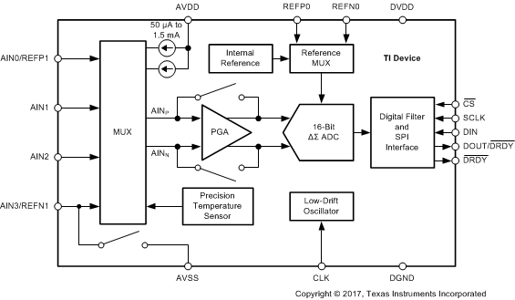
In addition to the ΔΣ ADC core and single-cycle settling digital filter, the device offers a low-noise, high input impedance, programmable gain amplifier (PGA), an internal voltage reference, and a clock oscillator. The device also integrates a highly linear and accurate temperature sensor as well as two matched programmable current sources (IDACs) for sensor excitation. All of these features are intended to reduce the required external circuitry in typical sensor applications and improve overall system performance. An additional low-side power switch eases the design of low-power bridge sensor applications. The device is fully configured through four registers and controlled by six commands through a mode 1 SPI-compatible interface. The Functional Block Diagram section shows the device functional block diagram.
The ADS1120 ADC measures a differential signal, VIN, which is the difference in voltage between nodes AINP and AINN. The converter core consists of a differential, switched-capacitor, ΔΣ modulator followed by a digital filter. The digital filter receives a high-speed bitstream from the modulator and outputs a code proportional to the input voltage. This architecture results in a very strong attenuation of any common-mode signal.
The device has two available conversion modes: single-shot and continuous conversion mode. In single-shot mode, the ADC performs one conversion of the input signal upon request and stores the value in an internal data buffer. The device then enters a low-power state to save power. Single-shot mode is intended to provide significant power savings in systems that require only periodic conversions, or when there are long idle periods between conversions. In continuous conversion mode, the ADC automatically begins a conversion of the input signal as soon as the previous conversion is completed. New data are available at the programmed data rate. Data can be read at any time without concern of data corruption and always reflect the most recently completed conversion.
8.3 Feature Description
8.3.1 Multiplexer
The device contains a very flexible input multiplexer, as shown in Figure 38. Either four single-ended signals, two differential signals, or a combination of two single-ended signals and one differential signal can be measured. The multiplexer is configured by four bits (MUX[3:0]) in the configuration register. When single-ended signals are measured, the negative ADC input (AINN) is internally connected to AVSS by a switch within the multiplexer. For system-monitoring purposes, the analog supply (AVDD – AVSS) / 4 or the currently-selected external reference voltage (V(REFPx) – V(REFNx)) / 4 can be selected as inputs to the ADC. The multiplexer also offers the possibility to route any of the two programmable current sources to any analog input (AINx) or to any dedicated reference pin (REFP0, REFN0).
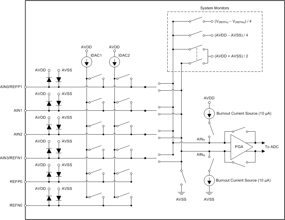 Figure 38. Analog Input Multiplexer
Electrostatic discharge (ESD) diodes to AVDD and AVSS protect the inputs. To prevent the ESD diodes from turning on, the absolute voltage on any input must stay within the range provided by Equation 4:
If the voltages on the input pins have any potential to violate these conditions, external Schottky clamp diodes or series resistors may be required to limit the input current to safe values (see the Absolute Maximum Ratings table). Overdriving an unused input on the device may affect conversions taking place on other input pins. If any overdrive on unused inputs is possible, TI recommends clamping the signal with external Schottky diodes.
8.3.2 Low-Noise PGA
The device features a low-noise, low-drift, high input impedance, programmable gain amplifier (PGA). The PGA can be set to gains of 1, 2, 4, 8, 16, 32, 64, or 128. Three bits (GAIN[2:0]) in the configuration register are used to configure the gain. A simplified diagram of the PGA is shown in Figure 39. The PGA consists of two chopper-stabilized amplifiers (A1 and A2) and a resistor feedback network that sets the PGA gain. The PGA input is equipped with an electromagnetic interference (EMI) filter.
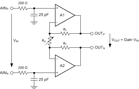 Figure 39. Simplified PGA Diagram
VIN denotes the differential input voltage VIN = (V(AINP) – V(AINN)). The gain of the PGA can be calculated with Equation 5:
Gain is changed inside the device using a variable resistor, RG. The differential full-scale input voltage range (FSR) of the PGA is defined by the gain setting and the reference voltage used, as shown in Equation 6:
Table 9 shows the corresponding full-scale ranges when using the internal 2.048-V reference.
Table 9. PGA Full-Scale Range
| GAIN SETTING | FSR |
|---|---|
| 1 | ±2.048 V |
| 2 | ±1.024 V |
| 4 | ±0.512 V |
| 8 | ±0.256 V |
| 16 | ±0.128 V |
| 32 | ±0.064 V |
| 64 | ±0.032 V |
| 128 | ±0.016 V |
8.3.2.1 PGA Common-Mode Voltage Requirements
To stay within the linear operating range of the PGA, the input signals must meet certain requirements that are discussed in this section.
The outputs of both amplifiers (A1 and A2) in Figure 39 can not swing closer to the supplies (AVSS and AVDD) than 200 mV. If the outputs OUTP and OUTN are driven to within 200 mV of the supply rails, the amplifiers saturate and consequently become nonlinear. To prevent this nonlinear operating condition the output voltages must meet Equation 7:
Translating the requirements of Equation 7 into requirements referred to the PGA inputs (AINP and AINN) is beneficial because there is no direct access to the outputs of the PGA. The PGA employs a symmetrical design, therefore the common-mode voltage at the output of the PGA can be assumed to be the same as the common-mode voltage of the input signal, as shown in Figure 40.
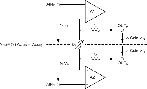 Figure 40. PGA Common-Mode Voltage
The common-mode voltage is calculated using Equation 8:
The voltages at the PGA inputs (AINP and AINN) can be expressed as Equation 9 and Equation 10:
The output voltages (V(OUTP) and V(OUTN)) can then be calculated as Equation 11 and Equation 12:
The requirements for the output voltages of amplifiers A1 and A2 (Equation 7) can now be translated into requirements for the input common-mode voltage range using Equation 11 and Equation 12, which are given in Equation 13 and Equation 14:
In order to calculate the minimum and maximum common-mode voltage limits, the maximum differential input voltage (VIN (MAX)) that occurs in the application must be used. VIN (MAX) can be less than the maximum possible FS value.
In addition to Equation 13, the minimum VCM must also meet Equation 15 because of the specific design implementation of the PGA.
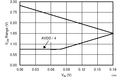
Figure 41 and Figure 42 show a graphical representation of the common-mode voltage limits for AVDD = 3.3 V and AVSS = 0 V, with gain = 1 and gain = 16, respectively.
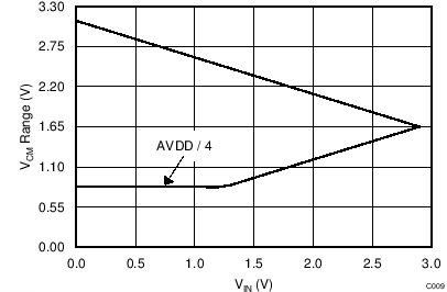
| AVDD = 3.3 V |
| AVDD = 3.3 V |
The following discussion explains how to apply Equation 13 through Equation 15 to a hypothetical application. The setup for this example is AVDD = 3.3 V, AVSS = 0 V, and gain = 16, using an external reference,
Vref = 2.5 V. The maximum possible differential input voltage VIN = (V(AINP) – V(AINN)) that can be applied is then limited to the full-scale range of FSR = ±2.5 V / 16 = ±0.156 V. Consequently, Equation 13 through Equation 15 yield an allowed VCM range of 1.45 V ≤ VCM ≤ 1.85 V.
If the sensor signal connected to the inputs in this hypothetical application does not make use of the entire full-scale range but is limited to VIN (MAX) = ±0.1 V, for example, then this reduced input signal amplitude relaxes the VCM restriction to 1.0 V ≤ VCM ≤ 2.3 V.
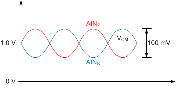
In the case of a fully-differential sensor signal, each input (AINP, AINN) can swing up to ±50 mV around the common-mode voltage (V(AINP) + V(AINN)) / 2, which must remain between the limits of 1.0 V and 2.3 V. The output of a symmetrical wheatstone bridge is an example of a fully-differential signal. Figure 43 shows a situation where the common-mode voltage of the input signal is at the lowest limit. V(OUTN) is exactly at 0.2 V in this case. Any further decrease in common-mode voltage (VCM) or increase in differential input voltage (VIN) drives V(OUTN) below 0.2 V and saturates amplifier A2.
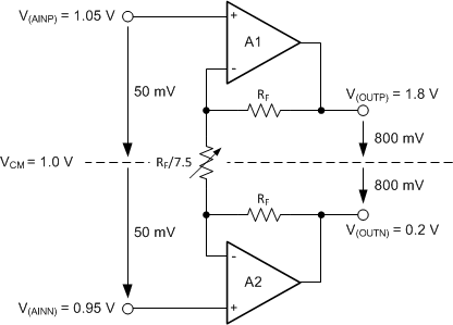 Figure 43. Example where VCM is at Lowest Limit
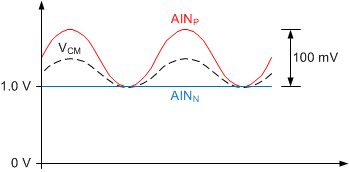
In contrast, the signal of an RTD is of a pseudo-differential nature (if implemented as shown in the RTD Measurement section), where the negative input is held at a constant voltage other than 0 V and only the voltage on the positive input changes. When a pseudo-differential signal must be measured, the negative input in this example must be biased at a voltage between 0.95 V and 2.25 V. The positive input can then swing up to
VIN (MAX) = 100 mV above the negative input. Note that in this case the common-mode voltage changes at the same time the voltage on the positive input changes. That is, while the input signal swings between 0 V ≤ VIN ≤ VIN (MAX), the common-mode voltage swings between V(AINN) ≤ VCM ≤ V(AINN) + ½ VIN (MAX). Satisfying the common-mode voltage requirements for the maximum input voltage VIN (MAX) ensures the requirements are met throughout the entire signal range.
Figure 44 and Figure 45 show examples of both fully-differential and pseudo-differential signals, respectively.
NOTE
Remember, common-mode voltage requirements with PGA enabled (Equation 13 to Equation 15) are as follows:
- VCM (MIN) ≥ AVSS + ¼ (AVDD – AVSS)
- VCM (MIN) ≥ AVSS + 0.2 V + ½ Gain · VIN (MAX)
- VCM (MAX) ≤ AVDD – 0.2 V – ½ Gain · VIN (MAX)
8.3.2.2 Bypassing the PGA
At gains of 1, 2, and 4, the device can be configured to disable and bypass the low-noise PGA by setting the PGA_BYPASS bit in the configuration register. Disabling the PGA lowers the overall power consumption and also removes the restrictions of Equation 13 through Equation 15 for the common-mode input voltage range, VCM. The usable absolute and common-mode input voltage range is (AVSS – 0.1 V ≤ V(AINx), VCM ≤ AVDD + 0.1 V) when the PGA is disabled.
In order to measure single-ended signals that are referenced to AVSS (AINP = VIN, AINN = AVSS), the PGA must be bypassed. Configure the device for single-ended measurements by either connecting one of the analog inputs to AVSS externally or by using the internal AVSS connection of the multiplexer (MUX[3:0] settings 1000 through 1011). When configuring the internal multiplexer for settings where AINN = AVSS (MUX[3:0] = 1000 through 1011) the PGA is automatically bypassed and disabled irrespective of the PGA_BYPASS setting and gain is limited to 1, 2, and 4. In case gain is set to greater than 4, the device limits gain to 4.
When the PGA is disabled, the device uses a buffered switched-capacitor stage to obtain gains of 1, 2, and 4. An internal buffer in front of the switched-capacitor stage ensures that the effect on the input loading resulting from the capacitor charging and discharging is minimal. See Figure 21 to Figure 26 for the typical values of absolute input currents (current flowing into or out of each input) and differential input currents (difference in absolute current between positive and negative input) when the PGA is disabled.
For signal sources with high output impedance, external buffering may still be necessary. Note that active buffers introduce noise and also introduce offset and gain errors. Consider all of these factors in high-accuracy applications.
8.3.3 Modulator
A ΔΣ modulator is used in the ADS1120 to convert the analog input voltage into a pulse code modulated (PCM) data stream. The modulator runs at a modulator clock frequency of f(MOD) = f(CLK) / 16 in normal and duty-cycle mode and f(MOD) = f(CLK) / 8 in turbo mode, where f(CLK) is either provided by the internal oscillator or the external clock source. Table 10 shows the modulator frequency for each operating mode using either the internal oscillator or an external clock of 4.096 MHz.
Table 10. Modulator Clock Frequency for Different Operating Modes(1)
| OPERATING MODE | f(MOD) |
|---|---|
| Duty-cycle mode | 256 kHz |
| Normal mode | 256 kHz |
| Turbo mode | 512 kHz |
8.3.4 Digital Filter
The device uses a linear-phase finite impulse response (FIR) digital filter that performs both filtering and decimation of the digital data stream coming from the modulator. The digital filter is automatically adjusted for the different data rates and always settles within a single cycle. At data rates of 5 SPS and 20 SPS, the filter can be configured to reject 50-Hz or 60-Hz line frequencies or to simultaneously reject 50 Hz and 60 Hz. Two bits (50/60[1:0]) in the configuration register are used to configure the filter accordingly. The frequency responses of the digital filter are shown in Figure 46 to Figure 59 for different output data rates using the internal oscillator or an external 4.096-MHz clock.
The filter notches and output data rate scale proportionally with the clock frequency. For example, a notch that appears at 20 Hz when using a 4.096-MHz clock appears at 10 Hz if a 2.048-MHz clock is used. Note that the internal oscillator can vary over temperature as specified in the Electrical Characteristics table. The data rate or conversion time, respectively, and filter notches consequently vary by the same amount. Consider using an external precision clock source if a digital filter notch at a specific frequency with a tighter tolerance is required.
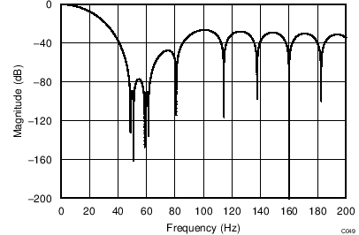
| Simultaneous 50-Hz and 60-Hz Rejection, 50/60[1:0] = 01 |
(DR = 20 SPS)
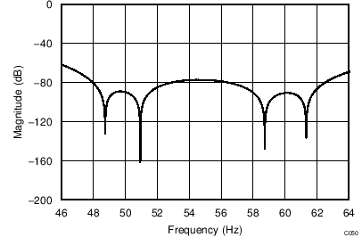
| Simultaneous 50-Hz and 60-Hz Rejection, 50/60[1:0] = 01 |
(DR = 20 SPS)
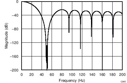
| 50-Hz Rejection Only, 50/60[1:0] = 10 |
(DR = 20 SPS)
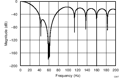
| 60-Hz Rejection Only, 50/60[1:0] = 11 |
(DR = 20 SPS)
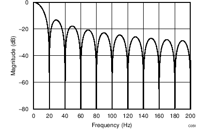
| 50/60[1:0] = 00 |
(DR = 20 SPS)
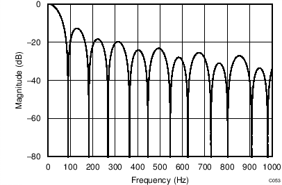
(DR = 90 SPS)
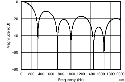
(DR = 330 SPS)
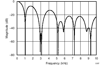
(DR = 1 kSPS)
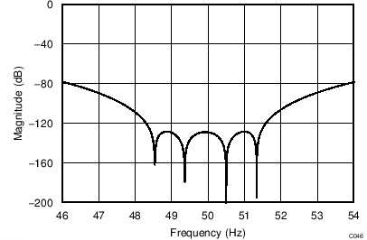
| 50-Hz Rejection Only, 50/60[1:0] = 10 |
(DR = 20 SPS)
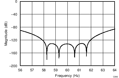
| 60-Hz Rejection Only, 50/60[1:0] = 11 |
(DR = 20 SPS)
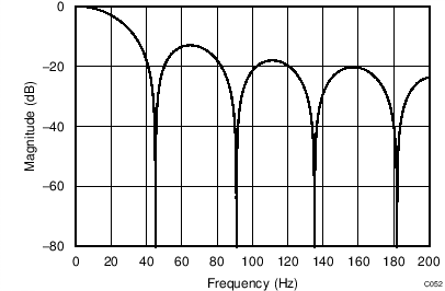
(DR = 45 SPS)
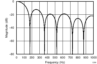
(DR = 175 SPS)
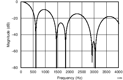
(DR = 600 SPS)
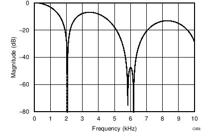
(DR = 2 kSPS)
8.3.5 Output Data Rate
Table 11 shows the actual conversion times for each data rate setting. The values provided are in terms of t(CLK) cycles using an external clock with a clock frequency of f(CLK) = 4.096 MHz. The data rates scale proportionally in case an external clock with a frequency other than 4.096 MHz is used.
Continuous conversion mode data rates are timed from one DRDY falling edge to the next DRDY falling edge. The first conversion starts 210 · t(CLK) (normal mode, duty-cycle mode) or 114 · t(CLK) (turbo mode) after the last SCLK falling edge of the START/SYNC command.
Single-shot mode data rates are timed from the last SCLK falling edge of the START/SYNC command to the DRDY falling edge and rounded to the next t(CLK). In case the internal oscillator is used, an additional oscillator wake-up time of up to 50 µs (normal mode, duty-cycle mode) or 25 µs (turbo mode) must be added in single-shot mode. The internal oscillator starts to power up at the first SCLK rising edge of the START/SYNC command. If an SCLK frequency higher than 160 kHz (normal mode, duty-cycle mode) or 320 kHz (turbo mode) is used, the oscillator may not be fully powered up at the end of the START/SYNC command. The ADC then waits until the internal oscillator is fully powered up before starting a conversion.
Single-shot conversion times in duty-cycle mode are the same as in normal mode. See the Duty-Cycle Mode section for more details on duty-cycle mode operation.
Table 11. Conversion Times
| NOMINAL DATA RATE (SPS) |
–3-dB BANDWIDTH (Hz) |
ACTUAL CONVERSION TIME (t(CLK)) | |
|---|---|---|---|
| CONTINUOUS CONVERSION MODE | SINGLE-SHOT MODE | ||
| Normal Mode | |||
| 20 | 13.1 | 204768 | 204850 |
| 45 | 20.0 | 91120 | 91218 |
| 90 | 39.6 | 46128 | 46226 |
| 175 | 77.8 | 23664 | 23762 |
| 330 | 150.1 | 12464 | 12562 |
| 600 | 279.0 | 6896 | 6994 |
| 1000 | 483.8 | 4144 | 4242 |
| Duty-Cycle Mode | |||
| 5 | 13.1 | 823120 | n/a |
| 11.25 | 20.0 | 364560 | n/a |
| 22.5 | 39.6 | 184592 | n/a |
| 44 | 77.8 | 94736 | n/a |
| 82.5 | 150.1 | 49936 | n/a |
| 150 | 279.0 | 27664 | n/a |
| 250 | 483.8 | 16656 | n/a |
| Turbo Mode | |||
| 40 | 26.2 | 102384 | 102434 |
| 90 | 39.9 | 45560 | 45618 |
| 180 | 79.2 | 23064 | 23122 |
| 350 | 155.6 | 11832 | 11890 |
| 660 | 300.3 | 6232 | 6290 |
| 1200 | 558.1 | 3448 | 3506 |
| 2000 | 967.6 | 2072 | 2130 |
Note that even though the conversion time at the 20-SPS setting is not exactly 1 / 20 Hz = 50 ms, this discrepancy does not affect the 50-Hz or 60-Hz rejection. To achieve the 50-Hz and 60-Hz rejection specified in the Electrical Characteristics, the external clock frequency must be 4.096 MHz. When using the internal oscillator, the conversion time and filter notches vary by the amount specified in the Electrical Characteristics table for oscillator accuracy.
8.3.6 Voltage Reference
The device offers an integrated low-drift, 2.048-V reference. For applications that require a different reference voltage value or a ratiometric measurement approach, the device offers two differential reference input pairs (REFP0, REFN0 and REFP1, REFN1). In addition, the analog supply (AVDD – AVSS) can be used as a reference.
The reference source is selected by two bits (VREF[1:0]) in the configuration register. By default, the internal reference is selected. The internal voltage reference requires less than 25 µs to fully settle after power-up, when coming out of power-down mode, or when switching from an external reference source to the internal reference.
The differential reference inputs allow freedom in the reference common-mode voltage. REFP0 and REFN0 are dedicated reference inputs whereas REFP1 and REFN1 are shared with inputs AIN0 and AIN3, respectively. All reference inputs are internally buffered to increase input impedance. Therefore, additional reference buffers are usually not required when using an external reference. When used in ratiometric applications, the reference inputs do not load the external circuitry. Note that the analog supply current increases when using an external reference because the reference buffers are enabled.
In most cases the conversion result is directly proportional to the stability of the reference source. Any noise and drift of the voltage reference is reflected in the conversion result.
8.3.7 Clock Source
The device system clock can either be provided by the internal low-drift oscillator or by an external clock source on the CLK input. Connect the CLK pin to DGND before power-up or reset to activate the internal oscillator. Connecting an external clock to the CLK pin at any time deactivates the internal oscillator after two rising edges on the CLK pin are detected. The device then operates on the external clock. After the ADS1120 switches to the external clock, the device can only be switched back to the internal oscillator by cycling the power supplies or by sending a RESET command.
8.3.8 Excitation Current Sources
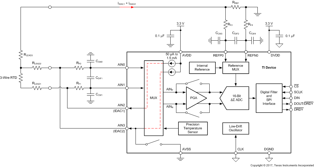
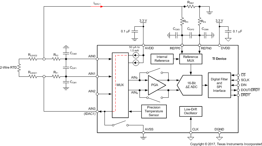
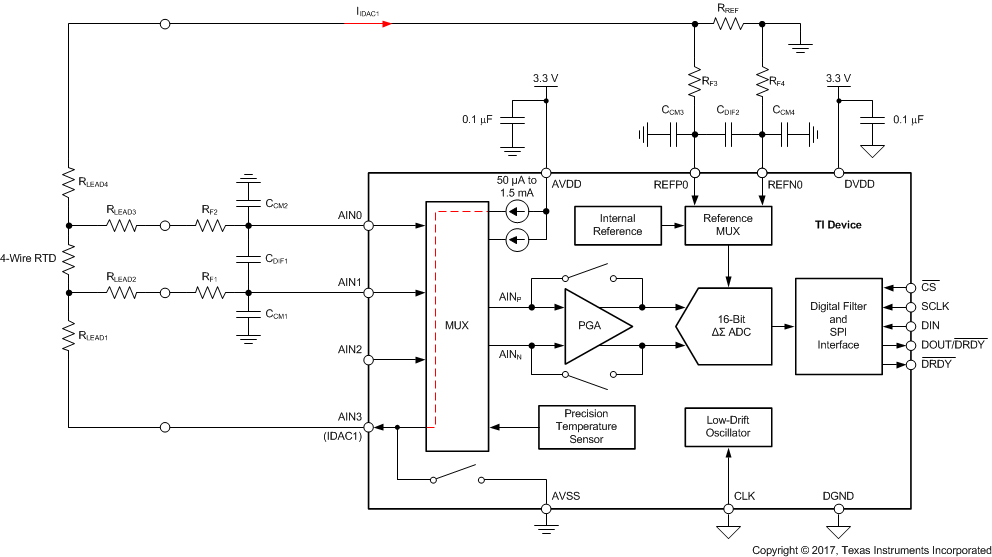
The device provides two matched programmable excitation current sources (IDACs) for RTD applications. The output current of the current sources can be programmed to 50 μA, 100 μA, 250 μA, 500 μA, 1000 μA, or 1500 μA using the respective bits (IDAC[2:0]) in the configuration register. Each current source can be connected to any of the analog inputs (AINx) as well as to any of the dedicated reference inputs (REFP0 and REFN0). Both current sources can also be connected to the same pin. Routing of the IDACs is configured by bits (I1MUX[2:0], I2MUX[2:0]) in the configuration register. Care must be taken not to exceed the compliance voltage of the IDACs. In other words, limit the voltage on the pin where the IDAC is routed to ≤ (AVDD – 0.9 V), otherwise the specified accuracy of the IDAC current is not met. For three-wire RTD applications, the matched current sources can be used to cancel errors caused by sensor lead resistance (see the 3-Wire RTD Measurement section for more details).
The IDACs require up to 200 µs to start up after the IDAC current is programmed to the respective value using bits IDAC[2:0]. If configuration registers 2 and 3 are not written during the same WREG command, TI recommends to first set the IDAC current to the respective value using bits IDAC[2:0] and thereafter select the routing for each IDAC (I1MUX[2:0], I2MUX[2:0]).
In single-shot mode, the IDACs remain active between any two conversions if the IDAC[2:0] bits are set to a value other than 000. However, the IDACs are powered down whenever the POWERDOWN command is issued.
Note that the analog supply current increases when enabling the IDACs (that is, when the IDAC[2:0] bits are set to a value other than 000). The IDAC circuit needs this bias current to operate even when the IDACs are not routed to any pin (I1MUX[2:0] = I2MUX[2:0] = 000). In addition, the selected output current is drawn from the analog supply when I1MUX[2:0] or I2MUX[2:0] are set to a value other than 000.
8.3.9 Low-Side Power Switch
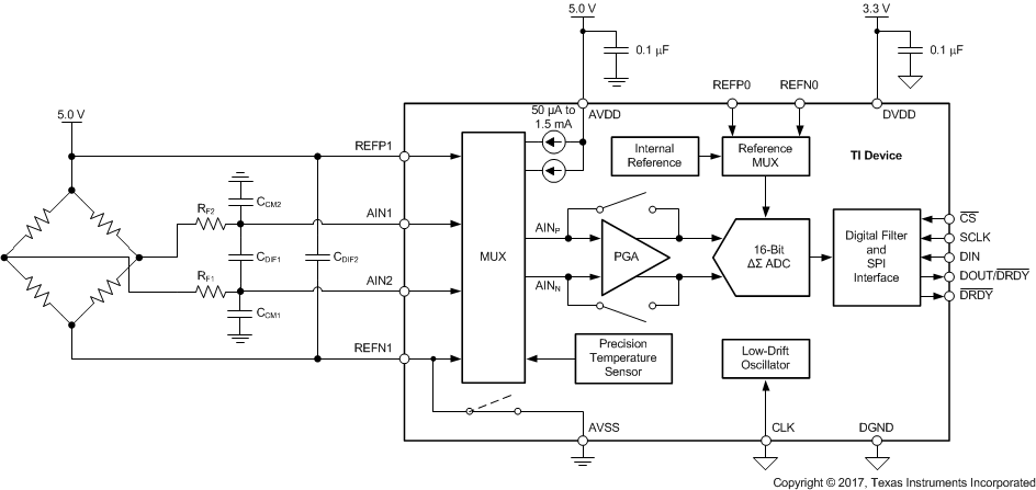
A low-side power switch with low on-resistance connected between the analog input AIN3/REFN1 and AVSS is integrated in the device as well. This power switch can be used to reduce system power consumption in bridge sensor applications by powering down the bridge circuit between conversions. When the respective bit (PSW) in the configuration register is set, the switch automatically closes when the START/SYNC command is sent and opens when the POWERDOWN command is issued. Note that the switch stays closed between conversions in single-shot mode in case the PSW bit is set to 1. The switch can be opened at any time by setting the PSW bit to 0. By default, the switch is always open.
8.3.10 Sensor Detection
To help detect a possible sensor malfunction, the device provides internal 10-µA, burn-out current sources. When enabled by setting the respective bit (BCS) in the configuration register, one current source sources current to the positive analog input (AINP) currently selected while the other current source sinks current form the selected negative analog input (AINN).
In case of an open circuit in the sensor, these burn-out current sources pull the positive input towards AVDD and the negative input towards AVSS, resulting in a full-scale reading. A full-scale reading may also indicate that the sensor is overloaded or that the reference voltage is absent. A near-zero reading may indicate a shorted sensor. Note that the absolute value of the burn-out current sources typically varies by ±10% and the internal multiplexer adds a small series resistance. Therefore, distinguishing a shorted sensor condition from a normal reading can be difficult, especially if an RC filter is used at the inputs. In other words, even if the sensor is shorted, the voltage drop across the external filter resistance and the residual resistance of the multiplexer causes the output to read a value higher than zero.
Keep in mind that ADC readings of a functional sensor may be corrupted when the burn-out current sources are enabled. TI recommends disabling the burn-out current sources when preforming the precision measurement, and only enabling them to test for sensor fault conditions.
8.3.11 System Monitor
The device provides some means for monitoring the analog power supply and the external voltage reference. To select a monitoring voltage, the internal multiplexer (MUX[3:0]) must be configured accordingly in the configuration register. The device automatically bypasses the PGA and sets the gain to 1, irrespective of the configuration register settings while the monitoring feature is used. Note that the system monitor function only provides a coarse result and is not meant to be a precision measurement.
When measuring the analog power supply (MUX[3:0] = 1101), the resulting conversion is approximately (AVDD – AVSS) / 4. The device uses the internal 2.048-V reference for the measurement regardless of what reference source is selected in the configuration register (VREF[1:0]).
When monitoring one of the two possible external reference voltage sources (MUX[3:0] = 1100), the result is approximately (V(REFPx) – V(REFNx)) / 4. REFPx and REFNx denote the external reference input pair selected in the configuration register (VREF[1:0]). The device automatically uses the internal reference for the measurement.
8.3.12 Offset Calibration
The internal multiplexer offers the option to short both PGA inputs (AINP and AINN) to mid-supply (AVDD + AVSS) / 2. This option can be used to measure and calibrate the device offset voltage by storing the result of the shorted input voltage reading in a microcontroller and consequently subtracting the result from each following reading. TI recommends taking multiple readings with the inputs shorted and averaging the result to reduce the effect of noise.
8.3.13 Temperature Sensor
The ADS1120 offers an integrated precision temperature sensor. The temperature sensor mode is enabled by setting bit TS = 1 in the configuration register. When in temperature sensor mode, the settings of configuration register 0 have no effect and the device uses the internal reference for measurement, regardless of the selected voltage reference source. Temperature readings follow the same process as the analog inputs for starting and reading conversion results. Temperature data are represented as a 14-bit result that is left-justified within the 16-bit conversion result. Data are output starting with the most significant byte (MSB). When reading the two data bytes, the first 14 bits are used to indicate the temperature measurement result. One 14-bit LSB equals 0.03125°C. Negative numbers are represented in binary twos complement format, as shown in Table 12.
Table 12. 14-Bit Temperature Data Format
| TEMPERATURE (°C) | DIGITAL OUTPUT | |
|---|---|---|
| BINARY | HEX | |
| 128 | 01 0000 0000 0000 | 1000 |
| 127.96875 | 00 1111 1111 1111 | 0FFF |
| 100 | 00 1100 1000 0000 | 0C80 |
| 75 | 00 1001 0110 0000 | 0960 |
| 50 | 00 0110 0100 0000 | 0640 |
| 25 | 00 0011 0010 0000 | 0320 |
| 0.25 | 00 0000 0000 1000 | 0008 |
| 0.03125 | 00 0000 0000 0001 | 0001 |
| 0 | 00 0000 0000 0000 | 0000 |
| –0.25 | 11 1111 1111 1000 | 3FF8 |
| –25 | 11 1100 1110 0000 | 3CE0 |
| –55 | 11 1001 0010 0000 | 3920 |
8.3.13.1 Converting from Temperature to Digital Codes
8.3.13.1.1 For Positive Temperatures (for Example, 50°C):
Twos complement is not performed on positive numbers. Therefore, simply convert the number to binary code in a 14-bit, left-justified format with the MSB = 0 to denote the positive sign.
Example: 50°C / (0.03125°C per count) = 1600 = 0640h = 00 0110 0100 0000
8.3.13.1.2 For Negative Temperatures (for Example, –25°C):
Generate the twos complement of a negative number by complementing the absolute binary number and adding 1. Then, denote the negative sign with the MSB = 1.
Example: |–25°C| / (0.03125°C per count) = 800 = 0320h = 00 0011 0010 0000
Twos complement format: 11 1100 1101 1111 + 1 = 11 1100 1110 0000
8.3.13.2 Converting from Digital Codes to Temperature
To convert from digital codes to temperature, first check whether the MSB is a 0 or a 1. If the MSB is a 0, simply multiply the decimal code by 0.03125°C to obtain the result. If the MSB = 1, subtract 1 from the result and complement all bits. Then, multiply the result by –0.03125°C.
Example: The device reads back 0960h: 0960h has an MSB = 0.
0960h · 0.03125°C = 2400 · 0.03125°C = 75°C
Example: The device reads back 3CE0h: 3CE0h has an MSB = 1.
Subtract 1 and complement the result: 3CE0h → 0320h
0320h · (–0.03125°C) = 800 · (–0.03125°C) = –25°C
8.4 Device Functional Modes
8.4.1 Power-Up and Reset
When the device powers up, a reset is performed. The reset process takes approximately 50 µs. After this power-up reset time, all internal circuitry (including the voltage reference) are stable and communication with the device is possible. As part of the reset process, the device sets all bits in the configuration registers to the respective default settings. By default, the device is set to single-shot mode. After power-up, the device performs a single conversion using the default register settings and then enters a low-power state. When the conversion is complete, the DRDY pin transitions from high to low. The high-to-low transition of the DRDY pin can be used to signal that the ADS1120 is operational and ready to use. The power-up behavior is intended to prevent systems with tight power-supply requirements from encountering a current surge during power-up.
8.4.2 Conversion Modes
The device can be operated in one of two conversion modes that can be selected by the CM bit in the configuration register. These conversion modes are single-shot and continuous conversion mode.
8.4.2.1 Single-Shot Mode
In single-shot mode, the device only performs a conversion when a START/SYNC command is issued. The device consequently performs one single conversion and returns to a low-power state afterwards. The internal oscillator and all analog circuitry (except for the excitation current sources) are turned off while the device waits in this low-power state until the next conversion is started. In addition, every write access to any configuration register also starts a new conversion. Writing to any configuration register while a conversion is ongoing functions as a new START/SYNC command that stops the current conversion and restarts a single new conversion. Each conversion is fully settled (assuming the analog input signal settles to its final value before the conversion starts) because the device digital filter settles within a single cycle.
8.4.2.2 Continuous Conversion Mode
In continuous conversion mode, the device continuously performs conversions. When a conversion completes, the device places the result in the output buffer and immediately begins another conversion.
In order to start continuous conversion mode, the CM bit must be set to 1 followed by a START/SYNC command. The first conversion starts 210 · t(CLK) (normal mode, duty-cycle mode) or 114 · t(CLK) (turbo mode) after the last SCLK falling edge of the START/SYNC command. Writing to any configuration register during an ongoing conversion restarts the current conversion. TI recommends always sending a START/SYNC command immediately after the CM bit is set to 1.
8.4.3 Operating Modes
In addition to the different conversion modes, the device can also be operated in different operating modes that can be selected to trade-off power consumption, noise performance, and output data rate. These modes are: normal mode, duty-cycle mode, turbo mode, and power-down mode.
8.4.3.1 Normal Mode
Normal mode is the default mode of operation after power-up. In this mode, the internal modulator of the ΔΣ ADC runs at a modulator clock frequency of f(MOD) = f(CLK) / 16, where the system clock (f(CLK)) is either provided by the internal oscillator or the external clock source. The modulator frequency is 256 kHz when using the internal oscillator. Normal mode offers output data rate options ranging from 20 SPS to 1 kSPS with the internal oscillator. The data rate is selected by the DR[2:0] bits in the configuration register. In case an external clock source with a clock frequency other than 4.096 MHz is used, the data rates scale accordingly. For example, using an external clock with f(CLK) = 2.048 MHz yields data rates ranging from 10 SPS to 500 SPS.
8.4.3.2 Duty-Cycle Mode
The noise performance of a ΔΣ ADC generally improves when lowering the output data rate because more samples of the internal modulator can be averaged to yield one conversion result. In applications where power consumption is critical, the improved noise performance at low data rates may not be required. For these applications, the device supports an automatic duty-cycle mode that can yield significant power savings by periodically entering a low-power state between conversions. In principle, the device runs in normal mode with a duty cycle of 25%. This functionality means the device performs one conversion in the same manner as when running in normal mode but then automatically enters a low power-state for three consecutive conversion cycles. The noise performance in duty-cycle mode is therefore comparable to the noise performance in normal mode at four times the data rate. Data rates in duty-cycle mode range from 5 SPS to 250 SPS with the internal oscillator.
8.4.3.3 Turbo Mode
Applications that require higher data rates up to 2 kSPS can operate the device in turbo mode. In this mode, the internal modulator runs at a higher frequency of f(MOD) = f(CLK) / 8. f(MOD) equals 512 kHz when the internal oscillator or an external 4.096-MHz clock is used. Note that the device power consumption increases because the modulator runs at a higher frequency. Running the ADS1120 in turbo mode at a comparable output data rate as in normal mode yields better noise performance. For example, the input-referred noise at 90 SPS in turbo mode is lower than the input-referred noise at 90 SPS in normal mode.
8.4.3.4 Power-Down Mode
When the POWERDOWN command is issued, the device enters power-down mode after completing the current conversion. In this mode, all analog circuitry (including the voltage reference and both IDACs) are powered down, the low-side power switch is opened, and the device typically only uses 400 nA of current. While in power-down mode, the device holds the configuration register settings and responds to commands, but does not perform any data conversions.
Issuing a START/SYNC command wakes up the device and either starts a single conversion or starts continuous conversion mode, depending on the conversion mode selected by the CM bit. Note that writing to any configuration register wakes up the device as well, but only starts a single conversion regardless of the selected conversion mode (CM).
8.5 Programming
8.5.1 Serial Interface
The SPI-compatible serial interface of the device is used to read conversion data, read and write the device configuration registers, and control device operation. Only SPI mode 1 (CPOL = 0, CPHA = 1) is supported. The interface consists of five control lines (CS, SCLK, DIN, DOUT/DRDY, and DRDY) but can be used with only four or even three control signals as well. The dedicated data-ready signal (DRDY) can be configured to be shared with DOUT/DRDY. If the serial bus is not shared with any other device, CS can be tied low permanently so that only signals SCLK, DIN, and DOUT/DRDY are required to communicate with the device.
8.5.1.1 Chip Select (CS)
Chip select (CS) is an active-low input that selects the device for SPI communication. This feature is useful when multiple devices share the same serial bus. CS must remain low for the duration of the serial communication. When CS is taken high, the serial interface is reset, SCLK is ignored, and DOUT/DRDY enters a high-impedance state; as such, DOUT/DRDY cannot indicate when data are ready. In situations where multiple devices are present on the bus, the dedicated DRDY pin can provide an uninterrupted monitor of the conversion status. If the serial bus is not shared with another peripheral, CS can be tied low.
8.5.1.2 Serial Clock (SCLK)
The serial clock (SCLK) features a Schmitt-triggered input and is used to clock data into and out of the device on the DIN and DOUT/DRDY pins, respectively. Even though the input has hysteresis, TI recommends keeping the SCLK signal as clean as possible to prevent glitches from accidentally shifting the data. When the serial interface is idle, hold SCLK low.
8.5.1.3 Data Ready (DRDY)
DRDY indicates when a new conversion result is ready for retrieval. When DRDY falls low, new conversion data are ready. DRDY transitions back high on the next SCLK rising edge. When no data are read during continuous conversion mode, DRDY remains low but pulses high for a duration of 2 · t(MOD) prior to the next DRDY falling edge. The DRDY pin is always actively driven, even when CS is high.
8.5.1.4 Data Input (DIN)
The data input pin (DIN) is used along with SCLK to send data (commands and register data) to the device. The device latches data on DIN on the SCLK falling edge. The device never drives the DIN pin.
8.5.1.5 Data Output and Data Ready (DOUT/DRDY)
DOUT/DRDY serves a dual-purpose function. This pin is used with SCLK to read conversion and register data from the device. Data on DOUT/DRDY are shifted out on the SCLK rising edge. DOUT/DRDY goes to a high-impedance state when CS is high.
In addition, the DOUT/DRDY pin can also be configured as a data-ready indicator by setting the DRDYM bit high in the configuration register. DOUT/DRDY then transitions low at the same time that the DRDY pin goes low to indicate new conversion data are available. Both signals can be used to detect if new data are ready. However, because DOUT/DRDY is disabled when CS is high, the recommended method of monitoring the end of a conversion when multiple devices are present on the SPI bus is to use the dedicated DRDY pin.
8.5.1.6 SPI Timeout
The ADS1120 offers an SPI timeout feature that can be used to recover communication when a serial interface transmission is interrupted. This feature is especially useful in applications where CS is permanently tied low and is not used to frame a communication sequence. Whenever a complete command is not sent within 13955 · t(MOD) (normal mode, duty-cycle mode) or 27910 · t(MOD) (turbo mode), the serial interface resets and the next SCLK pulse starts a new communication cycle. See the Modulator section for details on the modulator frequency (f(MOD) = 1 / t(MOD)) in the different operating modes. For the RREG and WREG commands, a complete command includes the command byte itself plus the register bytes that are read or written.
8.5.2 Data Format
The device provides 16 bits of data in binary twos complement format. The size of one code (LSB) is calculated using Equation 16.
A positive full-scale input [VIN ≥ (+FS – 1 LSB) = (Vref / Gain – 1 LSB)] produces an output code of 7FFFh and a negative full-scale input (VIN ≤ –FS = –Vref / Gain) produces an output code of 8000h. The output clips at these codes for signals that exceed full-scale.
Table 13 summarizes the ideal output codes for different input signals.
Table 13. Ideal Output Code versus Input Signal
| INPUT SIGNAL VIN = (V(AINP) – V(AINN)) |
IDEAL OUTPUT CODE(1) |
|---|---|
| ≥ +FS (215 – 1) / 215 | 7FFFh |
| +FS / 215 | 0001h |
| 0 | 0000h |
| –FS / 215 | FFFFh |
| ≤ –FS | 8000h |
Mapping of the analog input signal to the output codes is shown in Figure 60.
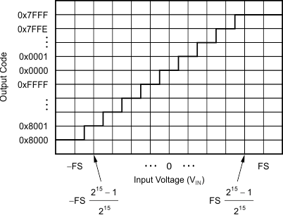 Figure 60. Code Transition Diagram
8.5.3 Commands
The device offers six different commands to control device operation, as shown in Table 14. Four commands are stand-alone instructions (RESET, START/SYNC, POWERDOWN, and RDATA). The commands to read (RREG) and write (WREG) configuration register data from and to the device require additional information as part of the instruction.
Table 14. Command Definitions
| COMMAND | DESCRIPTION | COMMAND BYTE(1) |
|---|---|---|
| RESET | Reset the device | 0000 011x |
| START/SYNC | Start or restart conversions | 0000 100x |
| POWERDOWN | Enter power-down mode | 0000 001x |
| RDATA | Read data by command | 0001 xxxx |
| RREG | Read nn registers starting at address rr | 0010 rrnn |
| WREG | Write nn registers starting at address rr | 0100 rrnn |
8.5.3.1 RESET (0000 011x)
Resets the device to the default values. Wait at least (50 µs + 32 · t(CLK)) after the RESET command is sent before sending any other command.
8.5.3.2 START/SYNC (0000 100x)
In single-shot mode, the START/SYNC command is used to start a single conversion, or (when sent during an ongoing conversion) to reset the digital filter, and then restarts a single new conversion. When the device is set to continuous conversion mode, the START/SYNC command must be issued one time to start converting continuously. Sending the START/SYNC command while converting in continuous conversion mode resets the digital filter and restarts continuous conversions.
8.5.3.3 POWERDOWN (0000 001x)
The POWERDOWN command places the device into power-down mode. This command shuts down all internal analog components, opens the low-side switch, turns off both IDACs, but holds all register values. In case the POWERDOWN command is issued while a conversion is ongoing, the conversion completes before the ADS1120 enters power-down mode. As soon as a START/SYNC command is issued, all analog components return to their previous states.
8.5.3.4 RDATA (0001 xxxx)
The RDATA command loads the output shift register with the most recent conversion result. This command can be used when DOUT/DRDY or DRDY are not monitored to indicate that a new conversion result is available. If a conversion finishes in the middle of the RDATA command byte, the state of the DRDY pin at the end of the read operation signals whether the old or the new result is loaded. If the old result is loaded, DRDY stays low, indicating that the new result is not read out. The new conversion result loads when DRDY is high.
8.5.3.5 RREG (0010 rrnn)
The RREG command reads the number of bytes specified by nn (number of bytes to be read – 1) from the device configuration register, starting at register address rr. The command is completed after nn + 1 bytes are clocked out after the RREG command byte. For example, the command to read three bytes (nn = 10) starting at configuration register 1 (rr = 01) is 0010 0110.
8.5.3.6 WREG (0100 rrnn)
The WREG command writes the number of bytes specified by nn (number of bytes to be written – 1) to the device configuration register, starting at register address rr. The command is completed after nn + 1 bytes are clocked in after the WREG command byte. For example, the command to write two bytes (nn = 01) starting at configuration register 0 (rr = 00) is 0100 0001. The configuration registers are updated on the last SCLK falling edge.
8.5.4 Reading Data
Output pins DRDY and DOUT/DRDY (if the DRDYM bit is set high in the configuration register) transition low when new data are ready for retrieval. The conversion data are written to an internal data buffer. Data can be read directly from this buffer on DOUT/DRDY when DRDY falls low without concern of data corruption. An RDATA command does not have to be sent. Data are shifted out on the SCLK rising edges, MSB first, and consist of two bytes of data.
Figure 61 to Figure 63 show the timing diagrams for reading conversion data in continuous conversion mode and single-shot mode when not using the RDATA command.
 Figure 61. Continuous Conversion Mode (DRDYM = 0)
 Figure 62. Continuous Conversion Mode (DRDYM = 1)
 Figure 63. Single-Shot Mode (DRDYM = 0)
Data can also be read at any time without synchronizing to the DRDY signal using the RDATA command. When an RDATA command is issued, the conversion result currently stored in the data buffer is shifted out on DOUT/DRDY on the following SCLK rising edges. Data can be read continuously with the RDATA command as an alternative to monitoring DRDY or DOUT/DRDY. The DRDY pin can be polled after the LSB is clocked out to determine if a new conversion result was loaded. If a new conversion completes during the read operation but data from the previous conversion are read, then DRDY is low. Otherwise, if the most recent result is read, DRDY is high. Figure 64 and Figure 65 illustrate the behavior for both cases.
 Figure 64. State of DRDY when a New Conversion Finishes During an RDATA Command
 Figure 65. State of DRDY when the Most Recent Conversion Result is Read During an RDATA Command
8.5.5 Sending Commands
The device serial interface is capable of full-duplex operation while reading conversion data when not using the RDATA command. Full-duplex operation means commands are decoded at the same time that conversion data are read. Commands can be sent on any 8-bit data boundary during a data read operation. When a RREG or RDATA command is recognized, the current data read operation is aborted and the conversion data are corrupted, unless the command is sent while the last byte of the conversion result is retrieved. The device starts to output the requested data on DOUT/DRDY at the first SCLK rising edge after the command byte. To read data without interruption, keep DIN low while clocking out data.
A WREG command can be sent without corrupting an ongoing read operation. Figure 66 shows an example for sending a WREG command to write two configuration registers while reading conversion data in continuous conversion mode. After the command is clocked in (after the 32nd SCLK falling edge), the device resets the digital filter and starts converting with the new register settings. The WREG command can be sent on any of the 8-bit boundaries.
 Figure 66. Example of Reading Data while Simultaneously Sending a WREG Command
Note that the serial interface does not decode commands while an RDATA or RREG command is executed. That is, all 16 bits of the conversion result must be read after the RDATA command is issued and all requested registers must be read after a RREG command is sent before a new command can be issued.
8.5.6 Interfacing with Multiple Devices
When connecting multiple ADS1120 devices to a single SPI bus, SCLK, DIN, and DOUT/DRDY can be safely shared by using a dedicated chip-select (CS) line for each SPI-enabled device. When CS transitions high for the respective device, DOUT/DRDY enters a 3-state mode. Therefore, DOUT/DRDY cannot be used to indicate when new data are available if CS is high, regardless of the DRDYM bit setting in the configuration register. Only the dedicated DRDY pin indicates that new data are available, because the DRDY pin is actively driven even when CS is high.
In some cases the DRDY pin cannot be interfaced to the microcontroller. This scenario can occur if there are insufficient GPIO channels available on the microcontroller or if the serial interface must be galvanically isolated and thus the amount of channels must be limited. Therefore, in order to evaluate when a new conversion of one of the devices is ready, the microcontroller can periodically drop CS to the respective device and poll the state of the DOUT/DRDY pin. When CS goes low, the DOUT/DRDY pin immediately drives either high or low, provided that the DRDYM bit is configured to 1. If the DOUT/DRDY line drives low, when CS is taken low, new data are currently available. If the DOUT/DRDY line drives high, no new data are available. This procedure requires that DOUT/DRDY is high after reading each conversion result and before taking CS high. To make sure DOUT/DRDY is taken high, send 16 additional SCLKs with DIN held low after each data read operation. DOUT/DRDY reads low during the first eight SCLKs after the conversion result is read, and reads high during the following eight SCLKs, as shown in Figure 67. Alternatively, valid data can be retrieved from the device at any time without concern of data corruption by using the RDATA command.
 Figure 67. Example of Taking DOUT/DRDY High After Reading a Conversion Result
8.6 Register Map
8.6.1 Configuration Registers
The device has four 8-bit configuration registers that are accessible through the serial interface using the RREG and WREG commands. The configuration registers control how the device operates and can be changed at any time without causing data corruption. After power-up or reset, all registers are set to the default values (which are all 0). All registers retain their values during power-down mode. Table 15 shows the register map of the configuration registers.
Table 15. Configuration Register Map
8.6.1.1 Configuration Register 0 (offset = 00h) [reset = 00h]
| 7 | 6 | 5 | 4 | 3 | 2 | 1 | 0 |
| MUX[3:0] | GAIN[2:0] | PGA_BYPASS | |||||
| R/W-0h | R/W-0h | R/W-0h | |||||
| LEGEND: R/W = Read/Write; -n = value after reset |
Table 16. Configuration Register 0 Field Descriptions
| Bit | Field | Type | Reset | Description |
|---|---|---|---|---|
| 7:4 | MUX[3:0] | R/W | 0h | Input multiplexer configuration
These bits configure the input multiplexer. For settings where AINN = AVSS, the PGA must be disabled (PGA_BYPASS = 1) and only gains 1, 2, and 4 can be used. 0000 : AINP = AIN0, AINN = AIN1 (default) 0001 : AINP = AIN0, AINN = AIN2 0010 : AINP = AIN0, AINN = AIN3 0011 : AINP = AIN1, AINN = AIN2 0100 : AINP = AIN1, AINN = AIN3 0101 : AINP = AIN2, AINN = AIN3 0110 : AINP = AIN1, AINN = AIN0 0111 : AINP = AIN3, AINN = AIN2 1000 : AINP = AIN0, AINN = AVSS 1001 : AINP = AIN1, AINN = AVSS 1010 : AINP = AIN2, AINN = AVSS 1011 : AINP = AIN3, AINN = AVSS 1100 : (V(REFPx) – V(REFNx)) / 4 monitor (PGA bypassed) 1101 : (AVDD – AVSS) / 4 monitor (PGA bypassed) 1110 : AINP and AINN shorted to (AVDD + AVSS) / 2 1111 : Reserved |
| 3:1 | GAIN[2:0] | R/W | 0h | Gain configuration
These bits configure the device gain. Gains 1, 2, and 4 can be used without the PGA. In this case, gain is obtained by a switched-capacitor structure. 000 : Gain = 1 (default) 001 : Gain = 2 010 : Gain = 4 011 : Gain = 8 100 : Gain = 16 101 : Gain = 32 110 : Gain = 64 111 : Gain = 128 |
| 0 | PGA_BYPASS | R/W | 0h | Disables and bypasses the internal low-noise PGA
Disabling the PGA reduces overall power consumption and allows the common-mode voltage range (VCM) to span from AVSS – 0.1 V to AVDD + 0.1 V. The PGA can only be disabled for gains 1, 2, and 4. The PGA is always enabled for gain settings 8 to 128, regardless of the PGA_BYPASS setting. 0 : PGA enabled (default) 1 : PGA disabled and bypassed |
8.6.1.2 Configuration Register 1 (offset = 01h) [reset = 00h]
| 7 | 6 | 5 | 4 | 3 | 2 | 1 | 0 |
| DR[2:0] | MODE[1:0] | CM | TS | BCS | |||
| R/W-0h | R/W-0h | R/W-0h | R/W-0h | R/W-0h | |||
| LEGEND: R/W = Read/Write; -n = value after reset |
Table 17. Configuration Register 1 Field Descriptions
| Bit | Field | Type | Reset | Description |
|---|---|---|---|---|
| 7:5 | DR[2:0] | R/W | 0h | Data rate
These bits control the data rate setting depending on the selected operating mode. Table 18 lists the bit settings for normal, duty-cycle, and turbo mode. |
| 4:3 | MODE[1:0] | R/W | 0h | Operating mode
These bits control the operating mode the device operates in. 00 : Normal mode (256-kHz modulator clock, default) 01 : Duty-cycle mode (internal duty cycle of 1:4) 10 : Turbo mode (512-kHz modulator clock) 11 : Reserved |
| 2 | CM | R/W | 0h | Conversion mode
This bit sets the conversion mode for the device. 0 : Single-shot mode (default) 1 : Continuous conversion mode |
| 1 | TS | R/W | 0h | Temperature sensor mode
This bit enables the internal temperature sensor and puts the device in temperature sensor mode. The settings of configuration register 0 have no effect and the device uses the internal reference for measurement when temperature sensor mode is enabled. 0 : Disables temperature sensor (default) 1 : Enables temperature sensor |
| 0 | BCS | R/W | 0h | Burn-out current sources
This bit controls the 10-µA, burn-out current sources. The burn-out current sources can be used to detect sensor faults such as wire breaks and shorted sensors. 0 : Current sources off (default) 1 : Current sources on |
Table 18. DR Bit Settings(1)
| NORMAL MODE | DUTY-CYCLE MODE | TURBO MODE |
|---|---|---|
| 000 = 20 SPS | 000 = 5 SPS | 000 = 40 SPS |
| 001 = 45 SPS | 001 = 11.25 SPS | 001 = 90 SPS |
| 010 = 90 SPS | 010 = 22.5 SPS | 010 = 180 SPS |
| 011 = 175 SPS | 011 = 44 SPS | 011 = 350 SPS |
| 100 = 330 SPS | 100 = 82.5 SPS | 100 = 660 SPS |
| 101 = 600 SPS | 101 = 150 SPS | 101 = 1200 SPS |
| 110 = 1000 SPS | 110 = 250 SPS | 110 = 2000 SPS |
| 111 = Reserved | 111 = Reserved | 111 = Reserved |
8.6.1.3 Configuration Register 2 (offset = 02h) [reset = 00h]
| 7 | 6 | 5 | 4 | 3 | 2 | 1 | 0 |
| VREF[1:0] | 50/60[1:0] | PSW | IDAC[2:0] | ||||
| R/W-0h | R/W-0h | R/W-0h | R/W-0h | ||||
| LEGEND: R/W = Read/Write; -n = value after reset |
Table 19. Configuration Register 2 Field Descriptions
8.6.1.4 Configuration Register 3 (offset = 03h) [reset = 00h]
| 7 | 6 | 5 | 4 | 3 | 2 | 1 | 0 |
| I1MUX[2:0] | I2MUX[2:0] | DRDYM | 0 | ||||
| R/W-0h | R/W-0h | R/W-0h | R/W-0h | ||||
| LEGEND: R/W = Read/Write; -n = value after reset |
Table 20. Configuration Register 3 Field Descriptions
| Bit | Field | Type | Reset | Description |
|---|---|---|---|---|
| 7:5 | I1MUX[2:0] | R/W | 0h | IDAC1 routing configuration
These bits select the channel where IDAC1 is routed to. 000 : IDAC1 disabled (default) 001 : IDAC1 connected to AIN0/REFP1 010 : IDAC1 connected to AIN1 011 : IDAC1 connected to AIN2 100 : IDAC1 connected to AIN3/REFN1 101 : IDAC1 connected to REFP0 110 : IDAC1 connected to REFN0 111 : Reserved |
| 4:2 | I2MUX[2:0] | R/W | 0h | IDAC2 routing configuration
These bits select the channel where IDAC2 is routed to. 000 : IDAC2 disabled (default) 001 : IDAC2 connected to AIN0/REFP1 010 : IDAC2 connected to AIN1 011 : IDAC2 connected to AIN2 100 : IDAC2 connected to AIN3/REFN1 101 : IDAC2 connected to REFP0 110 : IDAC2 connected to REFN0 111 : Reserved |
| 1 | DRDYM | R/W | 0h | DRDY mode
This bit controls the behavior of the DOUT/DRDY pin when new data are ready. 0 : Only the dedicated DRDY pin is used to indicate when data are ready (default) 1 : Data ready is indicated simultaneously on DOUT/DRDY and DRDY |
| 0 | Reserved | R/W | 0h | Reserved
Always write 0 |
9 Application and Implementation
NOTE
Information in the following applications sections is not part of the TI component specification, and TI does not warrant its accuracy or completeness. TI’s customers are responsible for determining suitability of components for their purposes. Customers should validate and test their design implementation to confirm system functionality.
9.1 Application Information
The ADS1120 is a precision, 16-bit, ΔΣ ADC that offers many integrated features to ease the measurement of the most common sensor types including various types of temperature and bridge sensors. Primary considerations when designing an application with the ADS1120 include analog input filtering, establishing an appropriate external reference for ratiometric measurements, and setting the common-mode input voltage for the internal PGA. Connecting and configuring the serial interface appropriately is another concern. These considerations are discussed in the following sections.
9.1.1 Serial Interface Connections
The principle serial interface connections for the ADS1120 are shown in Figure 72.
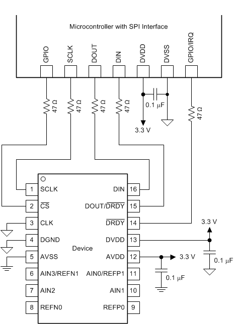 Figure 72. Serial Interface Connections
Most microcontroller SPI peripherals can operate with the ADS1120. The interface operates in SPI mode 1 where CPOL = 0 and CPHA = 1. In SPI mode 1, SCLK idles low and data are launched or changed only on SCLK rising edges; data are latched or read by the master and slave on SCLK falling edges. Details of the SPI communication protocol employed by the device can be found in the SPI Timing Requirements section.
TI recommends placing 47-Ω resistors in series with all digital input and output pins (CS, SCLK, DIN, DOUT/DRDY, and DRDY). This resistance smooths sharp transitions, suppresses overshoot, and offers some overvoltage protection. Care must be taken to meet all SPI timing requirements because the additional resistors interact with the bus capacitances present on the digital signal lines.
9.1.2 Analog Input Filtering
Analog input filtering serves two purposes: first, to limit the effect of aliasing during the sampling process and second, to reduce external noise from being a part of the measurement.
As with any sampled system, aliasing can occur if proper antialias filtering is not in place. Aliasing occurs when frequency components are present in the input signal that are higher than half the sampling frequency of the ADC (also known as the Nyquist frequency). These frequency components are folded back and show up in the actual frequency band of interest below half the sampling frequency. Note that inside a ΔΣ ADC, the input signal is sampled at the modulator frequency f(MOD) and not at the output data rate. The filter response of the digital filter repeats at multiples of the sampling frequency (f(MOD)), as shown in Figure 73. Signals or noise up to a frequency where the filter response repeats are attenuated to a certain amount by the digital filter depending on the filter architecture. Any frequency components present in the input signal around the modulator frequency or multiples thereof are not attenuated and alias back into the band of interest, unless attenuated by an external analog filter.
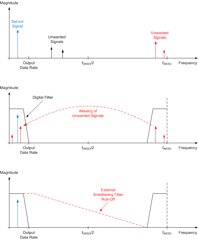 Figure 73. Effect of Aliasing
Many sensor signals are inherently bandlimited; for example, the output of a thermocouple has a limited rate of change. In this case the sensor signal does not alias back into the pass-band when using a ΔΣ ADC. However, any noise pick-up along the sensor wiring or the application circuitry can potentially alias into the pass-band. Power line-cycle frequency and harmonics are one common noise source. External noise can also be generated from electromagnetic interference (EMI) or radio frequency interference (RFI) sources, such as nearby motors and cellular phones. Another noise source typically exists on the printed circuit board (PCB) itself in the form of clocks and other digital signals. Analog input filtering helps remove unwanted signals from affecting the measurement result.
A first-order resistor-capacitor (RC) filter is (in most cases) sufficient to either totally eliminate aliasing, or to reduce the effect of aliasing to a level within the noise floor of the sensor. Ideally, any signal beyond f(MOD) / 2 is attenuated to a level below the noise floor of the ADC. The digital filter of the ADS1120 attenuates signals to a certain degree, as illustrated in the filter response plots in the Digital Filter section. In addition, noise components are usually smaller in magnitude than the actual sensor signal. Therefore, using a first-order RC filter with a cutoff frequency set at the output data rate or 10x higher is generally a good starting point for a system design.
Internal to the device, prior to the PGA inputs, is an EMI filter as shown in Figure 39. The cutoff frequency of this filter is approximately 31.8 MHz, which helps reject high-frequency interferences.
9.1.3 External Reference and Ratiometric Measurements
The full-scale range of the ADS1120 is defined by the reference voltage and the PGA gain (FSR = ±Vref / Gain). An external reference can be used instead of the integrated 2.048-V reference to adapt the FSR to the specific system needs. An external reference must be used if VIN > 2.048 V. For example, an external 5-V reference and an AVDD = 5 V are required in order to measure a single-ended signal that can swing between 0 V and 5 V.
The reference inputs of the device also allow the implementation of ratiometric measurements. In a ratiometric measurement the same excitation source that is used to excite the sensor is also used to establish the reference for the ADC. As an example, a simple form of a ratiometric measurement uses the same current source to excite both the resistive sensor element (such as an RTD) and another resistive reference element that is in series with the element being measured. The voltage that develops across the reference element is used as the reference source for the ADC. Because current noise and drift are common to both the sensor measurement and the reference, these components cancel out in the ADC transfer function. The output code is only a ratio of the sensor element and the value of the reference resistor. The value of the excitation current source itself is not part of the ADC transfer function.
9.1.4 Establishing a Proper Common-Mode Input Voltage
The ADS1120 can be used to measure various types of input signal configurations: single-ended, pseudo-differential, and fully-differential signals (which can be either unipolar or bipolar). However, configuring the device properly for the respective signal type is important.
Signals where the negative analog input is fixed and referenced to analog ground (V(AINN) = 0 V) are commonly called single-ended signals. The common-mode voltage of a single-ended signal consequently varies between 0 V and VIN / 2. If the PGA is disabled and bypassed, the common-mode input voltage of the ADS1120 can be as low as 100 mV below AVSS and as large as 100 mV above AVDD. Therefore, the PGA_BYPASS bit must be set in order to measure single-ended signals when a unipolar analog supply is used (AVSS = 0 V). Gains of 1, 2, and 4 are still possible in this configuration. Measuring a 0-mA to 20-mA or 4-mA to 20-mA signal across a load resistor of 100 Ω referenced to GND is a typical example. The ADS1120 can directly measure the signal across the load resistor using a unipolar supply, the internal 2.048-V reference, and gain = 1 when the PGA is bypassed.
If gains larger than 4 are needed to measure a single-ended signal, the PGA must be enabled. In this case, a bipolar supply is required for the ADS1120 to meet the common-mode voltage requirement of the PGA.
Signals where the negative analog input (AINN) is fixed at a voltage other the 0 V are referred to as pseudo-differential signals. The common-mode voltage of a pseudo-differential signal varies between V(AINN) and V(AINN) + VIN / 2.
Fully-differential signals in contrast are defined as signals having a constant common-mode voltage where the positive and negative analog inputs swing 180° out-of-phase but have the same amplitude.
The ADS1120 can measure pseudo-differential and fully-differential signals both with the PGA enabled or bypassed. However, the PGA must be enabled in order to use gains greater than 4. The common-mode voltage of the input signal must meet the input-common mode voltage restrictions of the PGA (as explained in the PGA Common-Mode Voltage Requirements section) when the PGA is enabled. Setting the common-mode voltage at or near (AVSS + AVDD) / 2 in most cases satisfies the PGA common-mode voltage requirements.
Signals where both the positive and negative inputs are always ≥ 0 V are called unipolar signals. These signals can in general be measured with the ADS1120 using a unipolar analog supply (AVSS = 0 V). As mentioned previously, the PGA must be bypassed in order to measure single-ended, unipolar signals when using a unipolar supply.
A signal is called bipolar when either the positive or negative input can swing below 0 V. A bipolar analog supply (such as AVDD = 2.5 V, AVSS = –2.5 V) is required in order to measure bipolar signals with the ADS1120. A typical application task is measuring a single-ended, bipolar ±10 V signal where AINN is fixed at 0 V while AINP swings between –10 V and 10 V. The ADS1120 cannot directly measure this signal because the 10 V exceeds the analog power-supply limits. However, one possible solution is to use a bipolar analog supply (AVDD = 2.5 V, AVSS = –2.5 V), gain = 1, and a resistor divider in front of the ADS1120. The resistor divider must divide the voltage down to ≤ ±2.048 V to be able to measure it using the internal 2.048-V reference.
9.1.5 Unused Inputs and Outputs
To minimize leakage currents on the analog inputs, leave unused analog and reference inputs floating, or connect the inputs to mid-supply or to AVDD. AIN3/REFN1 is an exception. Leave the AIN3/REFN1 pin floating when not used in order to avoid accidently shorting the pin to AVSS through the internal low-side switch. Connecting unused analog or reference inputs to AVSS is possible as well, but can yield higher leakage currents than the previously mentioned options.
Do not float unused digital inputs; excessive power-supply leakage current can result. Tie all unused digital inputs to the appropriate levels, DVDD or DGND, even when in power-down mode. If CS is not used, tie this pin to DGND. If the internal oscillator is used, tie the CLK pin to DGND. If the DRDY output is not used, leave the pin unconnected or tie the pin to DVDD using a weak pullup resistor.
9.1.6 Pseudo Code Example
The following list shows a pseudo code sequence with the required steps to set up the device and the microcontroller that interfaces to the ADC in order to take subsequent readings from the ADS1120 in continuous conversion mode. The dedicated DRDY pin is used to indicate availability of new conversion data. The default configuration register settings are changed to gain = 16, continuous conversion mode, and simultaneous 50-Hz and 60-Hz rejection.
| Power-up; Delay to allow power supplies to settle and power-up reset to complete; minimum of 50 µs; Configure the SPI interface of the microcontroller to SPI mode 1 (CPOL = 0, CPHA = 1); If the CS pin is not tied low permanently, configure the microcontroller GPIO connected to CS as an output; Configure the microcontroller GPIO connected to the DRDY pin as a falling edge triggered interrupt input; Set CS to the device low; Delay for a minimum of td(CSSC); Send the RESET command (06h) to make sure the device is properly reset after power-up; Delay for a minimum of 50 µs + 32 · t(CLK); Write the respective register configuration with the WREG command (43h, 08h, 04h, 10h, and 00h); As an optional sanity check, read back all configuration registers with the RREG command (23h); Send the START/SYNC command (08h) to start converting in continuous conversion mode; Delay for a minimum of td(SCCS); Clear CS to high (resets the serial interface); Loop |
|
| { Wait for DRDY to transition low; Take CS low; Delay for a minimum of td(CSSC); Send 16 SCLK rising edges to read out conversion data on DOUT/DRDY; Delay for for a minimum of td(SCCS); Clear CS to high; } |
|
| Take CS low; Delay for a minimum of td(CSSC); Send the POWERDOWN command (02h) to stop conversions and put the device in power-down mode; Delay for a minimum of td(SCCS); Clear CS to high; |
|
TI recommends running an offset calibration before performing any measurements or when changing the gain of the PGA. The internal offset of the device can, for example, be measured by shorting the inputs to mid-supply (MUX[3:1] = 1110). The microcontroller then takes multiple readings from the device with the inputs shorted and stores the average value in the microcontroller memory. When measuring the sensor signal, the microcontroller then subtracts the stored offset value from each device reading to obtain an offset compensated result. Note that the offset can be either positive or negative in value.
9.2 Typical Applications
9.2.1 K-Type Thermocouple Measurement (–200°C to +1250°C)
Figure 74 shows the basic connections of a thermocouple measurement system when using the internal high-precision temperature sensor for cold-junction compensation. Apart from the thermocouple itself, the only external circuitry required are two biasing resistors, a simple low-pass, antialiasing filter, and the power-supply decoupling capacitors.
9.2.1.1 Design Requirements
Table 21. Design Requirements
| DESIGN PARAMETER | VALUE |
|---|---|
| Supply voltage | 3.3 V |
| Reference voltage | Internal 2.048-V reference |
| Update rate | ≥10 readings per second |
| Thermocouple type | K |
| Temperature measurement range | –200°C to +1250°C |
| Measurement accuracy at TA = 25°C(1) | ±0.5°C |
offset calibration at T(TC) = T(CJ) = 25°C; no gain calibration.
9.2.1.2 Detailed Design Procedure
The biasing resistors RB1 and RB2 are used to set the common-mode voltage of the thermocouple to within the specified common-mode voltage range of the PGA (in this example, to mid-supply AVDD / 2). If the application requires the thermocouple to be biased to GND, either a bipolar supply (for example, AVDD = 2.5 V and AVSS = –2.5 V) must be used for the device to meet the common-mode voltage requirement of the PGA, or the PGA must be bypassed. When choosing the values of the biasing resistors, care must be taken so that the biasing current does not degrade measurement accuracy. The biasing current flows through the thermocouple and can cause self-heating and additional voltage drops across the thermocouple leads. Typical values for the biasing resistors range from 1 MΩ to 50 MΩ.
In addition to biasing the thermocouple, RB1 and RB2 are also useful for detecting an open thermocouple lead. When one of the thermocouple leads fails open, the biasing resistors pull the analog inputs (AIN0 and AIN1) to AVDD and AVSS, respectively. The ADC consequently reads a full-scale value, which is outside the normal measurement range of the thermocouple voltage, to indicate this failure condition.
Although the device digital filter attenuates high-frequency components of noise, TI recommends providing a first-order, passive RC filter at the inputs to further improve performance. The differential RC filter formed by RF1, RF2, and the differential capacitor CDIF offers a cutoff frequency that is calculated using Equation 17.
Two common-mode filter capacitors (CM1 and CM2) are also added to offer attenuation of high-frequency, common-mode noise components. TI recommends that the differential capacitor CDIF be at least an order of magnitude (10x) larger than the common-mode capacitors (CM1 and CM2) because mismatches in the common-mode capacitors can convert common-mode noise into differential noise.
The filter resistors RF1 and RF2 also serve as current-limiting resistors. These resistors limit the current into the analog inputs (AIN0 and AIN1) of the device to safe levels if an overvoltage on the inputs occur. Care must be taken when choosing the filter resistor values because the input currents flowing into and out of the device cause a voltage drop across the resistors. This voltage drop shows up as an additional offset error at the ADC inputs. TI recommends limiting the filter resistor values to below 1 kΩ.
The filter component values used in this design are: RF1 = RF2 = 1 kΩ, CDIF = 100 nF, and CCM1 = CCM2 = 10 nF.
The highest measurement resolution is achieved when matching the largest potential input signal to the FSR of the ADC by choosing the highest possible gain. From the design requirement, the maximum thermocouple voltage occurs at T(TC) = 1250°C and is V(TC) = 50.644 mV as defined in the tables published by the National Institute of Standards and Technology (NIST) using a cold-junction temperature of T(CJ) = 0°C. A thermocouple produces an output voltage that is proportional to the temperature difference between the thermocouple tip and the cold junction. If the cold junction is at a temperature below 0°C, the thermocouple produces a voltage larger than 50.644 mV. The isothermal block area is constrained by the operating temperature range of the device. Therefore, the isothermal block temperature is limited to –40°C. A K-type thermocouple at T(TC) = 1250°C produces an output voltage of V(TC) = 50.644 mV – (–1.527 mV) = 52.171 mV when referenced to a cold-junction temperature of T(CJ) = –40°C. The maximum gain that can be applied when using the internal 2.048-V reference is then calculated as (2.048 V / 52.171 mV) = 39.3. The next smaller PGA gain setting the device offers is 32.
The device integrates a high-precision temperature sensor that can be used to measure the temperature of the cold junction. To measure the internal temperature of the ADS1120, the device must be set to internal temperature sensor mode by setting the TS bit to 1 in the configuration register. For best performance, careful board layout is critical to achieve good thermal conductivity between the cold junction and the device package.
However, the device does not perform automatic cold-junction compensation of the thermocouple. This compensation must be done in the microcontroller that interfaces to the device. The microcontroller requests one or multiple readings of the thermocouple voltage from the device and then sets the device to internal temperature sensor mode (TS = 1) to acquire the temperature of the cold junction. An algorithm similar to the following must be implemented on the microcontroller to compensate for the cold-junction temperature:
- Measure the thermocouple voltage, V(TC), between AIN0 and AIN1.
- Measure the temperature of the cold junction, T(CJ), using the temperature sensor mode of the ADS1120.
- Convert the cold-junction temperature into an equivalent thermoelectric voltage, V(CJ), using the tables or equations provided by NIST.
- Add V(TC) and V(CJ) and translate the summation back into a thermocouple temperature using the NIST tables or equations again.
In some applications, the integrated temperature sensor of the ADS1120 cannot be used (for example, if the accuracy is not high enough or if the device cannot be placed close enough to the cold junction). The additional analog input channels of the device can be used in this case to measure the cold-junction temperature with a thermistor, RTD, or an analog temperature sensor.
The device is capable of 16-bit, noise-free resolution using a gain of 32, the internal 2.048-V reference, and a data rate of 20 SPS (see Table 1 and Table 2). Accordingly the device is able to resolve signals as small as one LSB. The LSB size is calculated using Equation 18:
To get an approximation of the achievable temperature resolution per ADC code, the LSB size is divided by the average sensitivity of a K-type thermocouple (41 µV/°C), as shown in Equation 19.
The register settings for this design are shown in Table 22.
Table 22. Register Settings
| REGISTER | SETTING | DESCRIPTION |
|---|---|---|
| 00h | 0Ah | AINP = AIN0, AINN = AIN1, gain = 32, PGA enabled |
| 01h | 04h | DR = 20 SPS, normal mode, continuous conversion mode |
| 02h | 10h | Internal voltage reference, simultaneous 50-Hz and 60-Hz rejection |
| 03h | 00h | No IDACs used |
9.2.1.3 Application Curves
Figure 75 and Figure 76 show the measurement results. The measurements are taken at TA = T(CJ) = 25°C. A system offset calibration is performed at T(TC) = 25°C, which translates to a V(TC) = 0 V when T(CJ) = 25°C. No gain calibration is implemented. The data in Figure 75 are taken using a precision voltage source as the input signal instead of a thermocouple. The respective temperature measurement error in Figure 76 is calculated from the data in Figure 75 using the NIST tables.
The design meets the required temperature measurement accuracy given in Table 21. Note that the measurement error shown in Figure 76 does not include the error of the thermocouple itself and the measurement error of the cold-junction temperature. Those two error sources are in general larger than 0.2°C and therefore, in many cases, dominate the overall system measurement accuracy.
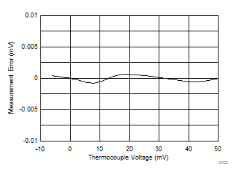
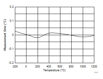
9.2.2 3-Wire RTD Measurement (–200°C to +850°C)
The ADS1120 integrates all necessary features (such as dual-matched programmable current sources, buffered reference inputs, and a PGA) to ease the implementation of ratiometric 2-, 3-, and 4-wire RTD measurements. Figure 77 shows a typical implementation of a ratiometric 3-wire RTD measurement using the excitation current sources integrated in the device to excite the RTD as well as to implement automatic RTD lead-resistance compensation.
9.2.2.1 Design Requirements
Table 23. Design Requirements
| DESIGN PARAMETER | VALUE |
|---|---|
| Supply voltage | 3.3 V |
| Update rate | 20 readings per second |
| RTD type | 3-wire Pt100 |
| Maximum RTD lead resistance | 15 Ω |
| RTD excitation current | 500 µA |
| Temperature measurement range | –200°C to +850°C |
| Measurement accuracy at TA = 25°C(1) | ±0.2°C |
offset calibration is performed with RRTD = 100 Ω; no gain calibration.
9.2.2.2 Detailed Design Procedure
The circuit in Figure 77 employs a ratiometric measurement approach. In other words, the sensor signal (that is, the voltage across the RTD in this case) and the reference voltage for the ADC are derived from the same excitation source. Therefore, errors resulting from temperature drift or noise of the excitation source cancel out because these errors are common to both the sensor signal and the reference.
In order to implement a ratiometric 3-wire RTD measurement using the device, IDAC1 is routed to one of the leads of the RTD and IDAC2 is routed to the second RTD lead. Both currents have the same value, which is programmable by the IDAC[2:0] bits in the configuration register. The design of the device ensures that both IDAC values are closely matched, even across temperature. The sum of both currents flows through a precision, low-drift reference resistor, RREF. The voltage, Vref, generated across the reference resistor (as shown in Equation 20) is used as the ADC reference voltage. Equation 20 reduces to Equation 21 because IIDAC1 = IIDAC2.
To simplify the following discussion, the individual lead resistance values of the RTD (RLEADx) are set to zero. Only IDAC1 excites the RTD to produce a voltage (VRTD) proportional to the temperature-dependable RTD value and the IDAC1 value, as shown in Equation 22.
The device internally amplifies the voltage across the RTD using the PGA and compares the resulting voltage against the reference voltage to produce a digital output code proportional to Equation 23 through Equation 25:
As can be seen from Equation 25, the output code only depends on the value of the RTD, the PGA gain, and the reference resistor (RREF), but not on the IDAC1 value. The absolute accuracy and temperature drift of the excitation current therefore does not matter. However, because the value of the reference resistor directly affects the measurement result, choosing a reference resistor with a very low temperature coefficient is important to limit errors introduced by the temperature drift of RREF.
The second IDAC2 is used to compensate for errors introduced by the voltage drop across the lead resistance of the RTD. All three leads of a 3-wire RTD typically have the same length and, thus, the same lead resistance. Also, IDAC1 and IDAC2 have the same value. Taking the lead resistance into account, the differential voltage (VIN) across the ADC inputs, AIN0 and AIN1, is calculated using Equation 26:
When RLEAD1 = RLEAD2 and IIDAC1 = IIDAC2, Equation 26 reduces to Equation 27:
In other words, the measurement error resulting from the voltage drop across the RTD lead resistance is compensated, as long as the lead resistance values and the IDAC values are well matched.
A first-order differential and common-mode RC filter (RF1, RF2, CDIF1, CCM1, and CCM2) is placed on the ADC inputs, as well as on the reference inputs (RF3, RF4, CDIF2, CCM3, and CCM4). The same guidelines for designing the input filter apply as described in the Thermocouple Measurement section. For best performance, TI recommends matching the corner frequencies of the input and reference filter. More detailed information on matching the input and reference filter can be found in application report RTD Ratiometric Measurements and Filtering Using the ADS1148 and ADS1248 (SBAA201).
The reference resistor RREF not only serves to generate the reference voltage for the device, but also sets the common-mode voltage of the RTD to within the specified common-mode voltage range of the PGA.
When designing the circuit, care must also be taken to meet the compliance voltage requirement of the IDACs. The IDACs require that the maximum voltage drop developed across the current path to AVSS be equal or less than AVDD – 0.9 V in order to operate accurately. This requirement means that Equation 28 must be met at all times.
The device also offers the possibility to route the IDACs to the same inputs used for measurement. If the filter resistor values RF1 and RF2 are small enough and well matched, IDAC1 can be routed to AIN1 and IDAC2 to AIN0 in Figure 77. In this manner, even two 3-wire RTDs sharing the same reference resistor can be measured with a single device.
This design example discusses the implementation of a 3-wire Pt100 measurement to be used to measure temperatures ranging from –200°C to +850°C as stated in Table 23. The excitation current for the Pt100 is chosen as IIDAC1 = 500 µA, which means a combined current of 1 mA is flowing through the reference resistor, RREF. As mentioned previously, besides creating the reference voltage for the ADS1120, the voltage across RREF also sets the common-mode voltage for the RTD measurement. In general, choose the largest reference voltage possible while still maintaining the compliance voltage of the IDACs as well as meeting the common-mode voltage requirement of the PGA. TI recommends setting the common-mode voltage at or near half the analog supply (in this case 3.3 V / 2 = 1.65 V), which in most cases satisfies the common-mode voltage requirements of the PGA. The value for RREF is then calculated by Equation 29:
The stability of RREF is critical to achieve good measurement accuracy over temperature and time. Choosing a reference resistor with a temperature coefficient of ±10 ppm/°C or better is advisable. If a 1.65 kΩ value is not readily available, another value near 1.65 kΩ (such as 1.62 kΩ or 1.69 kΩ) can certainly be used as well.
As a last step, the PGA gain must be selected in order to match the maximum input signal to the FSR of the ADC. The resistance of a Pt100 increases with temperature. Therefore, the maximum voltage to be measured (VIN (MAX)) occurs at the positive temperature extreme. At 850°C, a Pt100 has an equivalent resistance of approximately 391 Ω as per the NIST tables. The voltage across the Pt100 equates to Equation 30:
The maximum gain that can be applied when using a 1.65-V reference is then calculated as (1.65 V / 195.5 mV) = 8.4. The next smaller PGA gain setting available in the ADS1120 is 8. At a gain of 8, the ADS1120 offers a FSR value as described in Equation 31:
This range allows for margin with respect to initial accuracy and drift of the IDACs and reference resistor.
After selecting the values for the IDACs, RREF, and PGA gain, make sure to double check that the settings meet the common-mode voltage requirements of the PGA and the compliance voltage of the IDACs. To determine the true common-mode voltage at the ADC inputs (AIN0 and AIN1) the lead resistance must be taken into account as well.
The smallest common-mode voltage occurs at the lowest measurement temperature (–200°C) with RLEADx = 0 Ω and is calculated using Equation 32 and Equation 33.
Actually, assuming VCM (MIN) = Vref is a sufficient approximation.
VCM (MIN) must meet two requirements: Equation 15 requires VCM (MIN) to be larger than AVDD / 4 = 3.3 V / 4 = 0.825 V and Equation 13 requires VCM (MIN) to meet Equation 34:
Both restrictions are satisfied in this design with a VCM (MIN) = 1.65 V.
The largest common-mode voltage occurs at the highest measurement temperature (850°C) and is calculated using Equation 35 and Equation 36.
VCM (MAX) does meet the requirement given by Equation 14, which in this design equates to Equation 37:
Finally, the maximum voltage that can occur on input AIN1 must be calculated to determine if the compliance voltage (AVDD – 0.9 V = 3.3 V – 0.9 V = 2.4 V) of IDAC1 is met. Note that the voltage on input AIN0 is smaller than the one on input AIN1. Equation 38 and Equation 39 show that the voltage on AIN1 is less than 2.4 V, even when taking the worst-case lead resistance into account.
The register settings for this design are shown in Table 24.
Table 24. Register Settings
| REGISTER | SETTING | DESCRIPTION |
|---|---|---|
| 00h | 66h | AINP = AIN1, AINN = AIN0, gain = 8, PGA enabled |
| 01h | 04h | DR = 20 SPS, normal mode, continuous conversion mode |
| 02h | 55h | External reference (REFP0, REFN0), simultaneous 50-Hz and 60-Hz rejection, IDAC = 500 µA |
| 03h | 70h | IDAC1 = AIN2, IDAC2 = AIN3 |
9.2.2.2.1 Design Variations for 2-Wire and 4-Wire RTD Measurements
Implementing a 2- or 4-wire RTD measurement is very similar to the 3-wire RTD measurement illustrated in Figure 77, except that only one IDAC is required.
Figure 78 shows a typical circuit implementation of a 2-wire RTD measurement. The main difference compared to a 3-wire RTD measurement is with respect to the lead resistance compensation. The voltage drop across the lead resistors, RLEAD1 and RLEAD2, in this configuration is directly part of the measurement (as shown in Equation 40) because there is no means to compensate the lead resistance by use of the second current source. Any compensation must be done by calibration.
Figure 79 shows a typical circuit implementation of a 4-wire RTD measurement. Similar to the 2-wire RTD measurement, only one IDAC is required for exciting and measuring a 4-wire RTD in a ratiometric manner. The main benefit of using a 4-wire RTD is that the ADC inputs are connected to the RTD in the form of a Kelvin connection. Apart from the input leakage currents of the ADC, there is no current flow through the lead resistors RLEAD2 and RLEAD3 and therefore no voltage drop is created across them. The voltage at the ADC inputs consequently equals the voltage across the RTD and the lead resistance is of no concern.
Note that because only one IDAC is used and flows through the reference resistor, RREF, the transfer function of a 2- and 4-wire RTD measurement differs compared to the one of a 3-wire RTD measurement by a factor of 2, as shown in Equation 41.
In addition, the common-mode and reference voltage is reduced compared to the 3-wire RTD configuration. Therefore, some further modifications may be required in case the 3-wire RTD design is used to measure 2- and 4-wire RTDs as well. If the decreased common-mode voltage does not meet the VCM (MIN) requirements of the PGA anymore, either increase the value of RREF by switching in a larger resistor or, alternatively, increase the excitation current while decreasing the gain at the same time.
9.2.2.3 Application Curves
Figure 80 and Figure 81 show the measurement results. The measurements are taken at TA = 25°C. A system offset calibration is performed using a reference resistor of 100 Ω. No gain calibration is implemented. The data in Figure 80 are taken using precision resistors instead of a 3-wire Pt100. The respective temperature measurement error in Figure 81 is calculated from the data in Figure 80 using the NIST tables.
The design meets the required temperature measurement accuracy given in Table 23. Note that the measurement error shown in Figure 81 does not include the error of the RTD itself.
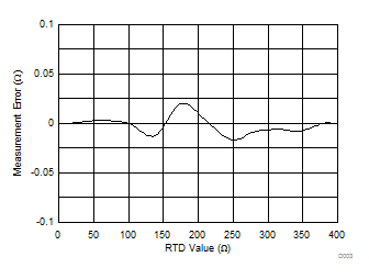
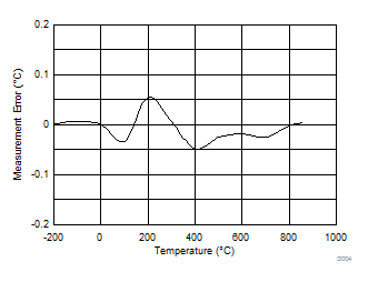
9.2.3 Resistive Bridge Measurement
The device offers several features to ease the implementation of ratiometric bridge measurements (such as a PGA with gains up to 128, buffered, differential reference inputs, and a low-side power switch).
9.2.3.1 Design Requirements
Table 25. Design Requirements
| DESIGN PARAMETER | VALUE |
|---|---|
| Analog supply voltage | 5.0 V |
| Digital supply voltage | 3.3 V |
| Load cell type | 4-wire load cell |
| Load cell sensitivity | 2 mV/V |
| Excitation voltage | 5 V |
| Noise-free counts | 8000 |
9.2.3.2 Detailed Design Procedure
To implement a ratiometric bridge measurement, the bridge excitation voltage is simultaneously used as the reference voltage for the ADC; see Figure 82. With this configuration, any drift in excitation voltage also shows up on the reference voltage, consequently canceling out drift error. Either of the two device reference input pairs can be connected to the bridge excitation voltage. However, only the negative reference input (REFN1) can be internally routed to a low-side power switch. By connecting the low side of the bridge to REFN1, the device can automatically power-down the bridge by opening the low-side power switch. When the PSW bit in the configuration register is set to 1, the device opens the switch every time a POWERDOWN command is issued and closes the switch again when a START/SYNC command is sent.
The PGA offers gains up to 128, which helps amplify the small differential bridge output signal to make optimal use of the ADC full-scale range. Using a symmetrical bridge with the excitation voltage equal to the supply voltage of the device ensures that the output signal of the bridge meets the common-mode voltage requirement of the PGA.
Note that the maximum input voltage of ADS1120 is limited to VIN (MAX) = ±[(AVDD – AVSS) – 0.4 V] / Gain, which means the entire full-scale range, FSR = ±(AVDD – AVSS) / Gain, cannot be used in this configuration. This limitation is a result of the output drive capability of the PGA amplifiers (A1 and A2); see Figure 39. The output of each amplifier must stay 200 mV away from the rails (AVDD and AVSS), otherwise the PGA becomes nonlinear. Consequently, the maximum output swing of the PGA is limited to VOUT = ±[(AVDD – AVSS) – 0.4 V].
Using a 2-mV/V load cell with a 5-V excitation yields a maximum differential output voltage of VIN (MAX) = ±10 mV, which meets Equation 42 when using a gain of 128.
A first-order differential and common-mode RC filter (RF1, RF2, CDIF1, CCM1, and CCM2) is placed on the ADC inputs. The reference has an additional capacitor CDIF2 to limit reference noise. Care must be taken to maintain a limited amount of filtering or the measurement will no longer be ratiometric.
The device is capable of 16-bit, noise-free resolution using a gain of 128 at 20 SPS for the specified reference voltage. Accordingly the device is able to resolve signals as small as one LSB. The LSB size is calculated using Equation 43:
To find the total number of counts available for the bridge measurement, the maximum output voltage is divided by the LSB value. Dividing 10 mV by 1.192 µV equates to 8389 total counts available, which meets the design parameter of 8000 counts.
The register settings for this design are shown in Table 26.
Table 26. Register Settings
| REGISTER | SETTING | DESCRIPTION |
|---|---|---|
| 00h | 3Eh | AINP = AIN1, AINN = AIN2, gain = 128, PGA enabled |
| 01h | 04h | DR = 20 SPS, normal mode, continuous conversion mode |
| 02h | 98h | External reference (REFP1, REFN1), simultaneous 50-Hz and 60-Hz rejection, PSW = 1 |
| 03h | 00h | No IDACs used |
