LP8728B-Q1 四路输出降压 DC-DC 转换器
1 特性
- LP8728B-Q1 是一款经 AECQ-100 1 级认证的汽车级产品
- 四个高效降压 DC-DC 转换器:
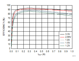
- 93% 峰值效率(VIN = 5V,VOUT = 3.3V)
- 最大输出电流 1A
- 强制脉宽调制 (PWM) 运行
- 软启动控制
- VOUT1 = 3.3V
- VOUT2 = 1.2V
- VOUT3 = 1.8V 或 2.65V(可由引脚选择)
- VOUT4 = 1.5V
- 针对每个转换器控制的独立输入使能
- 针对每个转换器的独立电源正常输出
- 输出过流和输入过压保护
- 过热保护
- 欠压闭锁 (UVLO)
2 应用
- 现场可编程门阵列 (FPGA),数字信号处理器 (DSP) 内核电源
- 移动器件的处理器电源
- 外设 I/O 电源
- 汽车安全摄像头
- 车用信息娱乐
3 说明
LP8728B-Q1 是一款四路输出电源管理单元 (PMU),针对面向汽车应用的低功耗现场可编程门阵列 (FPGA)、微处理器以及数字信号处理器 (DSP) 进行了优化。 此器件在单一封装内集成了四个高效降压 DC-DC 转换器。 每个转换器都具有高电流驱动能力以及独立控制,这使得器件能够灵活适应多类应用。 所有转换器均以 3.2MHz 固定开关频率工作于 AM 波段之上。 每个转换器的高侧开关导通时间会进行相移,以最大程度减少输入电流尖峰。
保护特性包括输出短路保护、开关电流限制、输入过压保护、输入欠压闭锁和热关断功能。 启动期间,此器件会控制输出转换率以最大限度减少输出电压过冲和输入浪涌电流。
器件信息(1)
| 器件型号 | 封装 | 封装尺寸(标称值) |
|---|---|---|
| LP8728B-Q1 | WQFN (28) | 5.00mm x 5.00mm |
- 要了解所有可用封装,请见数据表末尾的可订购产品附录。
简化电路原理图
效率
4 修订历史记录
| 日期 | 修订版本 | 注释 |
|---|---|---|
| 2015 年 2 月 | * | 最初发布。 |
5 Pin Configuration and Functions
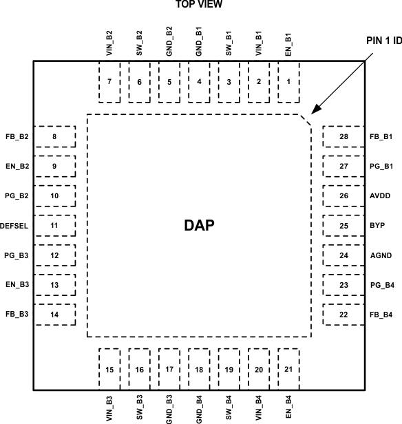
Pin Functions
| PIN | TYPE(1) | DESCRIPTION | |
|---|---|---|---|
| NUMBER | NAME | ||
| 1 | EN_B1 | D/I | Enable Buck 1 |
| 2 | VIN_B1 | P | Positive power supply input for Buck 1 |
| 3 | SW_B1 | P | Switch node for Buck 1 |
| 4 | GND_B1 | G | Power ground for Buck 1 |
| 5 | GND_B2 | G | Power ground for Buck 2 |
| 6 | SW_B2 | P | Switch node for Buck 2 |
| 7 | VIN_B2 | P | Positive power supply input for Buck 2 |
| 8 | FB_B2 | A | Feedback pin for Buck 2. Referenced against AGND. |
| 9 | EN_B2 | D/I | Enable Buck 2 |
| 10 | PG_B2 | D/O | Open-drain Power Good output for Buck 2 |
| 11 | DEFSEL | D/I | Buck 3 output voltage selection pin |
| 12 | PG_B3 | D/O | Open-drain Power Good output for Buck 3 |
| 13 | EN_B3 | D/I | Enable Buck 3 |
| 14 | FB_B3 | A | Feedback pin for Buck 3. Referenced against AGND. |
| 15 | VIN_B3 | P | Positive power supply input for Buck 3 |
| 16 | SW_B3 | P | Switch node for Buck 3 |
| 17 | GND_B3 | G | Power ground for Buck 3 |
| 18 | GND_B4 | G | Power ground for Buck 4 |
| 19 | SW_B4 | P | Switch node for Buck 4 |
| 20 | VIN_B4 | P | Positive power supply input for Buck 4 |
| 21 | EN_B4 | D/I | Enable Buck 4 |
| 22 | FB_B4 | A | Feedback pin for Buck 4. Referenced against AGND. |
| 23 | PG_B4 | D/O | Open-drain Power Good output for Buck 4 |
| 24 | AGND | G | Analog ground |
| 25 | BYP | A | Internal 1.8-V supply voltage capacitor pin. A ceramic low-ESR 1-μF capacitor should be connected from this pin to AGND. The BYP voltage is generated internally, do not supply or load this pin externally. |
| 26 | AVDD | P | Analog positive power supply pin (VIN level) |
| 27 | PG_B1 | D/O | Open-drain Power Good output for Buck 1 |
| 28 | FB_B1 | A | Feedback pin for Buck 1. Referenced against AGND. |
| DAP | Die Attachment Pad | Exposed die attachment pad should to be connected to GND plane with thermal vias to improve the thermal performance of the system. | |
6 Specifications
6.1 Absolute Maximum Ratings
over operating free-air temperature range (unless otherwise noted)(1)| MIN | MAX | UNIT | ||
|---|---|---|---|---|
| VIN | Voltage on power pins (AVDD, VIN_Bx) | –0.3 | 6 | V |
| VFB | Voltage on feedback pins (FB_Bx) | –0.3 | 6 | V |
| VSW | Voltage on buck converter switch pins (SW_Bx) | (GND_Bx – 0.2 V) to (VIN_Bx + 0.2 V) with 6 V max | V | |
| VDIG | Voltage on digital pins (PG_Bx, EN_Bx, DEFSEL) | (AGND – 0.2V) to (AVDD + 0.2 V) with 6 V max | V | |
| VBYP | Voltage on BYP pin | –0.3 | 2 | V |
| TJ(MAX) | Maximum operating junction temperature(2) | 150 | °C | |
| Maximum lead temperature (Soldering) | See(3) | |||
| Tstg | Storage temperature | –65 | 150 | °C |
6.2 ESD Ratings
| VALUE | UNIT | |||
|---|---|---|---|---|
| V(ESD) | Electrostatic discharge | Human-body model (HBM), per AEC Q100-002(1) | ±2000 | V |
| Charged-device model (CDM), per AEC Q100-011 | ±750 | |||
6.3 Recommended Operating Conditions
over operating free-air temperature range (unless otherwise noted)(1)| MIN | NOM | MAX | UNIT | ||
|---|---|---|---|---|---|
| VIN | Input voltage on AVDD, VIN_B1, VIN_B2, VIN_B3 and VIN_B4 pins | 4.5 | 5 | 5.5 | V |
| TA | Operating ambient temperature(2) | –40 | 125 | °C | |
| COUT | Effective output capacitance during operation. Min value over TA –40°C to 125°C. |
5 | 10 | 12 | µF |
| CIN | Effective input capacitance during operation. 4.5 V ≤ VIN_Bx ≤ 5.5 V. Min value over TA –40°C to 125°C. |
2.5 | 10 | µF | |
| L | Effective inductance during operation Min value over TA –40°C to 125°C. |
0.47 | 1.5 | 2 | µF |
6.4 Thermal Information
| THERMAL METRIC(1) | LP8728-Q1 | UNIT | |
|---|---|---|---|
| WQFN (RSG) | |||
| 28 PINS | |||
| RθJA | Junction-to-ambient thermal resistance(2) | 37.7 | °C/W |
| RθJCtop | Junction-to-case (top) thermal resistance | 24.5 | |
| RθJB | Junction-to-board thermal resistance | 10.8 | |
| ΨJT | Junction-to-top characterization parameter | 0.3 | |
| ΨJB | Junction-to-board characterization parameter | 10.8 | |
| RθJCbot | Junction-to-case (bottom) thermal resistance | 2.7 | |
6.5 Electrical Characteristics(1)(2)
Unless otherwise noted, VIN = 5 V, typical values apply for TA = 25°C, and minimum/maximum limits apply over junction temperature range, TJ = –40°C to 125°C.| PARAMETER | TEST CONDITIONS | MIN | TYP | MAX | UNIT | |
|---|---|---|---|---|---|---|
| ISHDN | Shutdown supply current into power connections | EN_Bx = 0 V | 1 | 6 | μA | |
| IOP | Operating current | All buck-converters active, IOUT = 0 mA | 20 | mA | ||
| LOGIC INPUTS (EN_Bx, DEFSEL) | ||||||
| VIL | Input low level | 0.4 | V | |||
| VIH | Input high level | 1.6 | V | |||
| RPD_DI | EN_Bx and DEFSEL internal pulldown resistance | 300 | 520 | 820 | kΩ | |
| TH_MIN | Minimum EN_Bx high time | 1 | ms | |||
| TL_MIN | Minimum EN_Bx low time | 10 | µs | |||
| LOGIC OUTPUTS (PG_Bx) | ||||||
| VOL | Output low level | ISINK = 3 mA | 0.4 | V | ||
| RPU | Recommended pullup resistor | 10 | kΩ | |||
| BUCK CONVERTERS | ||||||
| VOUT1 | Output voltage for Buck 1 | Fixed voltage | 3.3 | V | ||
| VOUT2 | Output voltage for Buck 2 | Fixed voltage | 1.2 | V | ||
| VOUT3 | Output voltage for Buck 3 | DEFSEL = 1 | 2.65 | V | ||
| DEFSEL = 0 | 1.8 | |||||
| VOUT4 | Output voltage for Buck 4 | Fixed voltage | 1.5 | V | ||
| VFB_Bx | Output voltage accuracy | –3% | 3% | |||
| ΔVOUT | Line regulation | 4.5 V ≤ VIN_Bx ≤ 5.5 V, ILOAD = 10 mA | 3 | mV | ||
| Load regulation | VIN = 5 V, 100 mA ≤ ILOAD ≤ 900 mA | 3 | mV | |||
| IOUT | Output current | DC load TA = 25°C |
1000 | mA | ||
| fSW | Switching frequency | 3.03 | 3.2 | 3.37 | MHz | |
| GBW | Gain bandwidth | 300 | kHz | |||
| ILIMITP | High-side switch current limit | 1200 | 1500 | 1800 | mA | |
| ILIMITN | Low-side switch current limit | Reverse current | 500 | mA | ||
| RDSONP | Pin-pin resistance for PFET | IOUT = 200 mA | 210 | 300 | mΩ | |
| RDSONN | Pin-pin resistance for NFET | IOUT = 200 mA | 140 | 240 | mΩ | |
| ILK_SW | Switch pin leakage current | VOUT = 1.8V | 1 | µA | ||
| RPD_FB | Pulldown resistor from FB_Bx pin to GND | Only active when converter disabled. All limits apply for TA = 25°C |
40 | 70 | 100 | Ω |
| KRAMP | Slew rate control | DEFSEL from 0 to 1 | 10 | mV/µs | ||
| TSTART | Start-up time | Time from first EN_Bx high to start of switching | 420 | µs | ||
| KSTART | Soft-start VOUT slew rate | 18 | mV/µs | |||
| VOLTAGE MONITORING | ||||||
| VPG | Power good threshold voltage | Power good threshold for voltage rising | 93.5% | 96% | 98% | |
| Power good threshold for voltage falling | 91% | 93% | 95% | |||
| VOVP | Input overvoltage protection trigger point | Voltage monitored on AVDD Pin, voltage rising | 5.5 | 5.7 | 5.9 | V |
| Hysteresis | 80 | mV | ||||
| VUVLO | Input undervoltage lockout (UVLO) threshold. | Voltage monitored on AVDD Pin, voltage falling | 2.7 | V | ||
| Hysteresis | 80 | mV | ||||
| THERMAL SHUTDOWN AND MONITORING | ||||||
| TSD | Thermal shutdown | Threshold, temperature rising | 150 | °C | ||
| Hysteresis | 20 | |||||
6.6 System Characteristics(1)(2)(3)
Typical values apply for TA = 25°C. Unless otherwise noted, VIN = 5 V.| PARAMETER | TEST CONDITIONS | MIN | TYP | MAX | UNIT | |
|---|---|---|---|---|---|---|
| ΔVOUT | Load transient response | IOUT 10% max load → 90% max load, 1-µs load step | 70 | mV | ||
| IOUT 90% max load → 10% max load, 1-µs load step | 70 | mV | ||||
| Line transient response | VIN_Bx stepping 4.5 V ↔ 5.5 V, tRISE = tFALL = 10 µs, IOUT = 400 mA | 20 | mV | |||
| VRIPPLE | Output voltage ripple | COUT ESR = 10 mΩ, IOUT = 200 mA | 10 | mVPP | ||
| η | Efficiency | VOUT = 3.3 V, IOUT = 300 mA | 94% | |||
| VOUT = 2.65 V, IOUT = 300 mA | 92% | |||||
| VOUT = 1.8 V, IOUT = 300 mA | 89% | |||||
| VOUT = 1.5 V, IOUT = 300 mA | 87% | |||||
| VOUT = 1.2 V, IOUT = 300 mA | 85% | |||||
6.7 Typical Characteristics
Unless otherwise noted, VIN = 5 V, TA = 25°C, inductor type: TOKO MDT2520-CN1R5M, input and output capacitor type: MuRata GRM21BR71A106KE51L.


(All Bucks Active)
7 Detailed Description
7.1 Overview
The LP8728B-Q1 has four integrated high-efficiency buck converters. Each buck converter has individual enable input and power good output pins. When the first enable pin is pulled high there is a 420-µs start-up delay when the device wakes up from the shutdown mode and all internal reference blocks are started up. Once reference blocks have settled, the corresponding buck converter turns on. Buck cores utilize the soft-start feature to limit the inrush current during start-up. Once a buck output reaches 96% (typical) of the desired output voltage, the power-good pin is pulled high (see Figure 9). When at least one buck core is active, the remaining buck converters will start up without any start-up delay.
If the output voltage drops below 93% (typical) of desired voltage due to, for example, an overload condition, the corresponding power-good pin is pulled low. The power-good signal is always held low for at least 50 ms. When the enable pin is pulled low, the corresponding buck converter's power good signals are set low, and the buck converter is instantly shut down. An output capacitor is then discharged through an internal 70-Ω (typical) pulldown resistor. The pulldown resistor is connected between buck feedback pin and ground and is only active when the enable pin is set low. When all enable signals are pulled low, the LP8728B-Q1 enters a low current shutdown mode.
7.2 Functional Block Diagram
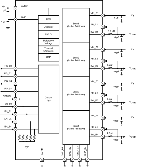
7.3 Feature Description
7.3.1 Buck Information
The buck converters are operated in a forced PWM mode. Even with light load a minimum switching pulse is generated with every switching cycle. Each buck converter's high-side switch turn-on time is phase shifted to minimize the input current ripple (see Figure 20).
7.3.1.1 Features
The following features are supported for all converters:
- Synchronous rectification
- Current mode feedback loop with PI compensator
- Forced PWM operation
- Soft start
- Power-good output
- Overvoltage comparator
In addition to the aforementioned features, Buck3 output voltage can be selected with the DEFSEL pin. If the DEFSEL pin is pulled low, VOUT3 is set to 1.8 V. If DEFSEL is pulled high, VOUT3 is set to 2.65 V.
 Figure 9. Buck Converter Start-up And Shutdown
7.3.2 Thermal Shutdown (TSD)
Thermal shutdown function shuts down all buck regulators if the device's junction temperature TJ rises above 150°C (typ.). All power-good signals are pulled low 5 ms before the buck regulators are shut down. Once TJ falls below 130°C (typical), the LP8728 will automatically start up the buck regulators. There is a 2-second safety delay included in the restart function. Buck regulators are not restarted until 2 seconds have elapsed after TJ falls below 130°C (typical). To minimize the inrush current during restarting, regulators are started in a Buck1 → Buck2 → Buck3 → Buck4 sequence. A 500-µs delay is included between each buck start-up.
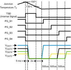 Figure 10. TSD Timing Diagram
7.3.3 Undervoltage Lockout (UVLO)
If input voltage drops below 2.7 V (typ.) the PG_Bx pins are pulled low and the buck converters are shut down. (Figure 11). The PG_Bx pins are always held low for at least 50 ms. The buck converters are restarted once the input voltage rises above UVLO level.
If a UVLO condition has lasted less than 50 ms, the PG_Bx pins are released high once 50 ms has elapsed and corresponding output voltage has settled. If an overvoltage condition has lasted more than 50 ms, the PG_Bx pins are released high once corresponding output voltage has settled.
Regulators are always restarted in a Buck1 → Buck2 → Buck3 → Buck4 sequence. A 500-µs delay is included between each buck start-up.
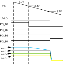 Figure 11. UVLO Operation
7.3.4 Overvoltage Protection (OVP)
Overvoltage protection protects the device in case of an overvoltage condition. If input voltage exceeds 5.7 V (typical), all PG_Bx pins are pulled low. the PG_Bx pins are always held low for at least 50 ms. Once the PG_Bx pins are pulled low, the system has 5 ms time to power down. After an overvoltage condition has lasted for 5 ms, all buck converters are shut down. The buck converters are restarted once input voltage falls below 5.62 V (typical). The buck converters are started in a Buck1 → Buck2 → Buck3 → Buck4 sequence. A 500-µs delay is included between each buck start-up.
If an overvoltage condition lasted more than 5 ms, but less than 50 ms, the PG_Bx pins are released high once 50 ms has elapsed and the corresponding output voltage has settled (Figure 12).
 Figure 12. OVP Duration Less Than 50 ms
If an overvoltage condition has lasted more than 50 ms, the power-good signals are released high once the corresponding output voltage has settled. Regulators are started in a buck1 → buck2 → buck3 → buck4 sequence. A 500-µs delay is included between each buck start-up (Figure 13). If an overvoltage condition has lasted less than 5 ms, the buck converters are not shut down. Even in this case the PG_Bx pins are held low for 50 ms.
NOTE
Since the regulators are allowed to operate for 5 ms during overvoltage condition it is the system designer’s responsibility to verify that input voltage doesn’t exceed limits stated in Absolute Maximum Ratings. Exceeding these limits may cause permanent damage to the device.
 Figure 13. OVP Duration More Than 50 ms
7.4 Device Functional Modes
7.4.1 Shutdown Mode
When all EN_Bx inputs are low, the device is in a Shutdown mode. This is a low-power mode when all buck-regulators and all internal blocks are disabled.
7.4.2 Active Mode
When the first enable pin is pulled high there is a 420-µs start-up delay when the device wakes up from the Shutdown; mode and all internal reference blocks are started up. Once the reference blocks have settled, the corresponding buck converter turns on. Buck cores utilize the soft-start feature to limit the inrush current during start-up. Once a buck output reaches 96% (typical) of the desired output voltage, the power-good pin is pulled high. When at least one buck converter is active device is in a Active mode. When device is in Active mode, the remaining buck converters will start up without any start-up delay when EN_Bx pin is pulled high. When EN_Bx pin is set low the corresponding buck converter will shut down. When all EN_Bx pins are set low the device shuts down all internal reference blocks and enters Shutdown mode.
If output voltage of a buck regulator falls below 93% (typical) of desired voltage due to, for example, an overload condition, the corresponding power good pin is pulled low. Once the output voltage rises back above 96% (typical) of desired voltage power good pin is set back high. Power good signal is held low for at least 50 ms.
If OVP, or TSD fault occurs during normal operation, all power good pins are pulled low. Once fault condition has lasted for 5 ms all buck converters are shut down. In case of UVLO fault buck regulators are instantly shut down. Once fault condition has ended buck converters are restarted in a Buck1 → Buck2 → Buck3 → Buck4 power-up sequence. A 500-µs delay is included between each buck start-up. In case of TSD fault there is a 2-second safety delay before power-up sequence.
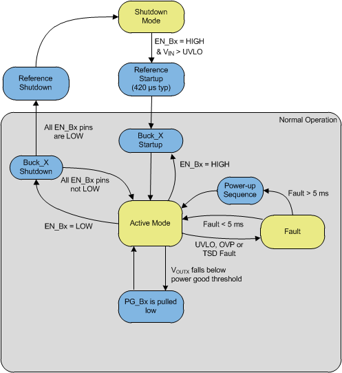 Figure 14. Device Functional Modes
8 Application and Implementation
NOTE
Information in the following applications sections is not part of the TI component specification, and TI does not warrant its accuracy or completeness. TI’s customers are responsible for determining suitability of components for their purposes. Customers should validate and test their design implementation to confirm system functionality.
8.1 Application Information
The LP8728B-Q1 is a quad-output Power Management Unit (PMU), optimized for low-power FPGAs, microprocessors, and DSPs.
8.2 Typical Application
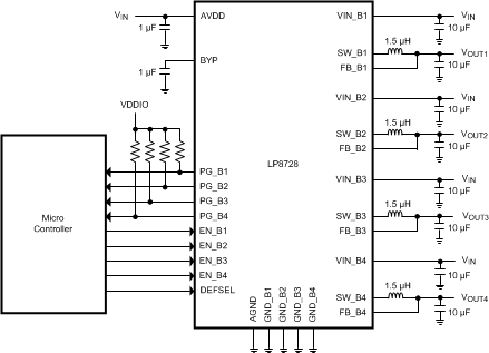
Figure 15 shows an example of a typical application. A microcontroller controls each buck converter with separate enable signals. All four power good signals are connected to a microcontroller with dedicated pullup resistors. If only one master power good signal is required all power good signals can be connected in parallel and pulled up with a single pullup resistor. VOUT3 output voltage can be selected with a DEFSEL input. If VOUT3 output voltage control is not required during operation, output voltage can be selected by connecting DEFSEL pin to VDDIO or to GND.
 Figure 15. LP8728B-Q1 Typical Application Schematic
8.2.1 Design Requirements
| DESIGN PARAMETER | EXAMPLE VALUE |
|---|---|
| Input voltage range (VIN) | 4.5 V to 5.5 V |
| Buck converter output current | 1 A maximum |
| Buck converter input capacitance | 10 µF, 6.3 V |
| Buck converter output capacitance | 10 µF, 6.3 V |
| Buck converter inductor | 1.5 µH, 1.5 A |
| AVDD pin bypass capacitor | 1 µF, 6.3 V |
| BYP pin bypass capacitor | 1 µF, 6.3 V |
8.2.2 Detailed Design Procedure
8.2.2.1 Inductor
The four converters operate with 1.5-µH inductors. The inductor has to be selected based on the DC resistance and saturation current. The DC resistance of the inductor directly effects the efficiency of the converter. Therefore, an inductor with the lowest possible DC resistance should be selected for good efficiency. The inductor should have a saturation current rating equal or higher than the high-side switch current limit (1500 mA). To minimize radiated noise shielded inductor should be used. The inductor should be placed as close to the LP8728B-Q1 as possible, and the trace from the inductor to the buck converter switch pin needs to be wide enough to withstand the high switching currents.
8.2.2.2 Input and Output Capacitors
Because buck converters have a discontinuous input current, a low equivalent series resistance (ESR) input capacitor is required for the best input-voltage filtering and to minimize interference with other circuits caused by high input voltage spikes. Each DC-DC converter requires a 10-µF ceramic input capacitor on its input pin VIN_Bx. The input capacitor capacitance can be increased without any limit for better input voltage filtering. Voltage rating of the capacitors should be at least 10V. A small 100-nF capacitor can be used in parallel to minimize high-frequency interferences. Input capacitors should be placed as close to the VIN_Bx pins as possible. Routing from input capacitor to VIN_Bx pins should be done on top layer without using any vias.
An output capacitor with a typical value of 10 µF is recommended for each converter. Ceramic capacitors with low ESR value have lowest output voltage ripple and are recommended.
Some ceramic capacitors, especially those in small packages, exhibit a strong capacitance reduction with the increased applied DC voltage (DC bias effect). The capacitance value can fall below half of the nominal capacitance. This needs to be taken into consideration and, if necessary, use a capacitor with higher value or higher voltage rating.
Table 1. Recommended External Components
| COMPONENT | DESCRIPTION | VALUE | TYPE | EXAMPLE |
|---|---|---|---|---|
| CIN_B1,2,3,4 | Buck regulator input capacitor | 10 µF | Ceramic, 10 V, X7R | MuRata, GRM21BR71A106KE51L |
| COUT_B1,2,3,4 | Buck regulator output capacitor | 10 µF | Ceramic, 10 V, X7R | MuRata, GRM21BR71A106KE51L |
| CAVDD | AVDD pin input capacitor | 1 µF | Ceramic, 10 V, X7R | MuRata, GRM188R71A105KA61D |
| CBYP | Internal LDO bypass capacitor | 1 µF | Ceramic, 10 V, X7R | MuRata, GRM188R71A105KA61D |
| LSW1,2,3 4 | Buck regulator inductor | 1.5 µH | ISAT >1.5 A, DCR < 100 mΩ | TOKO MDT2520-CN1R5M |
8.2.3 Application Performance Plots
Unless otherwise noted, VIN = 5 V, TA = 25°C, inductor type: TOKO MDT2520-CN1R5M, input and output capacitor type: MuRata GRM21BR71A106KE51L.

| IOUT from 0 mA to 1A, tRISE = tFALL = 1 µs | ||


| VIN from 4.5 V To 5.5 V, tRISE = tFALL = 10 µs | ||
9 Power Supply Recommendations
The LP8728B-Q1 is designed to operate from an input voltage supply range between 4.5 V and 5.5 V. This input supply must be well regulated and capable to supply the required input current. If the input supply is located far from the device, additional bulk capacitance may be required in addition to the ceramic bypass capacitors.