-
具有电源路径管理功能的 bq2425x 2A 单输入 I2C 独立开关模式锂离子电池充电器
- 1 特性
- 2 应用
- 3 说明
- 4 修订历史记录
- 5 说明 (续)
- 6 Device Options
- 7 Pin Configuration and Functions
- 8 Specifications
-
9 Detailed Description
- 9.1 Overview
- 9.2 Functional Block Diagram
- 9.3
Feature Description
- 9.3.1 Charge Profile
- 9.3.2 EN1 and EN2 Pins
- 9.3.3 External Settings: ISET, ILIM and VIN_DPM
- 9.3.4 BC1.2 D+/D- Detection
- 9.3.5 Transient Response
- 9.3.6 AnyBoot Battery Detection
- 9.3.7 Input Voltage Based DPM
- 9.3.8 Sleep Mode
- 9.3.9 Input Over-Voltage Protection
- 9.3.10 NTC Monitor
- 9.3.11 Production Test Mode
- 9.3.12 Safety Timer
- 9.3.13 Watchdog Timer
- 9.3.14 Fault Modes
- 9.3.15 Dynamic Power Path Management
- 9.4 Device Functional Modes
- 9.5 Programming
- 9.6 Register Maps
- 10Application and Implementation
- 11Power Supply Recommendations
- 12Layout
- 13器件和文档支持
- 14机械、封装和可订购信息
- 重要声明
具有电源路径管理功能的 bq2425x 2A 单输入 I2C 独立开关模式锂离子电池充电器
1 特性
- 具有独立电源路径的高效开关模式充电器
- 从深度放电电池或者在缺少电池的情况下启动系统
- USB 充电兼容
- 100mA、500mA、900mA、1.5A 和 2A
可选输入电流限制
- 100mA、500mA、900mA、1.5A 和 2A
- BC1.2 兼容 D+、D– 检测
- 在主机模式下(在 I2C 通信开始之后、看门狗计时器超时之前)
- 可编程电池充电电压 (VBATREG)
- 可编程充电电流 (ICHG)
- 可编程输入电流限值 (ILIM)
- 基于输入电压的可编程动态电源管理阈值 (VIN_DPM)
- 可编程输入过压保护阈值 (VOVP)
- 可编程安全计时器
- 针对以下各项的电阻器可编程默认值:
- 具有电流监控输出的高达 2A 的 ICHG (ISET)
- 具有电流监控输出的高达 2A 的 ILIM (ILIM)
- VIN_DPM (VDPM)
- 看门狗计时器禁用位
- 集成 4.9V、50mA LDO
- 完整的系统级保护
- 输入 UVLO、输入过压保护 (OVP)、电池 OVP、睡眠模式、VIN_DPM
- 输入电流限制
- 充电电流限制
- 热调节
- 热关断
- 符合 JEITA 标准的基于电压的 NTC 监控输入
- 安全计时器
- 22V 绝对最大输入电压额定值
- 10.5V 最大运行输入电压
- 用于实现高达 2A 的充电速度的低 RDS(on) 集成功率 FET
- 开漏状态输出
- 可支持小型电感器的运行频率为 3MHz 的同步固定频率 PWM 控制器
- AnyBoot 可靠电池检测算法
- 用于在任一给定充电电流上缩短充电时间的充电时间优化器
- 2.40mm x 2.00mm 30 焊球 DSBGA 和 4mm x 4mm 24 引脚 QFN 封装
2 应用
- 手机和智能手机
- MP3 播放器
- 便携式媒体播放器
- 手持设备
3 说明
bq24251 和 bq24253 是高度集成的单节锂离子电池充电器和系统电源路径管理器件,适用于采用高容量电池的空间受限型便携式 应用 。单节电池充电器具有一个由 USB 端口或交流壁式适配器供电的单一输入,用于提供多用途解决方案。
器件信息(1)
| 器件型号 | 封装 | 封装尺寸(标称值) |
|---|---|---|
| bq24251 bq24253 |
VQFN (24) | 4.00mm x 4.00mm |
| DSBGA (30) | 2.40mm x 2.00mm |
- 如需了解所有可用封装,请参阅数据表末尾的可订购产品附录。
4 修订历史记录
Changes from G Revision (January 2015) to H Revision
- Changed 将 20V 最大输入电压额定值特性项目更改成了 22V,以匹配“绝对最大额定值”表Go
- Deleted 在整个产品说明书中删除了 bq24250 器件Go
- Changed Figure 11 and Figure 12 image X-axis labels from "Temperature (fC)" to "Temperature (°C)" Go
Changes from F Revision (December 2014) to G Revision
- Deleted Lead temperature (soldering) spec from Absolute Maximum Ratings table. See Package Option Addendum. Go
- Changed table heading from Handling Ratings to ESD Ratings. Moved Tstg spec to the Absolute Maximum Ratings tableGo
- Changed the test condition of IBAT- Battery discharge current in SYSOFF mode: Removed “(BAT, SW, SYS)”Go
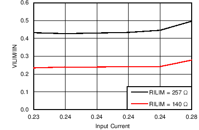
- Added spec for IIN/IILIM ratio Go
Changes from E Revision (December 2013) to F Revision
- Added 处理额定值表,特性 说明 部分、器件功能模式、应用和实施 部分、电源相关建议 部分、布局 部分、器件和文档支持 部分以及机械、封装和可订购信息 部分Go
- Deleted the minimum spec for RILIM-SHORT and changed the typical value to 55 ohm and maximum spec to 75 ohm.Go
- Changed VLDO values to (4.65, 4.85, 5.04) and added description in the second column.Go
Changes from D Revision (July 2013) to E Revision
- Changed VDPM pin desctiption from "......sets a default of 4.36V" to ".......sets a default of 4.68V" Go
- Changed text string in the VIN_DLM settings description from: "The ISET resistor must be floated in order to avoid an internal fault." to: "The ISET resistor must be connected in order to avoid an unstable charging state."Go
- Changed text string in the Sleep Mode description from: "...sends a single 256μs pulse is sent on the STAT and INT outputs..." to: "...sends a single 256µs pulse on the STAT and INT outputs..."Go
- Changed text string in the Input Over-Voltage Protection description from: "...turns the battery FET, sends a single 256-μs pulse is sent on the STAT and INT outputs..." to "...turns on the battery FET, sends a single 256-μs pulse on the STAT and INT outputs....."Go
- Added Serial Interface DescriptionGo
- Changed Register #3 description, B1(4)(5) Name from: "USB_DET_1/EN1" to: "USB_DET_1/EN2"Go
- Changed Register #3 description, B0(LSB) Name from: "USB_DET_0/EN0" to: "USB_DET_0/EN1"Go
- Changed Register #3 description, B1(4)(5) and B0(LSB) FUNCTION entries from: "Return USB detection result or pin EN1/EN0 status –" to "Return USB detection result or pin EN2/EN1 status –" ; changed 00 - DCP detected / from: "EN1=0, EN0=0" to: "EN2=0, EN1=0"; changed 01 - CDP detected / from: "EN1=0, EN0=1" to: "EN2=0, EN1=1"; changed 10 - SDP detected / from: "EN1=1, EN0=0" to: "EN2=1, EN1=0"; and changed 11 - Apple/TT or non-standard adaptor detected / from: "EN1=1, EN0=1" to: "EN2=1, EN1=1", respectively.Go
Changes from C Revision (June 2013) to D Revision
- Changed VDPM Pin Description regulator reference from "1.23V" to "1.2" Go
- Changed text string in D+/D- pin description from "....will remain low..." to "...will remain high impedance..."Go
- Added SCL and SDA to Pin Voltage Range spec in the Absolute Maximum Ratings tableGo
- Changed spec conditions for Output Current (Continuous), from "IN, SW, SYS, BAT" to "IN, SYS, BAT " in ABS Max Ratings table Go
- Changed Figure 20 Go
- Added text to NTC Monitor description for clarification.Go
- Added text to Safety Timer description for clarification.Go
- Changed Fault Condition from "Input Good" to "Input Fault & LDO Low" in Fault Conditions table.Go
- Changed Register #2 Reset state from "1010 1100" to "xxxx 1100"Go
- Changed Register #4 Reset state from "0000 0000" to "1111 1000"Go
- Changed Bit B7, B6, B5, B4, B3 FUNCTION description from "(default 0)" to "(default 1)"Go
- Changed Register #4 Footnote (1) text from "...current is 500ma...." to " .....current is external.."Go
- Changed TS_EN description from "When set to a ‘1' the TS function is disabled ....." to "When set to a ‘0’, the TS function is disabled..."Go
- Added text to TS_STAT description for clarification.Go
- Changed Register #7, Bit B3 FUNCTION description from "...if TERM is true or EN_PTM is true..." to "if TERM is true or Force PTM s true..."Go
Changes from B Revision (May 2013) to C Revision
- Deleted 从器件 bq24250YFF、bq24251YFF、bq24251RGE 和 bq24253RGE 中删除了“预览”状态注释Go
Changes from A Revision (March 2013) to B Revision
- Added 在“订购信息”表中向器件添加了“预览”状态(bq24250RGER 和 bq24250RGET 除外)Go
Changes from * Revision (October 2012) to A Revision
- 从“产品简介”更改成了“完整的产品说明书”Go
- Added Typical Characteristics graphsGo
- Changed Equation (3)Go
- Changed text in the F/S Mode Protocol section from "...to either transmit data to the slave (R/W bit 1) or receive data from the slave (R/W bit 0" to "...to either transmit data to the slave (R/W bit 0) or receive data from the slave (R/W bit 1)" for clarification.Go
5 说明 (续)
电源路径管理功能使得 bq24251 和 bq24253 能够在对电池进行独立充电的同时通过一个高效的直流/直流转换器为系统供电。此充电器一直监视电池电流并在系统负载所需电流高于输入电流限值时减小充电电流。该减小的充电电流可实现正常的充电终止并且使得系统能够在电池组有缺陷或不存在电池组的情况下运行。此外,该减小的充电电流使得即使在电池已完全放电或没有电池的情况下也能够瞬时启动系统。当适配器无法提供峰值系统电流时,此电源路径管理架构还允许电池补充系统电流要求。该电流要求补充支持使用较小的适配器。
电池充电分为四个阶段:涓流充电、预充电、恒定电流和恒定电压。在所有充电阶段,一个内部控制环路监视 IC 结温并且在超过内部温度阈值时减小充电电流。此外,还包括一个基于电压且符合 JEITA 标准的电池组热敏电阻器监控输入 (TS),用于监控电池温度,以实现安全充电。
6 Device Options
| DEVICE | DEFAULT OVP | D+/D- OR EN1/EN2 | INT OR PG | DEFAULT VOREG | MINSYS | TS PROFILE | I2C OR STAND ALONE | I2C ADDRESS |
|---|---|---|---|---|---|---|---|---|
| bq24251 | 10.5 V | D+/D- | PG | 4.2 V | 3.5V | JEITA | I2C + SA | 0x6A |
| bq24253 | 10.5 V | D+/D- and EN1/EN2 |
PG | 4.2 V | 3.5 V | JEITA | SA Only | N/A |
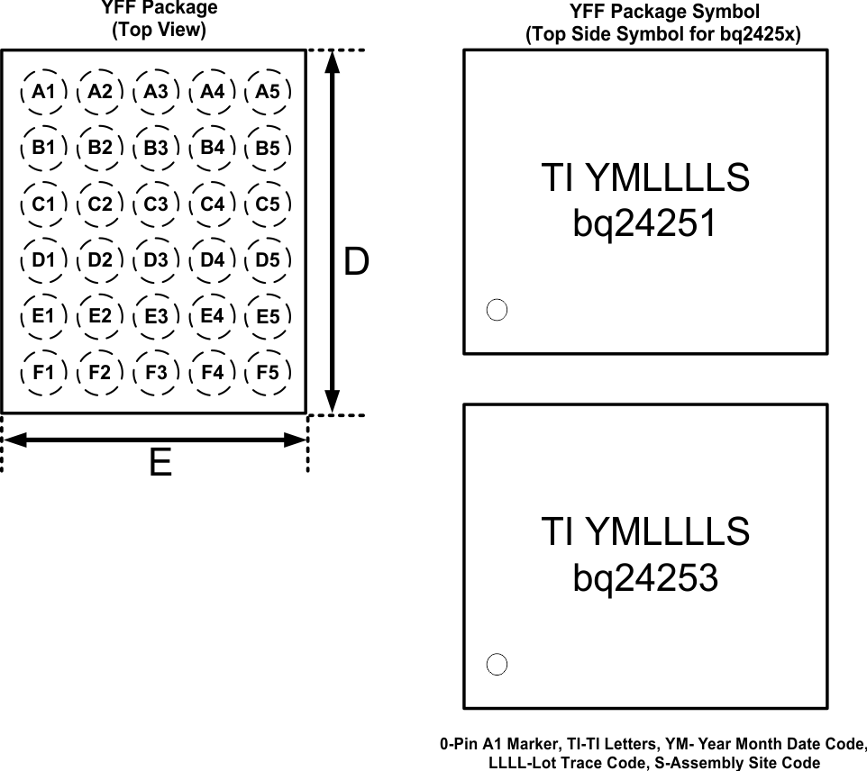
7 Pin Configuration and Functions
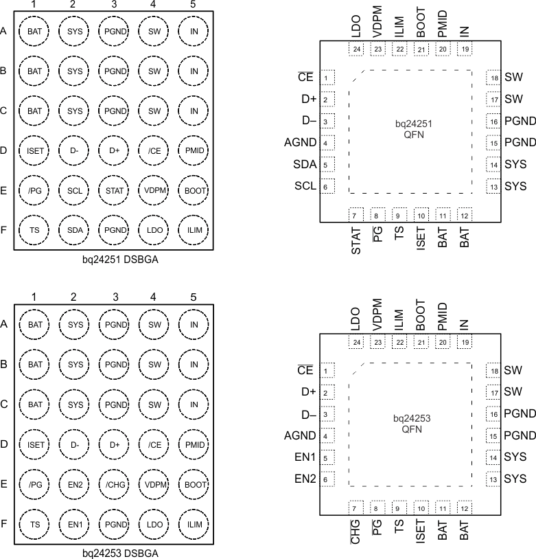
Pin Functions
| PIN | I/O | DESCRIPTION | ||||
|---|---|---|---|---|---|---|
| NAME | bq24251 | bq24253 | ||||
| YFF | RGE | YFF | RGE | |||
| IN | A5,B5,C5 | 19 | A5,B5,C5 | 19 | I | Input power supply. IN is connected to the external DC supply (AC adapter or USB port). Bypass IN to PGND with >2μF ceramic capacitor |
| PMID | D5 | 20 | D5 | 20 | I | Connection between blocking FET and high-side FET. |
| SW | A4, B4, C4 | 17–18 | A4, B4, C4 | 17–18 | O | Inductor Connection. Connect to the switching side of the external inductor. |
| BOOT | E5 | 21 | E5 | 21 | I | High Side MOSFET Gate Driver Supply. Connect a 0.033μF ceramic capacitor (voltage rating > 15V) from BOOT to SW to supply the gate drive for the high side MOSFETs. |
| PGND | A3, B3, C3, F3 | 15–16 | A3, B3, C3, F3 | 15–16 | Ground terminal. Connect to the ground plane of the circuit. | |
| SYS | A2, B2, C2 | 13–14 | A2, B2, C2 | 13–14 | I | System Voltage Sense and switched-mode power supply (SMPS) output filter connection. Connect SYS to the system output at the output bulk capacitors. Bypass SYS locally with >20μF. |
| BAT | A1, B1, C1 | 11–12 | A1, B1, C1 | 11–12 | I/O | Battery Connection. Connect to the positive terminal of the battery. Additionally, bypass BAT with a >1μF capacitor. |
| TS | F1 | 9 | F1 | 9 | I | Battery Pack NTC Monitor. Connect TS to the center tap of a resistor divider from LDO to GND. The NTC is connected from TS to GND. The TS function provides 4 thresholds for JEITA or PSE compatibility. See the NTC Monitor section for more details on operation and selecting the resistor values. |
| VDPM | E4 | 23 | E4 | 23 | I | Input DPM Programming Input. Connect a resistor divider between IN and GND with VDPM connected to the center tap to program the Input Voltage based Dynamic Power Management threshold (VIN_DPM). The input current is reduced to maintain the supply voltage at VIN_DPM. The reference for the regulator is 1.2V. Short pin to GND if external resistors are not desired—this sets a default of 4.68V for the input DPM threshold. |
| ISET | D1 | 10 | D1 | 10 | I | Charge Current Programming Input. Connect a resistor from ISET to GND to program the fast charge current. The charge current is programmable from 300mA to 2A. |
| ILIM | F5 | 22 | F5 | 22 | I | Input Current Limit Programming Input. Connect a resistor from ILIM to GND to program the input current limit for IN. The current limit is programmable from 0.5A to 2A. ILIM has no effect on the USB input. If an external resistor is not desired, short to GND for a 2A default setting. |
| CE | D4 | 1 | D4 | 1 | I | Charge Enable Active-Low Input. Connect CE to a high logic level to place the battery charger in standby mode. |
| EN1 | – | – | F2 | 5 | I | Input Current Limit Configuration Inputs. Use EN1, and EN2 to control the maximum input current and enable USB compliance. See Table 1 for programming details. |
| EN2 | – | – | E2 | 6 | I | |
| CHG | – | – | E3 | 7 | O | Charge Status Open Drain Output. CHG is pulled low when a charge cycle starts and remains low while charging. CHG is high impedance when the charging terminates and when no supply exists. CHG does not indicate recharge cycles. |
| PG | E1 | 8 | E1 | 8 | O | Power Good Open Drain Output. PG is pulled low when a valid supply is connected to IN. A valid supply is between VBAT+VSLP and VOVP. If no supply is connected or the supply is out of this range, PG is high impedance. |
| STAT | E3 | 7 | – | – | O | Status Output. STAT is an open-drain output that signals charging status and fault interrupts. STAT pulls low during charging. STAT is high impedance when charging is complete or the charger is disabled. When a fault occurs, a 256μs pulse is sent out as an interrupt for the host. STAT is enabled/disabled using the EN_STAT bit in the control register. STAT will indicate recharge cycles. Connect STAT to a logic rail using an LED for visual indication or through a 10kΩ resistor to communicate with the host processor. |
| INT | – | – | – | – | O | Status Output. INT is an open-drain output that signals charging status and fault interrupts. INT pulls low during charging. INT is high impedance when charging is complete or the charger is disabled. When a fault occurs, a 256μs pulse is sent out as an interrupt for the host. INT will indicate recharge cycles. Connect INT to a logic rail through a 10kΩ resistor to communicate with the host processor. |
| SCL | E2 | 6 | – | – | I | I2C Interface Clock. Connect SCL to the logic rail through a 10kΩ resistor. |
| SDA | F2 | 5 | – | – | I/O | I2C Interface Data. Connect SDA to the logic rail through a 10kΩ resistor. |
| D+ | D3 | 2 | D3 | 2 | I | BC1.2 compatible D+/D– Based Adapter Detection. Detects DCP, SDP, and CDP. Also complies with the unconnected dead battery provision clause. D+ and D- are connected to the D+ and D– outputs of the USB port at power up. Also includes the detection of Apple™ and TomTom™ adapters where a 500mA input current limit is enabled. The PG pin will remain high impedance until the detection has completed. |
| D– | D2 | 3 | D2 | 3 | I | |
| LDO | F4 | 24 | F4 | 24 | O | LDO output. LDO is regulated to 4.9V and drives up to 50mA. Bypass LDO with a 1μF ceramic Capacitor. LDO is enabled when VUVLO < VIN <18V. |
| AGND | – | 4 | – | 4 | Analog Ground for QFN only. Connect to the thermal pad and the ground plane of the circuit. | |
8 Specifications
8.1 Absolute Maximum Ratings(1)
over operating free-air temperature range (unless otherwise noted)8.2 ESD Ratings
| VALUE | UNIT | ||||
|---|---|---|---|---|---|
| V(ESD) | Electrostatic discharge | Human body model (HBM), per ANSI/ESDA/JEDEC JS-001, all pins(1) | ±2000 | V | |
| Charged device model (CDM), per JEDEC specification JESD22-C101, all pins(2) | ±500 | ||||
8.3 Recommended Operating Conditions
All voltages are with respect to PGND if not specified. Currents are positive into, negative out of the specified terminal. Consult Packaging Section of the data book for thermal limitations and considerations of packages| MIN | MAX | UNIT | ||
|---|---|---|---|---|
| VIN | IN voltage range | 4.35 | 18(1) | V |
| IN operating voltage range | 4.35 | 10.5 | ||
| IIN | Input current | 2 | A | |
| ICHG | Current in charge mode, BAT | 2 | A | |
| IDISCHG | Current in discharge mode, BAT | 4 | A | |
| RISET | Charge current programming resistor range | 75 | Ω | |
| RILIM | Input current limit programming resistor range | 105 | Ω | |
| PIN | Input Power | 12 | W | |
| TJ | Operating junction temperature range | 0 | 125 | °C |
8.4 Thermal Information
| THERMAL METRIC(1) | YFF (30 PINS) |
RGE (24 PINS) |
UNIT | |
|---|---|---|---|---|
| RθJA | Junction-to-ambient thermal resistance | 76.5 | 32.9 | °C/W |
| RθJCtop | Junction-to-case (top) thermal resistance | 0.2 | 32.8 | °C/W |
| RθJB | Junction-to-board thermal resistance | 44 | 10.6 | °C/W |
| ψJT | Junction-to-top characterization parameter | 1.6 | 0.3 | °C/W |
| ψJB | Junction-to-board characterization parameter | 43.4 | 10.7 | °C/W |
| RθJCbot | Junction-to-case (bottom) thermal resistance | N/A | 2.3 | °C/W |
8.5 Electrical Characteristics
VUVLO < VIN < VOVP and VIN > VBAT+VSLP, TJ = 0ºC-125°C and TJ = 25°C for typical values (unless otherwise noted)8.6 Typical Characteristics
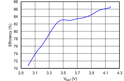
| VBAT = 3.8 V | VIN = 5 V | VREG = 4.2 V |
| ICHG = 0.5 A | ILIM = 1 A |
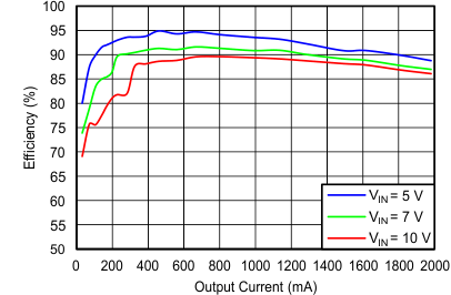
| ICHG = 2 A | VIN = 5 V | VREG = 4.2 V |
| VREG = 4.2 V | ||
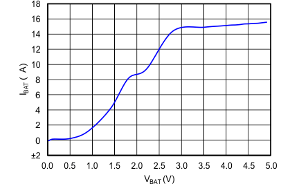
| VIN = 0 V | SYSOFF = 0 | Charge Enabled |
| BAT & SYS are Shorted | ||
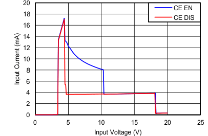
| Charge EN and DIS | No Battery and System | |
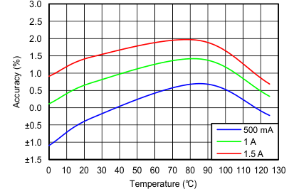
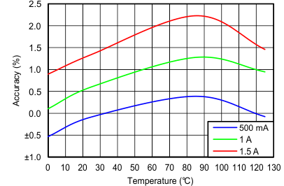 Figure 11. ICHG Accuracy with Internal Settings, VBAT = 3.3 V
| VBAT = 3.8 V | VIN = 6 V | VREG = 4.2 V |
| ICHG = 1 A | ILIM = 1 A |
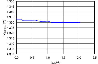
| VIN = 5 V | No Battery | ILIM = 2 A |
| VREG = 4.2 V | Charge Disable |
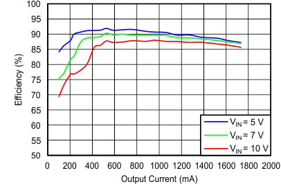
| VREG = 3.6 V | ||
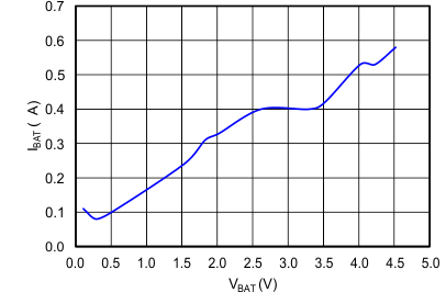
| VIN = 0 V | SYSOFF = 1 | Charge Enabled |
| BAT & SYS are Shorted | ||
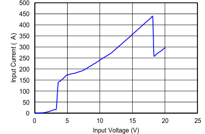
| Charge EN | Hi-Z EN |
| VBAT = 3.8 V | VIN = 5 V | VREG = 4.2 V |
| ILIM = 2 A |
| VBAT = 3.9 V | VOVP = 10.5 V | |
| ICHG = 1 A | ILIM = 1 A |
9 Detailed Description
9.1 Overview
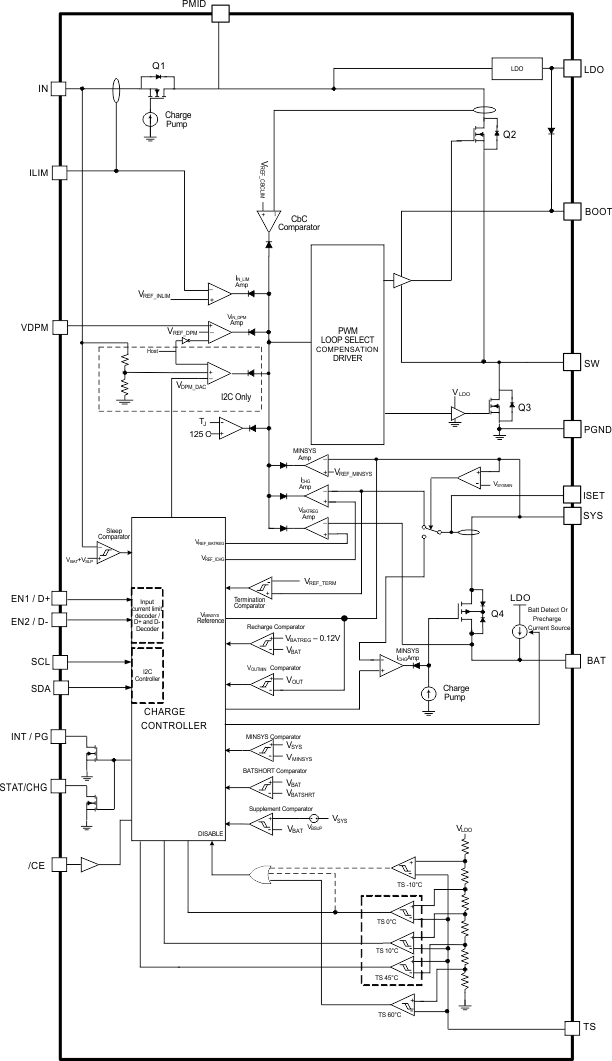
The bq2425x is a highly-integrated, single-cell, Li-Ion battery charger with integrated current sense resistors targeted for space-limited, portable applications with high-capacity batteries. The single-cell charger has a single input that operates from either a USB port or AC wall adapter for a versatile solution.
9.2 Functional Block Diagram
9.3 Feature Description
9.3.1 Charge Profile
The bq2425x family provides a switch-mode buck regulator with output power path and a charge controller to provide optimum performance over the full battery charge cycle. The control loop for the buck regulator has 7 primary feedback loops that can set the duty cycle:
- Constant Current (CC)
- Constant Voltage (CV)
- Minimum System Voltage (MINSYS)
- Input Current (IILIM)
- Input Voltage (VIN_DPM)
- Die Temperature
- Cycle by Cycle Current
The feedback with the minimum duty cycle will be chosen as the active loop. The bq24251 and bq24253 support a precision Li-Ion or Li-Polymer charging system for single-cell applications. The Dynamic Power Path Management (DPPM) feature regulates the system voltage to a minimum of VMINSYS, so that startup is enabled even with a missing or deeply discharged battery. This provides a much better overall user experience in mobile applications. Figure 15 illustrates a typical charge profile while also demonstrating the minimum system output voltage regulation.
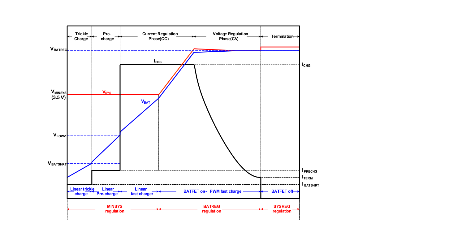 Figure 15. bq24250 Charge Profile and Minimum System Output Voltage Regulation
Figure 16 demonstrates a measured charge profile with the bq2425X while charging a 2700mAh Li-Ion battery at a charge rate of 1A.
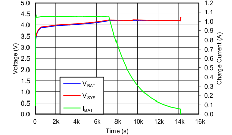
| ICHG = 1 A |
Figure 17 illustrates the precharge behavior of the above charge profile by narrowing the time axis to 0 – 120 seconds.
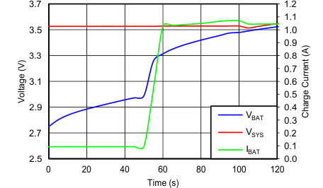
| ICHG = 1 A |
9.3.2 EN1 and EN2 Pins
The bq24251 is an I2C and stand-alone part. The EN1 and EN2 are not available for this spin but the D+/D- are available to support the BC1.2 D+/D- Based Adapter Detection. It detects DCP, SDP, and CDP. Also it complies with the unconnected dead battery provision clause. D+ and D- pins are connected to the D+ and D- outputs of the USB port at power up. Also includes the detection of AppleTM and TomTomTM adapters where a 500 mA input current limit is enabled. The PG pin will remain high impedance state until the detection is completed.
The bq24253 is a stand-alone part only. Both of the D+/D- and EN1/EN2 are available for this spin. During power up, the device checks first for the D+/D-. The EN1 and EN2 do not take effect until D+/D- detection routine is over and a change on the status of the EN1 and EN2 occurred.
When the input current limit pins change state, the VIN_DPM threshold changes as well. See Table 1 for the detailed truth table:
Table 1. EN1 and EN2 Truth Table(1)
| EN2 | EN1 | Input Current Limit | VIN_DPM Threshold |
|---|---|---|---|
| 0 | 0 | 500mA | 4.36V |
| 0 | 1 | Externally programmed by ILIM (up to 2.0A) | Externally programmed VDPM |
| 1 | 0 | 100mA | 4.36V |
| 1 | 1 | Input Hi-Z | None |
9.3.3 External Settings: ISET, ILIM and VIN_DPM
If the external resistor settings are used, the following equations can be followed to configure the charge settings.
The fast charge current resistor (RISET) can be set by using the following formula:

Where IFC is the desired fast charge current setting in Amperes.
The input current limit resistor (RILIM) can be set by using the following formula:

Where IIC is the desired input current limit in Amperes.
Based on the application diagram reference designators, the resistor R1 and R2 can be calculated as follows to set VIN_DPM:
VIN_DPM should be chosen first along with R1. Choosing R1 first will ensure that R2 will be greater than the resistance chosen. This is the case since VIN_DPM should be chosen to be greater than 2x VREF_DPM.
If external resistors are not desired in order to reduce the BOM count, the VDPM and the ILIM pins can be shorted to set the internal defaults. The ISET resistor must be connected in order to avoid an unstable charging state. Note that floating the ILIM pin will result in zero charge current if the external ISET is configured via the I2C register. Table 2 summarizes the settings when the ILIM, ISET, and VIN_DPM pins are shorted to GND:
Table 2. ILIM, VDPM, and ISET Short Behaviors
| PIN SHORTED | BEHAVIOR |
|---|---|
| ILIM | Input current limit = 2A |
| VDPM | VIN_DPM = 4.68V |
| ISET | Fault—Charging Suspended |
9.3.4 BC1.2 D+/D– Detection
The bq24251 and the bq24253 include a fully BC1.2 compatible D+/D– source detection. This detection supports the following types of ports:
- DCP (dedicated charge port)
- CDP (charging downstream port)
- SDP (standard downstream port)
- Apple™/TomTom™ ports
This D+/D– detection algorithm does not support ACA (accessory charge adapter) identification, but the input current will default to 500 mA when a charge port is attached to the ACA and bq24251/3 is connected to the OTG port.
The D+/D– detection algorithm is only active when the device is in standalone mode (e.g. the host is not communicating with the device and the watch dog timer has expired). However, when the device is in host mode (e.g. host is communicating via I2C to the device) writing a ‘1’ to register 0x04 bit location 4 (DPDM_EN) forces the device to perform a D+/D– detection. This allows the D+/D– detection to be enabled in both host mode and default mode. The current limit will not be implemented in host mode.
As described previously, the bq24253 is a stand-alone part only. Both of the D+/D- and EN1/EN2 are available for this spin. The below flow diagram illustrates the behavior of the bq24253 in D+/D- detection and the effect of the EN1/EN2. During power up, the device checks first for the D+/D-. The EN1 and EN2 do not take effect until D+/D- detection routine is over and a change on the status of the EN1 and EN2 occurred.
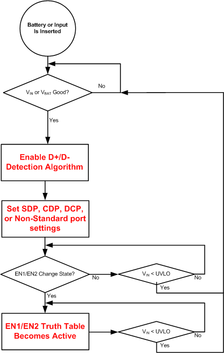 Figure 18. bq24253 D+/D- and EN1/EN2
The D+/D– detection algorithm has 5 primary states. These states are termed the following:
- Data Contact Detect
- Primary Detection
- Secondary Detection
- Non-standard Adapter Detection (for Apple™ / TomTom™)
- Detection Configuration
The DCD state determines if the device has properly connected to the D+/D– lines. If the device is not in host mode and VBUS is inserted (or DPDM_EN is true) the device enters the DCD state and enable the appropriate algorithm. If the DCD timer expires, the device enters the Non-standard Adapter Detection (for Apple™ / TomTom™) state. Otherwise it enters the Primary Detection state.
When entering the Primary Detection state, the appropriate algorithm is enabled to determine whether to enter the secondary detection state for DCP and CDP or the secondary detection state for SDP/Non-Standard adaptors.
The non-standard adapter detection state for Apple™ / TomTom™ tests for the unique conditions for these non-standard adapters. If the algorithm passes the unique conditions found with these adapters, it proceeds to the Detection Configuration state. Otherwise it reverts back to the primary detection state.
The secondary detection state determines whether the input port is a DCP, CDP, SDP, or other non-standard adapters. If the Primary Detection state indicated that the input port is either a DCP or CDP, the device enables the appropriate algorithm to differentiate between the two. If the Primary Detection state indicated that the input port is either a SDP or non-standard adapter, the device enables the appropriate algorithm to differentiate between these two ports. Once complete, the device continues to the Detection Configuration state.
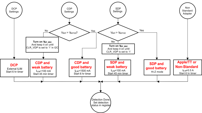 Figure 19. Detection Configuration State
The detection configuration state sets the input current limit of the device along with the charge timer. The exception to the CDP and the SDP settings are due to the Dead Battery Provision (DBP) clause for unconnected devices. This clause states that the device can pull a maximum of 100mA when not connected due to a dead battery. During the battery wakeup time, the device sources a voltage on the D+ pin in order to comply with the DBP clause. Once the battery is good, the system can clear the D+ pin voltage by writing a ‘1’ to address 0x07 bit position 4 (CLR_VDP). The device must connect to the host within 1sec of clearing the D+ pin voltage per the DPB clause.
A summary of the input current limits and timer configurations for each charge port type are found in Table 3.
Table 3. D+/D– Detection Results per Charge Port Type
| CHARGE PORT TYPE | INPUT CURRENT LIMIT | CHARGE TIMER |
|---|---|---|
| DCP | External ILIM | 6 hours |
| CDP Dead Battery | 100 mA | 45 minutes |
| CDP Good Battery | 1500 mA | 6 hours |
| SDP Dead Battery | 100 mA | 45 minutes |
| SDP Good Battery | Hi-Z | N/A |
| Non-Standard | 500 mA | 6 hours |
9.3.5 Transient Response
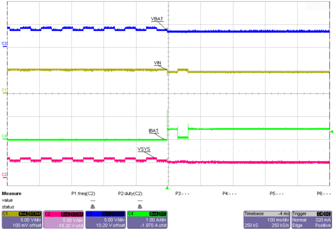
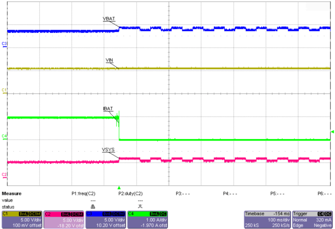
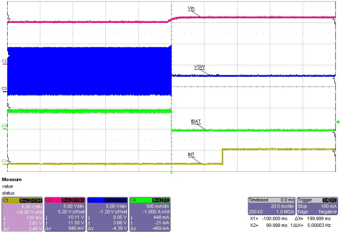
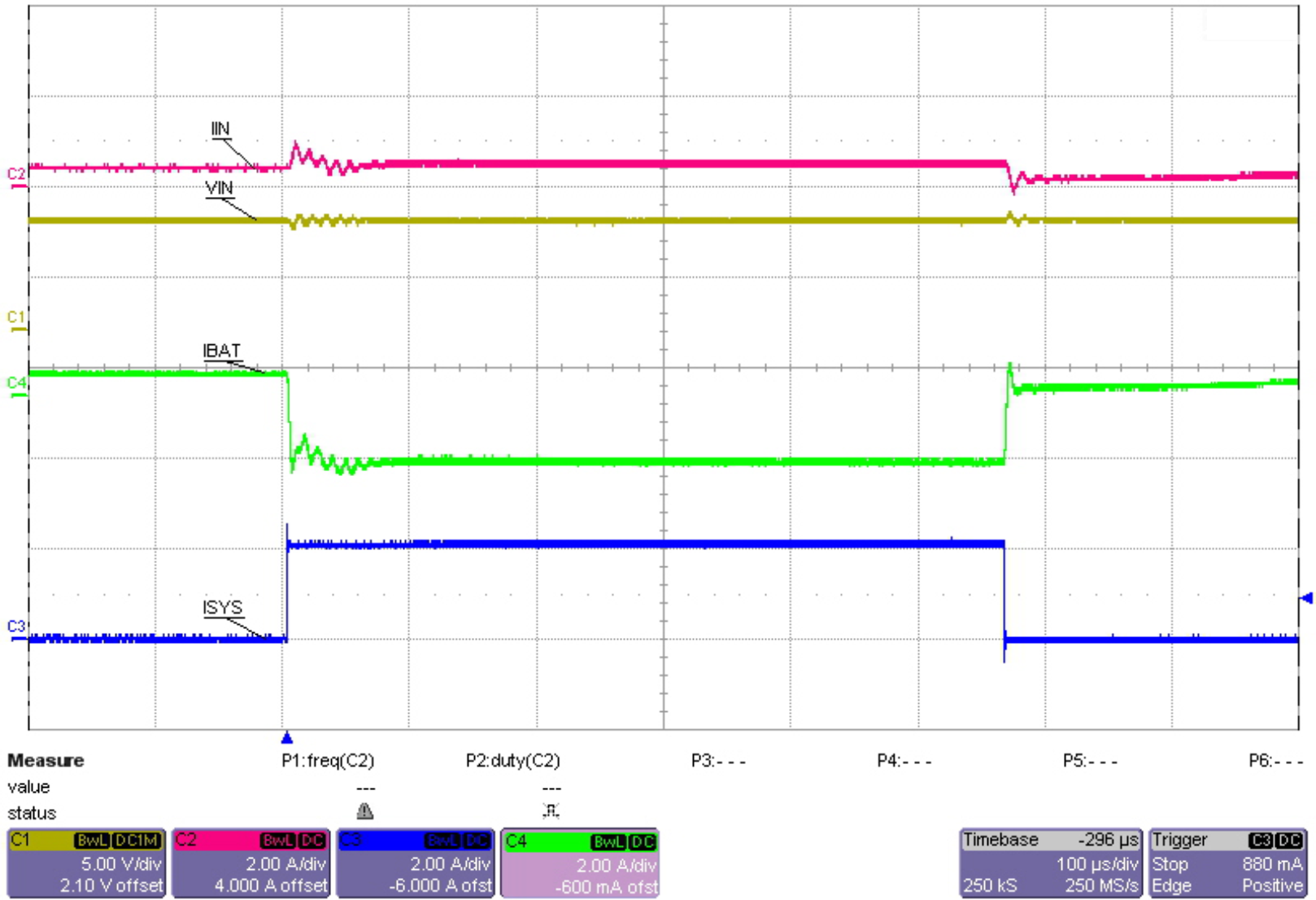
The bq24251 and bq24253 include an advanced hybrid switch mode control architecture. When the device is regulating the charge current (fast-charge), a traditional voltage mode control loop is used with a Type-3 compensation network. However, the bq24251 and bq24253 switch to a current-mode control loop when the device enters voltage regulation. Voltage regulation occurs in three charging conditions: 1) Minimum system voltage regulation (battery below MINSYS), 2) Battery voltage regulation (IBAT < ICHG), and 3) Charge Done (VSYS = VBAT + 3.5%). This architecture allows for superior transient performance when regulating the voltage due to the simplification of the compensation when using current mode control. The below transient response plot illustrates a 0A to 2A load step with 4.7 ms full cycle and 12% duty cycle. A 3.9 V Li-Ion battery is used. The input voltage is set to 5 V, charge current is set to 0.5 A and the input current is limited to 0.5 A. Note that a high line impedance input supply was used to indicate a realistic input scenario (adapter and cable). This is illustrated by the change in VIN seen at the input of the IC.
Figure 33 shows a ringing at both the input voltage and the input current. This is caused by the input current limit speed up comparator.
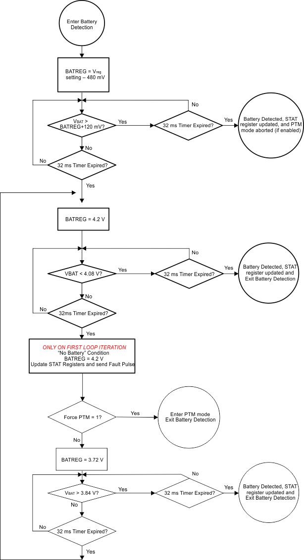
9.3.6 AnyBoot Battery Detection
The bq2425x family includes a sophisticated battery detection algorithm used to provide the system with the proper status of the battery connection. The AnyBoot battery algorithm also guarantees the detection of voltage based battery protectors that may have a long closure time (due to the hysteresis of the protection switch and the cell capacity). The AnyBoot battery detection algorithm utilizes a dual-voltage based detection methodology where the system rail switches between two primary voltage levels. The period of the voltage level shift is 64ms and therefore the power supply rejection of the down-system electronics detects this shift as essentially DC.
The AnyBoot algorithm has essentially 3 states. The 1st state is used to determine if the device has terminated with a battery attached. If it has terminated due to the battery not being present, then the algorithm moves to the 2nd and 3rd states. The 2nd and 3rd states shift the system voltage level between 4.2 V and 3.72 V. In each state there are comparator checks to determine if a battery has been inserted. The two states guarantees the detection of a battery even if the voltage of the cell is at the same level of the comparator thresholds. The algorithm will remain in states 2 and 3 until a battery has been inserted. The flow diagram details for the Anyboot algorithm are shown in Figure 20.
9.3.7 Input Voltage Based DPM
During normal charging process, if the input power source is not able to support the programmed or default charging current, the supply voltage deceases. Once the supply drops to VIN_DPM, the input current limit is reduced down to prevent the further drop of the supply. When the IC enters this mode, the charge current is lower than the set. This feature ensures IC compatibility with adapters with different current capabilities without a hardware change.
9.3.8 Sleep Mode
The bq2425x enters the low-power sleep mode if the voltage on VIN falls below sleep-mode entry threshold, VBAT+VSLP, and VIN is higher than the under-voltage lockout threshold, VUVLO. This feature prevents draining the battery during the absence of VIN. When VIN < VBAT+VSLP, the bq2425x turns off the PWM converter, turns on the battery FET, sends a single 256-µs pulse on the STAT and INT outputs and the FAULT/STAT bits of the status registers are updated in the I2C. Once VIN > VBAT+VSLP with the hysteresis, the FAULT bits are cleared and the device initiates a new charge cycle.
9.3.9 Input Over-Voltage Protection
The bq2425x provides over-voltage protection on the input that protects downstream circuitry. The built-in input over-voltage protection to protect the device and other components against damage from overvoltage on the input supply (Voltage from VIN to PGND). When VIN > VOVP, the bq2425x turns off the PWM converter, turns on the battery FET, sends a single 256-μs pulse on the STAT and INT outputs and the FAULT/STAT bits of the status registers and the battery/supply status registers are updated in the I2C. Once the OVP fault is removed, the FAULT bits are cleared and the device returns to normal operation.
9.3.10 NTC Monitor
The bq24251 and bq24253 include the integration of an NTC monitor pin that complies with the JEITA specification (PSE also available upon request). The voltage based NTC monitor allows for the use of any NTC resistor with the use of the circuit shown in Figure 21.
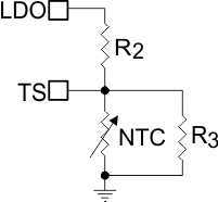 Figure 21. Voltage Based NTC Circuit
The use of R3 is only necessary when the NTC does not have a beta near 3500K. When deviating from this beta, error will be introduced in the actual temperature trip thresholds. The trip thresholds are summarized below which are typical values provided in the specification table.
Table 4. Ratiometric TS Trip Thresholds for JEITA Compliant Charging
| TS THRESHOLDS | VTS/VLDO |
|---|---|
| VHOT | 30.0% |
| VWARM | 38.3% |
| VCOOL | 56.5% |
| VCOLD | 60% |
When sizing for R2 and R3, it is best to solve two simultaneous equations that ensure the temperature profile of the NTC network will cross the VHOT and VCOLD thresholds. The accuracy of the VWARM and VCOOL thresholds will depend on the beta of the chosen NTC resistor. The two simultaneous equations are shown below:
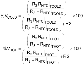
Where the NTC resistance at the VHOT and VCOLD temperatures must be resolved as follows:

To be JEITA compliant, TCOLD must be 0°C and THOT must be 60°C. If an NTC resistor is chosen such that the beta is 4000K and the nominal resistance is 10 kΩ, the following R2 and R3 values result from the above equations:
R2 = 5 kΩ
R3 = 9.82 kΩ
Figure 22 illustrates the temperature profile of the NTC network with R2 and R3 set to the above values.
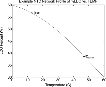 Figure 22. Voltage Based NTC Circuit Temperature Profile
For JEITA compliance, the TCOOL and TWARM levels are to be 10°C and 45°C respectively. However, there is some error due to the variation in beta from 3500K. As shown above, the actual temperature points at which the NTC network crosses the VCOOL and VWARM are 13°C and 47°C respectively. This error is small but should be considered when choosing the final NTC resistor.
Once the resistors are configured, the internal JEITA algorithm applies the profile shown in Figure 23at each trip point for battery voltage regulation and charge current regulation. In order to ensure continuation of the charge process when an almost-full battery stops charging due to a cold temperature fault, it is recommended that a CE toggle is done on the I2C or CE pin.
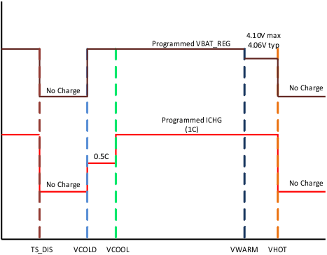 Figure 23. JEITA Profile for Voltage and Current Regulation Loops
9.3.11 Production Test Mode
To aid in end mobile device product manufacturing, the bq2425x includes a Production Test Mode (PTM), where the device is essentially a DC-DC buck converter. In this mode the input current limit to the charger is disabled and the output current limit is limited only by the inductor cycle-by-cycle current (e.g. 3.5A). The PTM mode can be used to test systems with high transient loads such as GSM transmission without the need of a battery being present.
As a means of safety, the Anyboot algorithm will determine if a battery is not present at the output prior to enabling the PTM mode. If a battery is present and the software attempts to enter PTM mode, the device will not enable PTM mode.
9.3.12 Safety Timer
At the beginning of charging process, the bq2425x starts the safety timer. This timer is active during the entire charging process. If charging has not terminated before the safety timer expires, the IC enters suspend mode where charging is disabled. The safety timer time is selectable using the I2C interface. A single 256μs pulse is sent on the STAT and INT outputs and the FAULT/ bits of the status registers are updated in the I2C. This function prevents continuous charging of a defective battery if the host fails to reset the safety timer. When 2xTMR_EN bit is set to “1”, the safety timer runs at a rate 2x slower than normal (the timer is extended) under the following conditions:
- Pre-charge or linear mode (minimum system voltage mode),
- During thermal regulation where the charge current is reduced,
- During TS fault where the charge current is reduced due to temperature rise on the battery, input current limit
The safety timer is suspended during OVP, TS fault where charge is disabled, thermal shut down, and sleep mode. Removing the battery causes the safety timer to be reset and NOT halted/paused.
9.3.13 Watchdog Timer
In addition to the safety timer, the bq24251 contains a 50-second watchdog timer that monitors the host through the I2C interface. Once a write is performed on the I2C interface, a watchdog timer is reset and started. The watchdog timer can be disabled by writing “0” on WD_EN bit of register #1. Writing “1” on that bit enables and resets the timer.
If the watchdog timer expires, the IC enters DEFAULT mode where the default charge parameters are loaded and charging continues. The I2C may be accessed again to re-initialize the desired values and restart the watchdog timer as long as the safety timer has not expired. Once the safety timer expires, charging is disabled.
9.3.14 Fault Modes
The bq2425x family includes several hardware fault detections. This allows for specific conditions that could cause a safety concern to be detected. With this feature, the host can be alleviated from monitoring unsafe charging conditions and also allows for a “fail-safe” if the host is not present. The table below summarizes the faults that are detected and the resulting behavior.
9.3.15 Dynamic Power Path Management
The bq24251 and bq24253 feature a SYS output that powers the external system load connected to the battery. This output is active whenever a valid source is connected to IN or BAT. The following discusses the behavior of SYS with a source connected to the supply or a battery source only.
When a valid input source is connected to the input and the charge is enabled, the charge cycle is initiated. In case of VBAT > ~3.5V, the SYS output is connected to VBAT. If the SYS voltage falls to VMINSYS, it is regulated to the VSYSREG threshold to maintain the system output even with a deeply discharged or absent battery. In this mode, the SYS output voltage is regulated by the buck converter and the battery FET is linearly regulated to regulate the charge current into the battery. The current from the supply is shared between charging the battery and powering the system load at SYS.
The dynamic power path management (DPPM) circuitry of the bq2425x monitors the current limits continuously and if the SYS voltage falls to the VMINSYS voltage, it adjusts charge current to maintain the minimum system voltage and supply the load on SYS. If the charge current is reduced to zero and the load increases further, the bq2425x enters battery supplement mode. During supplement mode, the battery FET is turned on and the battery supplements the system load.
If the battery is ever 5% above the regulation threshold, the battery OVP circuit shuts the PWM converter off and the battery FET is turned on to discharge the battery to safe operating levels. Battery OVP FAULT is shown in the I2C FAULT registers.
When no input source is available at the input and the battery is connected, the battery FET is turned on similar to supplement mode. The battery must be above VBATUVLO threshold to turn on the SYS output. In this mode, the current is not regulated; however, there is a short circuit current limit. If the short circuit limit is reached, the battery FET is turned off for the deglitch time. After the deglitch time, the battery FET is turned on to test and see if the short has been removed. If it has not, the FET turns off and the process repeats until the short is removed. This process is to protect the internal FET from over current.
9.4 Device Functional Modes
9.4.1 I2C Operation (Host Mode / Default Mode)
There are two primary modes of operation when interacting with the charge parameters of the bq24251 chargers: 1) Host mode operation where the I2C registers set the charge parameters, and 2) Default mode where the register defaults set the charge parameters.
Figure 24 illustrates the behavior of the bq24251 when transitioning between host mode and stand alone mode:
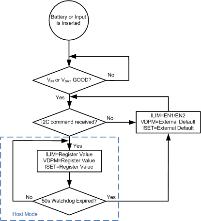 Figure 24. Host Mode and Stand Alone Mode Handoff
Once the battery or input is inserted and above the good thresholds, the device determines if an I2C command has been received in order to discern whether to operate from the I2C registers or the internal register defaults. In stand-alone mode the input current limit is set by the EN1/EN2 pins. If the watch dog timer is enabled, the device will enter stand alone operation once the watchdog timer expires and re-initiate the default charge settings.
9.5 Programming
9.5.1 Serial Interface Description
The bq2425x uses an I2C compatible interface to program charge parameters. I2C ™ is a 2-wire serial interface developed by NXP (formerly Philips Semiconductor, see I2C-Bus Specification, Version 5, October 2012). The bus consists of a data line (SDA) and a clock line (SCL) with pull-up structures. When the bus is idle, both SDA and SCL lines are pulled high. All the I2C compatible devices connect to the I2C bus through open drain I/O pins, SDA and SCL. A master device, usually a microcontroller or a digital signal processor, controls the bus. The master is responsible for generating the SCL signal and device addresses. The master also generates specific conditions that indicate the START and STOP of data transfer. A slave device receives and/or transmits data on the bus under control of the master device.
The bq2425x device works as a slave and supports the following data transfer modes, as defined in the I2C Bus™ Specification: standard mode (100 kbps) and fast mode (400 kbps). The interface adds flexibility to the battery charge solution, enabling most functions to be programmed to new values depending on the instantaneous application requirements. The I2C circuitry is powered from IN when a supply is connected.
The data transfer protocol for standard and fast modes is exactly the same; therefore, they are referred to as the F/S-mode in this document. The bq24251 device only supports 7-bit addressing. The device 7-bit address is defined as ‘1101010’ (0x6Ah).
To avoid I2C hang-ups, a timer (tI2CRESET) runs during I2C transactions. If the transaction takes longer than tI2CRESET, any additional commands are ignored and the I2C engine is reset. The timeout is reset with START and repeated START conditions and stops when a valid STOP condition is sent.
9.5.1.1 F/S Mode Protocol
The master initiates data transfer by generating a start condition. The start condition is when a high-to-low transition occurs on the SDA line while SCL is high, as shown in Figure 25. All I2C -compatible devices should recognize a start condition.
 Figure 25. START and STOP Condition
The master then generates the SCL pulses, and transmits the 7-bit address and the read/write direction bit R/W on the SDA line. During all transmissions, the master ensures that data is valid. A valid data condition requires the SDA line to be stable during the entire high period of the clock pulse (see Figure 26). All devices recognize the address sent by the master and compare it to their internal fixed addresses. Only the slave device with a matching address generates an acknowledge (see Figure 27) by pulling the SDA line low during the entire high period of the ninth SCL cycle. Upon detecting this acknowledge, the master knows that communication link with a slave has been established.
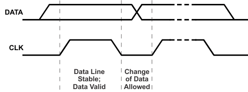 Figure 26. Bit Transfer on the Serial Interface
The master generates further SCL cycles to either transmit data to the slave (R/W bit 0) or receive data from the slave (R/W bit 1). In either case, the receiver needs to acknowledge the data sent by the transmitter. So an acknowledge signal can either be generated by the master or by the slave, depending on which one is the receiver. The 9-bit valid data sequences consisting of 8-bit data and 1-bit acknowledge can continue as long as necessary. To signal the end of the data transfer, the master generates a stop condition by pulling the SDA line from low to high while the SCL line is high (see Figure 25). This releases the bus and stops the communication link with the addressed slave. All I2C compatible devices must recognize the stop condition. Upon the receipt of a stop condition, all devices know that the bus is released, and wait for a start condition followed by a matching address. If a transaction is terminated prematurely, the master needs to send a STOP condition to prevent the slave I2C logic from remaining in a incorrect state. Attempting to read data from register addresses not listed in this section will result in 0xFFh being read out.
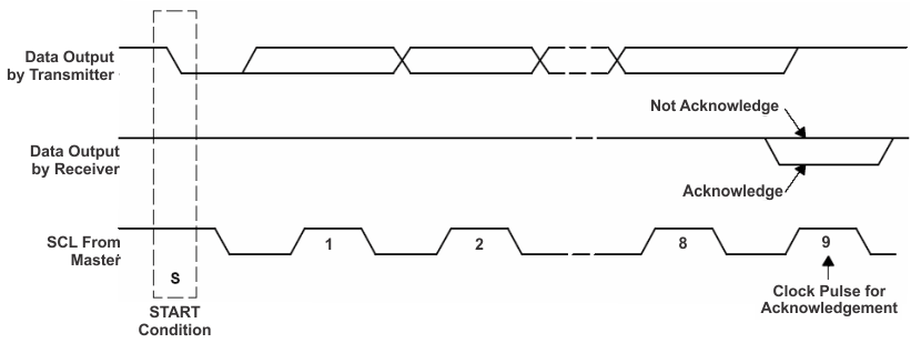 Figure 27. Acknowledge on the I2C Bus
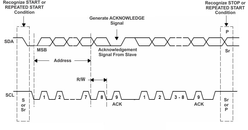 Figure 28. Bus Protocol
9.6 Register Maps
9.6.1 Register #1
Memory location: 00, Reset state: x0xx xxxx
| BIT | NAME | READ/WRITE | FUNCTION |
|---|---|---|---|
| B7(MSB) | WD_FAULT | Read only | Read:0 – No fault 1 – WD timeout if WD enabled |
| B6 | WD_EN | Read/Write | 0 – Disable 1 – Enable (also resets WD timer) |
| B5 | STAT_1 | Read only | 00 – Ready 01 – Charge in progress 10 – Charge done 11 – Fault |
| B4 | STAT_0 | Read only | |
| B3 | FAULT_3 | Read only | 0000 – Normal 0001 – Input OVP 0010 – Input UVLO 0011 – Sleep 0100 – Battery Temperature (TS) Fault 0101 – Battery OVP 0110 – Thermal Shutdown 0111 – Timer Fault 1000 – No Battery connected 1001 – ISET short 1010 – Input Fault and LDO low |
| B2 | FAULT_2 | Read only | |
| B1 | FAULT_1 | Read only | |
| B0(LSB) | FAULT_0 | Read only |
- WD_FAULT – ‘0’ indicates no watch dog fault has occurred, where a ‘1’ indicates a fault has previously occurred.
- WD_EN – Enables or disables the internal watch dog timer. A ‘1’ enables the watch dog timer and a ‘0’ disables it. '1' is default for bq24251 only.
- STAT – Indicates the charge controller status.
- FAULT – Indicates the faults that have occurred. If multiple faults occurred, they can be read by sequentially addressing this register (e.g. reading the register 2 or more times). Once all faults have been read and the device is in a non-fault state, the fault register will show “Normal”. Regarding the "Input Fault & LDO Low" the IC indicates this if LDO is low and at the same time the input is below UVLO or coming out of UVLO with LDO still low.
9.6.2 Register #2
Memory location: 01, Reset state: xxxx 1100
| BIT | NAME | READ/WRITE | FUNCTION |
|---|---|---|---|
| B7(MSB) | Reset | Write only | Write: 1 – Reset all registers to default values 0 – No effect |
| B6 | IIN_ILIMIT_2 | Read/Write | 000 – USB2.0 host with 100mA current limit 001 – USB3.0 host with 150mA current limit 010 – USB2.0 host with 500mA current limit 011 – USB3.0 host with 900mA current limit 100 – Charger with 1500mA current limit 101 – Charger with 2000mA current limit 110 – External ILIM current limit 111- No input current limit with internal clamp at 3A (PTM MODE) |
| B5 | IIN_ILIMIT_1 | Read/Write | |
| B4 | IIN_ILIMIT _0 | Read/Write | |
| B3 | EN_STAT | Read/Write | 0 – Disable STAT function 1 – Enable STAT function |
| B2 | EN_TERM | Read/Write | 0 – Disable charge termination 1 – Enable charge termination |
| B1 | CE | Read/Write | 0 – Charging is enabled 1 – Charging is disabled |
| B0 (LSB) | HZ_MODE | Read/Write | 0 – Not high impedance mode 1 – High impedance mode |
- IIN_LIMIT – Sets the input current limit level. When in host mode this register sets the regulation level. However, when in standalone mode (e.g. no I2C writes have occurred after power up or the WD timer has expired) the external resistor setting for IILIM sets the regulation level.
- EN_STAT – Enables and disables the STAT pin. When set to a ‘1’ the STAT pin is enabled and function normally. When set to a ‘0’ the STAT pin is disabled and the open drain FET is in HiZ mode.
- EN_TERM – Enables and disables the termination function in the charge controller. When set to a ‘1’ the termination function will be enabled. When set to a ‘0’ the termination function will be disabled. When termination is disabled, there are no indications of the charger terminating (i.e. STAT pin or STAT registers).
- CE – The charge enable bit which enables or disables the charge function. When set to a ‘0’, the charger operates normally. When set to a ‘1’, the charger is disables by turning off the BAT FET between SYS and BAT. The SYS pin continues to stay active via the switch mode controller if an input is present.
- HZ_MODE – Sets the charger IC into low power standby mode. When set to a ‘1’, the switch mode controller is disabled but the BAT FET remains ON to keep the system powered. When set to a ‘0’, the charger operates normally.
9.6.3 Register #3
Memory location: 02, Reset state: 1000 1111
| BIT | NAME | READ/WRITE | FUNCTION |
|---|---|---|---|
| B7(MSB) | VBATREG_5(1) | Read/Write | Battery Regulation Voltage: 640mV (default 1) |
| B6 | VBATREG_4(1) | Read/Write | Battery Regulation Voltage: 320mV (default 0) |
| B5 | VBATREG_3(1) | Read/Write | Battery Regulation Voltage: 160mV (default 0) |
| B4 | VBATREG_2(1) | Read/Write | Battery Regulation Voltage: 80mV (default 0) |
| B3 | VBATREG_1(1) | Read/Write | Battery Regulation Voltage: 40mV (default 1) |
| B2 | VBATREG_0(1) | Read/Write | Battery Regulation Voltage: 20mV (default 1) |
| B1(4)(5) | USB_DET_1/EN2 | Read Only | Return USB detection result or pin EN2/EN1 status – 00 – DCP detected / EN2=0, EN1=0 01 – CDP detected / EN2=0, EN1=1 10 – SDP detected / EN2=1, EN1=0 11 – Apple/TT or non-standard adaptor detected / EN2=1, EN1=1 |
| B0(LSB) | USB_DET_0/EN1 | Read Only |
- VBATREG – Sets the battery regulation voltage
- USB_DET/EN – Provides status of the D+/D– detection-results for spins that include the D+/D– pins or the state of EN1/EN2 for spins that include the EN1/EN2 pins
9.6.4 Register #4
Memory location: 03, Reset state: 1111 1000
| BIT | NAME | READ/WRITE | FUNCTION |
|---|---|---|---|
| B7(MSB) | ICHG_4(1) (2) | Read/Write | Charge current 800 mA – (default 1) |
| B6 | ICHG_3(1) (2) | Read/Write | Charge current: 400 mA – (default 1) |
| B5 | ICHG_2(1) (2) | Read/Write | Charge current: 200 mA – (default 1) |
| B4 | ICHG_1(1) (2) | Read/Write | Charge current: 100 mA – (default 1) |
| B3 | ICHG_0(1) (2) | Read/Write | Charge current: 50 mA – (default 1) |
| B2 | ITERM_2(3) | Read/Write | Termination current sense threshold: 100 mA (default 0) |
| B1 | ITERM_1(3) | Read/Write | Termination current sense threshold: 50 mA (default 0) |
| B0(LSB) | ITERM_0(3) | Read/Write | Termination current sense threshold: 25 mA (default 0) |
- ICHG – Sets the charge current regulation
- ITERM – Sets the current level at which the charger will terminate
9.6.5 Register #5
Memory location: 04, Reset state: xx00 x010
| BIT | NAME | READ/WRITE | FUNCTION |
|---|---|---|---|
| B7(MSB) | LOOP_STATUS1(1) | Read Only | 00 – No loop is active that slows down timer 01 – VIN_DPM regulation loop is active 10 – Input current limit loop is active 11 – Thermal regulation loop is active |
| B6 | LOOP_STATUS0(1) | Read Only | |
| B5 | LOW_CHG | Read/Write | 0 – Normal charge current set by 03h 1 – Low charge current setting 330mA (default 0) |
| B4 | DPDM_EN | Read/Write | 0 – Bit returns to 0 after D+/D– detection is performed 1 – Force D+/D– detection (default 0) |
| B3 | CE_STATUS | Read Only | 0 – CE low 1 – CE high |
| B2 | VINDPM_2 (2) | Read/Write | Input VIN-DPM voltage: 320mV (default 0) |
| B1 | VINDPM_1 (2) | Read/Write | Input VIN-DPM voltage: 160mV (default 1) |
| B0(LSB) | VINDPM_0 (2) | Read/Write | Input VIN-DPM voltage: 80mV (default 0) |
- LOOP_STATUS – Provides the status of the active regulation loop. The charge controller allows for only one loop can regulate at a time.
- LOW_CHG – When set to a ‘1’, the charge current is reduced 330mA independent of the charge current setting in register 0x03. When set to ‘0’, the charge current is set by register 0x03.
- DPDM_EN – Forces a D+/D- detection routine to be executed once a ‘1’ is written. This is independent of the input being supplied.
- CE_STATUS – Provides the status of the CE pin level. If the CE pin is forced high, this bit returns a ‘1’. If the CE pin is forced low, this bit returns a ‘0’.
- VINDPM – Sets the input VDPM level.
9.6.6 Register #6
Memory location: 05, Reset state: 101x 1xxx
| BIT | NAME | READ/WRITE | FUNCTION |
|---|---|---|---|
| B7(MSB) | 2XTMR_EN | Read/Write | 0 – Timer not slowed at any time 1 – Timer slowed by 2x when in thermal regulation, VIN_DPM or DPPM (default 1) |
| B6 | TMR_1 | Read/Write | Safety Timer Time Limit 00 – 0.75 hour fast charge 01 – 6 hour fast charge (default 01) 10 – 9 hour fast charge 11 – Disable safety timers |
| B5 | TMR_2 | Read/Write | |
| B4 | SYSOFF | Read/Write | 0 – SYSOFF disabled 1 – SYSOFF enabled |
| B3 | TS_EN | Read/Write | 0 – TS function disabled 1 – TS function enabled (default 1) |
| B2 | TS_STAT2 | Read only | TS Fault Mode: 000 – Normal, No TS fault 001 – TS temp > THOT (Charging suspended for JEITA and Standard TS) 010 – TWARM < TS temp < THOT (Regulation voltage is reduced for JEITA standard) 011 – TCOLD < TS temp < TCOOL (Charge current is reduced for JEITA standard) 100 – TS temp < TCOLD (Charging suspended for JEITA and Standard TS) 101 – TFREEZE < TS temp < TCOLD (Charging at 3.9V and 100mA and only for PSE option only) 110 – TS temp < TFREEZE (Charging suspended for PSE option only) 111 – TS open (TS disabled) |
| B1 | TS_STAT1 | Read only | |
| B0(LSB) | TS_STAT0 | Read only |
- 2xTMR_EN – When set to a ‘1’, the 2x Timer function is enabled and allows for the timer to be extended if a condition occurs where the charge current is reduced (i.e. VIN_DPM, thermal regulation, etc.). When set to a ‘0’, this function is disabled and the normal timer will always be executed independent of the current reduce conditions.
- SYSOFF – When set to a ‘1’ and the input is removed, the internal battery FET is turned off in order to reduce the leakage from the BAT pin to less than 1µA. Note that this disconnects the battery from the system. When set to a ‘0’, this function is disabled.
- TS_EN – Enables and disables the TS function. When set to a ‘0’ the TS function is disabled otherwise it is enabled. Only applies to spins that have a TS pin.
- TS_STAT – Provides status of the TS pin state for versions that have a TS pin. “100” indicates the TS temp < TCOLD and charging suspended for JEITA Standard. In order to ensure continuation of the charge process when an almost-full battery stops charging due to a cold temperature fault, it is recommended that a CE toggle is done on the I2C or CE pin.
9.6.7 Register #7
Memory location: 06, Reset state: 1110 0000
- VOVP – Sets the OVP level
- CLR_VDP – When the D+/D– detection has finished, some cases require the D+ pin to force a voltage of 0.6 V. This bit allows the system to clear the voltage prior to any communication on the D+/D– pins. A ‘1’ clears the voltage at the D+ pin if present.
- FORCE_BATDET – Forces battery detection and provides status of the battery presence. A logic ‘1’ enables this function.
- FORCE_PTM – Puts the device in production test mode (PTM) where the input current limit is disabled. Note that a battery must not be present prior to using this function. Otherwise the function will not be allowed to execute. A logic ‘1’ enables the PTM function.
10 Application and Implementation
NOTE
Information in the following applications sections is not part of the TI component specification, and TI does not warrant its accuracy or completeness. TI’s customers are responsible for determining suitability of components for their purposes. Customers should validate and test their design implementation to confirm system functionality.
10.1 Application Information
The bq2425x devices are high-efficiency switched-mode chargers. The device has integrated power FETs that are able to charge at up to a 2-A charging rate, and an integrated 50-mA LDO. In I2C mode (bq24251), the device has programmable battery charge voltage (VBATREG), charge current (ICHG), input current limit (ILIM), and input over-voltage protection threshold (VOVP). The charge current and the input current limit are programmed using external resistors (RISET and RILIM) connected from the ISET and ILIM pins to ground. The range of these resistors can be found in the datasheet. Both of these currents can be programmed up to 2 A. The device also has complete system-level protection such as input under-voltage lockout (UVLO), input over-voltage protection (OVP), battery OVP, sleep mode, thermal regulation and thermal shutdown, voltage-based NTC monitoring input, and safety timers.
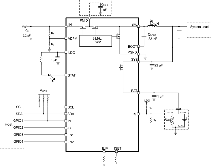
10.2 Typical Application
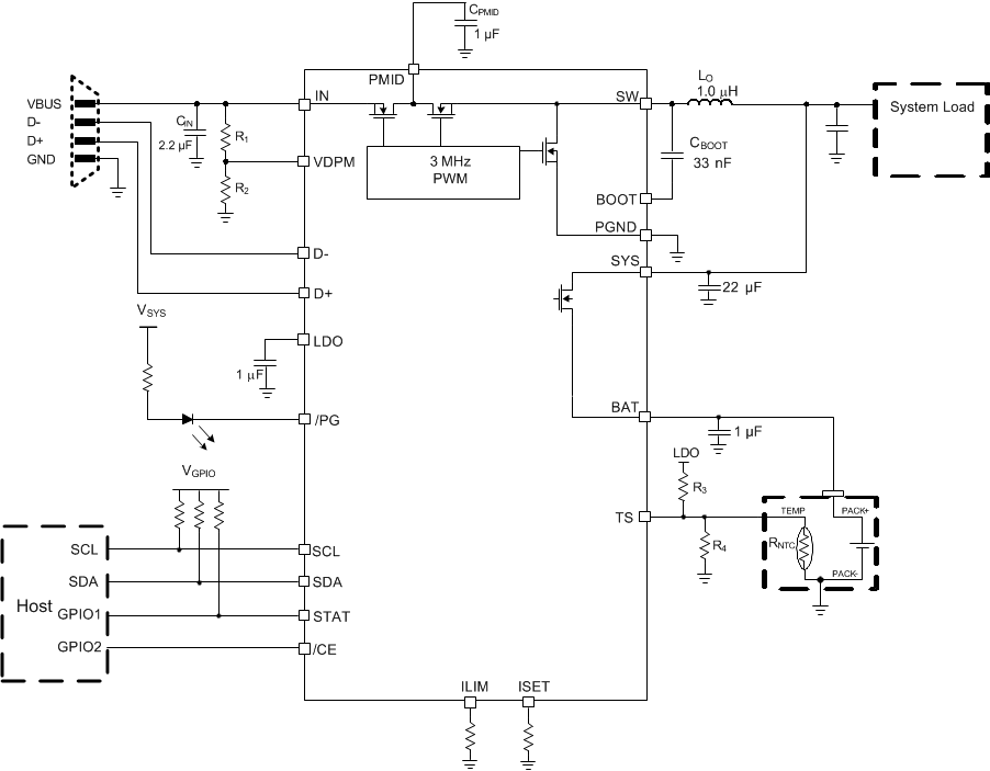 Figure 29. bq24251 Typical Application Circuit
10.2.1 Design Requirements
Use the following typical application design procedure to select external components values for the bq24251 device.
Table 5. Design Parameters
| SPECIFICATION | TEST CONDITION | MIN | TYP | MAX | UNIT |
|---|---|---|---|---|---|
| Input DC voltage, VIN | Recommended input voltage range | 4.35 | 10.5 | V | |
| Input current | Recommended input current range | 2 | A | ||
| Charge current | Fast charge current range | 0.5 | 2 | A | |
| Output regulation voltage | Standalone mode or I2C default mode | 4.2 | V | ||
| Output regulation voltage | I2C host mode: operating in voltage regulation, programmable range | 3.5 | 4.44 | V | |
| LDO | LDO output voltage | 4.9 | V |
10.2.2 Detailed Design Procedure
10.2.2.1 Inductor Selection
The inductor selection depends on the application requirements. The bq24250 is designed to operate at around 1 µH. The value will have an effect on efficiency, and the ripple requirements, stability of the charger, package size, and DCR of the inductor. The 1-μH inductor provides a good tradeoff between size and efficiency and ripple.
Once the inductance has been selected, the peak current is needed in order to choose the saturation current rating of the inductor. Make sure that the saturation current is always greater than or equal to the calculated IPEAK. The following equation can be used to calculate the current ripple:
Then use current ripple to calculate the peak current as follows:
In this design example, the regulation voltage is set to 4.2 V, the input voltage is 5 V and the inductance is selected to be 1-µH. The maximum charge current that can be used in this application is 1A and can be set by I2C command. The peak current is needed in order to choose the saturation current rating of the inductor. Using equation 6 and 7, ΔIL is calculated to be 0.224 A and the inductor peak current is 1.112 A. A 1-µF BAT cap is needed and 22-µF SYS cap is needed on the system trace.
The default settings for external fast charge current and external setting of current limit are chosen to be IFC=500 mA and ILIM=1 A. RISET and RILIM need to be calculated using equation 1 and 2 in the data sheet.
The fast charge current resistor (RISET) can be set as follows:
RISET=250/0.5A=500Ω
The input current limit resistor (RILIM) can be set as follows:
RILIM= 270/1A=270Ω
The external settings of VIN_DPM can be designed by calculating R1 and R2 according to Equation 3 in this data sheet and the typical application circuit. VIN_DPM should be chosen first along with R1. VIN_DPM is chosen to be 4.48 V and R1 is set to 274 KΩ in this design example. Using equation 3, the value of R2 is calculated to be 100 KΩ.
In this design example, the application needs to be JEITA compliant. Thus, TCOLD must be 0°C and THOT must be 60°C. If an NTC resistor is chosen such that the beta is 4500K and the nominal resistance is 13 KΩ, the calculated R3 and R4 values are 5 KΩ and 8.8 KΩ respectively. These results are obtained from Equation 4 and Equation 5 in this data sheet.
10.2.3 Application Curves
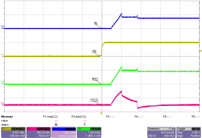
| VBAT = 3.8 V | ICHG = 1 A | |
| ISYS = 0 A | ILIM = 1.5 A |
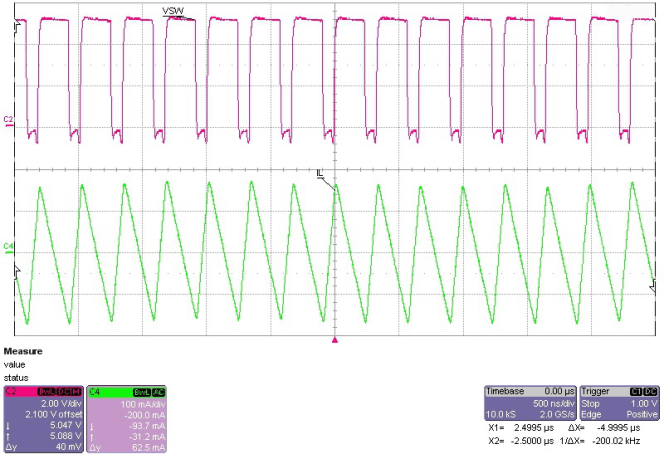
| VBAT = 3.3 V | ICHG = 1 A | VIN = 5.2 V |
| ISYS = 0 A |
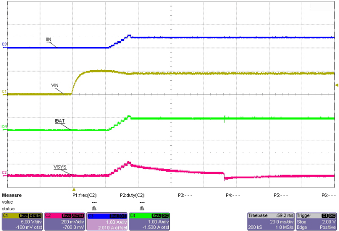
| VBAT = 3.6 V | ICHG = 2 A | VDPM = 4.36 V |
| ISYS = 0 A | ILIM = 0.5 A |
11 Power Supply Recommendations
12 Layout
12.1 Layout Guidelines
- Place the BOOT, PMID, IN, BAT, and LDO capacitors as close as possible to the IC for optimal performance.
- Connect the inductor as close as possible to the SW pin, and the SYS/CSIN cap as close as possible to the inductor minimizing noise in the path.
- Place a 1-μF PMID capacitor as close as possible to the PMID and PGND pins, making the high frequency current loop area as small as possible.
- The local bypass capacitor from SYS/CSIN to GND must be connected between the SYS/CSIN pin and PGND of the IC. This minimizes the current path loop area from the SW pin through the LC filter and back to the PGND pin.
- Place all decoupling capacitors close to their respective IC pins and as close as possible to PGND (do not place components such that routing interrupts power-stage currents). All small control signals must be routed away from the high-current paths.
- To reduce noise coupling, use a ground plane if possible, to isolate the noisy traces from spreading its noise all over the board. Put vias inside the PGND pads for the IC.
- The high-current charge paths into IN, Micro-USB, BAT, SYS/CSIN, and from the SW pins must be sized appropriately for the maximum charge current to avoid voltage drops in these traces.
- For high-current applications, the balls for the power paths must be connected to as much copper in the board as possible. This allows better thermal performance because the board conducts heat away from the IC.
12.2 Layout Example
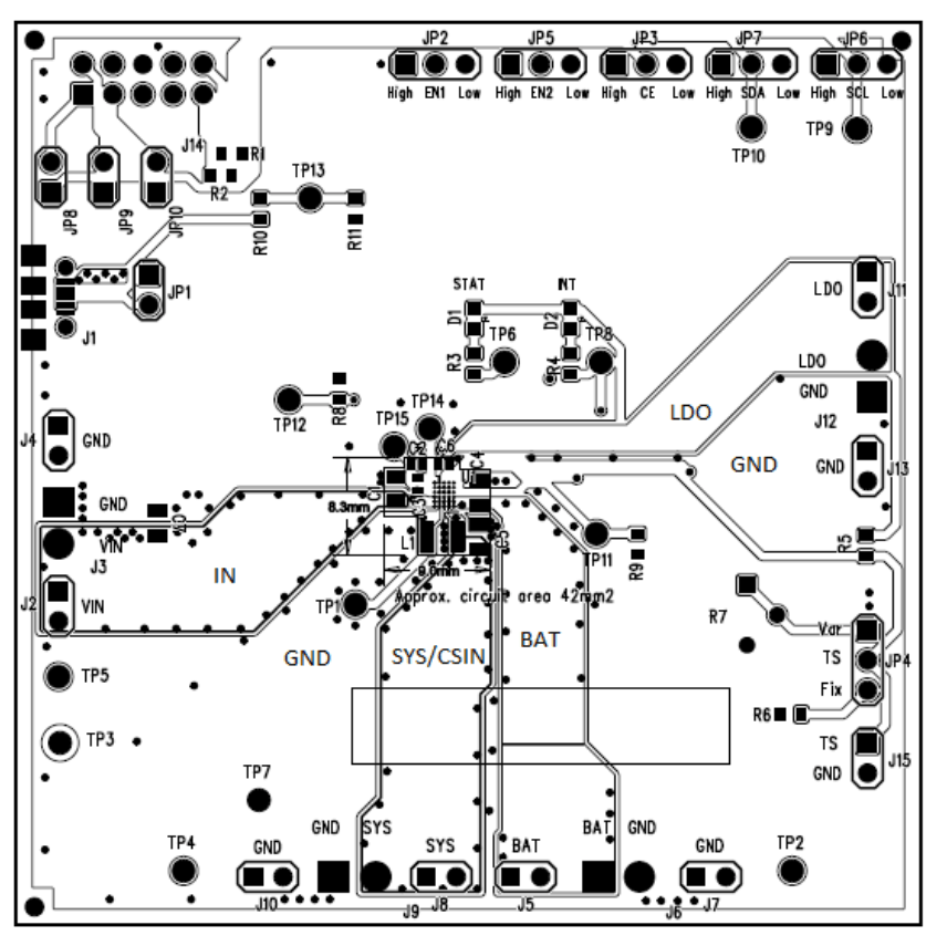 Figure 34. Recommended bq2425x PCB Layout for DSBGA Package
12.3 Thermal Considerations
During the charging process, to prevent overheat of the chip, bq2425x monitors the junction temperature, TJ, of the die and begins to taper down the charge current once TJ reaches the thermal regulation threshold, TREG. The charge current is reduced when the junction temperature increases above TREG. Once the charge current is reduced, the system current is reduced while the battery supplements the load to supply the system. This may cause a thermal shutdown of the IC if the die temperature rises too. At any state, if TJ exceeds TSHTDWN, bq2425x suspends charging and disables the buck converter. During thermal shutdown mode, PWM is turned off, all safety timers are suspended, and a single 256μs pulse is sent on the STAT and INT outputs and the FAULT/STAT bits of the status registers are updated in the I2C. A new charging cycle begins when TJ falls below TSHTDWN by approximately 10°C.
13 器件和文档支持
13.1 相关链接
下面的表格列出了快速访问链接。类别包括技术文档、支持与社区资源、工具和软件,以及申请样片或购买产品的快速链接。
13.2 商标
All trademarks are the property of their respective owners.
13.3 静电放电警告

这些装置包含有限的内置 ESD 保护。 存储或装卸时,应将导线一起截短或将装置放置于导电泡棉中,以防止 MOS 门极遭受静电损伤。
13.4 Glossary
SLYZ022 — TI Glossary.
This glossary lists and explains terms, acronyms, and definitions.
重要声明
德州仪器(TI) 及其下属子公司有权根据 JESD46 最新标准, 对所提供的产品和服务进行更正、修改、增强、改进或其它更改, 并有权根据 JESD48最新标准中止提供任何产品和服务。客户在下订单前应获取最新的相关信息, 并验证这些信息是否完整且是最新的。所有产品的销售都遵循在订单确认时所提供的TI 销售条款与条件。
TI 保证其所销售的组件的性能符合产品销售时 TI 半导体产品销售条件与条款的适用规范。仅在 TI 保证的范围内,且 TI 认为有必要时才会使用测试或其它质量控制技术。除非适用法律做出了硬性规定,否则没有必要对每种组件的所有参数进行测试。
TI 对应用帮助或客户产品设计不承担任何义务。客户应对其使用 TI 组件的产品和应用自行负责。为尽量减小与客户产品和应用相关的风险,客户应提供充分的设计与操作安全措施。
TI 不对任何 TI 专利权、版权、屏蔽作品权或其它与使用了 TI 组件或服务的组合设备、机器或流程相关的 TI 知识产权中授予 的直接或隐含权限作出任何保证或解释。TI所发布的与第三方产品或服务有关的信息,不能构成从 TI 获得使用这些产品或服 务的许可、授权、或认可。使用此类信息可能需要获得第三方的专利权或其它知识产权方面的许可,或是 TI 的专利权或其它知识产权方面的许可。
对于 TI 的产品手册或数据表中 TI 信息的重要部分,仅在没有对内容进行任何篡改且带有相关授权、条件、限制和声明的情况 下才允许进行复制。TI 对此类篡改过的文件不承担任何责任或义务。复制第三方的信息可能需要服从额外的限制条件。
在转售 TI 组件或服务时,如果对该组件或服务参数的陈述与 TI 标明的参数相比存在差异或虚假成分,则会失去相关 TI 组件或服务的所有明示或暗示授权,且这是不正当的、欺诈性商业行为。TI 对任何此类虚假陈述均不承担任何责任或义务。
客户认可并同意,尽管任何应用相关信息或支持仍可能由 TI 提供,但他们将独力负责满足与其产品及在其应用中使用 TI 产品相关的所有法律、法规和安全相关要求。客户声明并同意,他们具备制定与实施安全措施所需的全部专业技术和知识,可预见故障的危险后果、监测故障及其后果、降低有可能造成人身伤害的故障的发生机率并采取适当的补救措施。客户将全额赔偿因 在此类安全关键应用中使用任何 TI 组件而对 TI及其代理造成的任何损失。
在某些场合中,为了推进安全相关应用有可能对 TI 组件进行特别的促销。TI 的目标是利用此类组件帮助客户设计和创立其特有的可满足适用的功能安全性标准和要求的终端产品解决方案。尽管如此,此类组件仍然服从这些条款。
TI 组件未获得用于 FDA Class III(或类似的生命攸关医疗设备)的授权许可,除非各方授权官员已经达成了专门管控此类使 用的特别协议。
只有那些 TI 特别注明属于军用等级或“增强型塑料”的 TI 组件才是设计或专门用于军事/航空应用或环境的。购买者认可并同 意,对并非指定面向军事或航空航天用途的 TI组件进行军事或航空航天方面的应用,其风险由客户单独承担,并且由客户独 力负责满足与此类使用相关的所有法律和法规要求。
TI 已明确指定符合 ISO/TS16949 要求的产品,这些产品主要用于汽车。在任何情况下,因使用非指定产品而无法达到 ISO/TS16949要求,TI不承担任何责任。
产品
- 数字音频: www.ti.com.cn/audio
- 放大器和线性器件: www.ti.com.cn/amplifiers
- 数据转换器: www.ti.com.cn/dataconverters
- DLP® 产品: www.dlp.com
- DSP - 数字信号处理器: www.ti.com.cn/dsp
- 时钟和计时器: www.ti.com.cn/clockandtimers
- 接口: www.ti.com.cn/interface
- 逻辑: www.ti.com.cn/logic
- 电源管理: www.ti.com.cn/power
- 微控制器 (MCU): www.ti.com.cn/microcontrollers
- RFID 系统: www.ti.com.cn/rfidsys
- OMAP应用处理器: www.ti.com/omap
- 无线连通性: www.ti.com.cn/wirelessconnectivity
应用
- 通信与电信: www.ti.com.cn/telecom
- 计算机及周边: www.ti.com.cn/computer
- 消费电子: www.ti.com/consumer-apps
- 能源: www.ti.com/energy
- 工业应用: www.ti.com.cn/industrial
- 医疗电子: www.ti.com.cn/medical
- 安防应用: www.ti.com.cn/security
- 汽车电子: www.ti.com.cn/automotive
- 视频和影像: www.ti.com.cn/video
德州仪器在线技术支持社区: www.deyisupport.com
邮寄地址: 上海市浦东新区世纪大道1568 号,中建大厦32 楼邮政编码: 200122
Copyright© 2016, 德州仪器半导体技术(上海)有限公司


