-
DAC128S085 12-Bit Micro-Power OCTAL Digital-to-Analog Converter With Rail-to-Rail Outputs
- 1 Features
- 2 Applications
- 3 Description
- 4 Revision History
- 5 Description (continued)
- 6 Pin Configuration and Functions
- 7 Specifications
- 8 Detailed Description
- 9 Application and Implementation
- 10Power Supply Recommendations
- 11Layout
- 12Device and Documentation Support
- 13Mechanical, Packaging, and Orderable Information
- IMPORTANT NOTICE
DAC128S085 12-Bit Micro-Power OCTAL Digital-to-Analog Converter With Rail-to-Rail Outputs
1 Features
- Ensured Monotonicity
- Low Power Operation
- Rail-to-Rail Voltage Output
- Daisy-Chain Capability
- Power-on Reset to 0 V
- Simultaneous Output Updating
- Individual Channel Power-Down Capability
- Wide Power Supply Range (2.7 V to 5.5 V)
- Dual Reference Voltages With Range of 0.5 V to VA
- Operating Temperature Range of −40°C to 125°C
- Smallest Package in the Industry
- Resolution 12 Bits
- INL ±8 LSB (Maximum)
- DNL 0.75 / −0.4 LSB (Maximum)
- Settling Time 8.5 μs (Maximum)
- Zero Code Error 15 mV (Maximum)
- Full-Scale Error −0.75 %FSR (Maximum)
- Supply Power
- 1.95 mW (3 V) / 4.85 mW (5 V) Typical
- Power Down 0.3 μW (3 V) / 1 μW (5 V) Typical
2 Applications
- Battery-Powered Instruments
- Digital Gain and Offset Adjustment
- Programmable Voltage and Current Sources
- Programmable Attenuators
- Voltage Reference for ADCs
- Sensor Supply Voltage
- Range Detectors
3 Description
The DAC128S085 is a full-featured, general-purpose OCTAL 12-bit voltage-output digital-to-analog converter (DAC) that can operate from a single 2.7-V to 5.5-V supply and consumes 1.95 mW at 3 V and 4.85 mW at 5 V. The DAC128S085 is packaged in a 16-lead WQFN package and a 16-lead TSSOP package. The WQFN package makes the DAC128S085 the smallest OCTAL DAC in its class. The on-chip output amplifiers allow rail-to-rail output swing, and the 3-wire serial interface operates at clock rates up to 40 MHz over the entire supply voltage range. Competitive devices are limited to 25-MHz clock rates at supply voltages in the 2.7-V to 3.6-V range. The serial interface is compatible with standard SPI™, QSPI, MICROWIRE, and DSP interfaces. The DAC128S085 also offers daisy-chain operation, where an unlimited number of DAC128S085s can be updated simultaneously using a single serial interface.
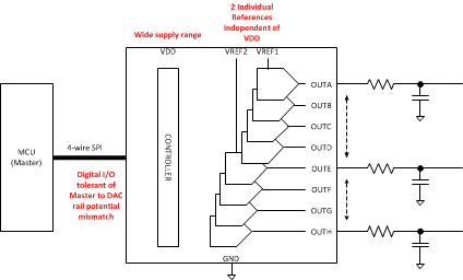
There are two references for the DAC128S085. One reference input serves channels A through D, while the other reference serves channels E through H. Each reference can be set independently between 0.5 V and VA, providing the widest possible output dynamic range. The DAC128S085 has a 16-bit input shift register that controls the mode of operation, the power-down condition, and the register/output value of the DAC channels. All eight DAC outputs can be updated simultaneously or individually.
Device Information(1)
| PART NUMBER | PACKAGE | BODY SIZE (NOM) |
|---|---|---|
| DAC128S085 | TSSOP (16) | 5.00 mm × 4.4 mm |
| WQFN (16) | 4.00 mm × 4.00 mm |
- For all available packages, see the orderable addendum at the end of the datasheet.
Simplified Schematic
4 Revision History
Changes from G Revision (January 2015) to H Revision
- Switched WQFN and TSSOP pinouts to their correct titles Go
- Re-drew TSSOP pinout as a square to better reflect mechanical packaging drawings Go
Changes from F Revision (March 2013) to G Revision
- Added Pin Configuration and Functions section, ESD Ratings table, Feature Description section, Device Functional Modes, Application and Implementation section, Power Supply Recommendations section, Layout section, Device and Documentation Support section, and Mechanical, Packaging, and Orderable Information section Go
Changes from E Revision (March 2013) to F Revision
- Changed layout of National Data Sheet to TI formatGo
5 Description (continued)
A power-on reset circuit ensures that the DAC outputs power up to zero volts and remain there until there is a valid write to the device. The power-down feature of the DAC128S085 allows each DAC to be independently powered with three different termination options. With all the DAC channels powered down, power consumption reduces to less than 0.3 µW at 3 V and less than 1 µW at 5 V. The low power consumption and small packages of the DAC128S085 make it an excellent choice for use in battery-operated equipment.
The DAC128S085 is one of a family of pin-compatible DACs, including the 8-bit DAC088S085 and the 10-bit DAC108S085. All three parts are offered with the same pinout, allowing system designers to select a resolution appropriate for their application without redesigning their printed circuit board. The DAC128S085 operates over the extended industrial temperature range of −40°C to 125°C.
6 Pin Configuration and Functions
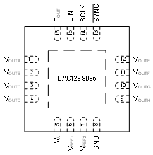
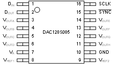
Pin Functions
7 Specifications
7.1 Absolute Maximum Ratings
over operating free-air temperature range (unless otherwise noted)(1)(1)| MIN | MAX | UNIT | ||
|---|---|---|---|---|
| Supply Voltage, VA | 6.5 | V | ||
| Voltage on any Input Pin | −0.3 | 6.5 | V | |
| Input Current at Any Pin(2) | 10 | mA | ||
| Package Input Current(2) | 30 | mA | ||
| Power Consumption at TA = 25°C | See (3) | |||
| Junction Temperature | 150 | °C | ||
| Storage Temperature, Tstg | −65 | 150 | °C | |
7.2 ESD Ratings
| VALUE | UNIT | |||
|---|---|---|---|---|
| V(ESD) | Electrostatic discharge | Human body model (HBM), per ANSI/ESDA/JEDEC JS-001(1) | ±2500 | V |
| Charged-device model (CDM), per JEDEC specification JESD22-C101(2) | ±1000 | |||
| Machine Model | ±250 | |||
7.3 Recommended Operating Conditions
over operating free-air temperature range (unless otherwise noted)| MIN | MAX | UNIT | ||
|---|---|---|---|---|
| Operating Temperature Range | −40 ≤ TA ≤ +125 | °C | ||
| Supply Voltage, VA | 2.7 | 5.5 | V | |
| Reference Voltage, VREF1,2 | 0.5 | VA | V | |
| Digital Input Voltage(1) | 0.0 | 5.5 | V | |
| Output Load | 0 | 1500 | pF | |
| SCLK Frequency | 40 | MHz | ||
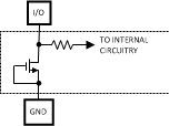
7.4 Thermal Information
| THERMAL METRIC(1) | DAC128S085 | UNIT | ||
|---|---|---|---|---|
| PW (TSSOP) | RGH (WQFN) | |||
| 16 PINS | 16 PINS | |||
| RθJA | Junction-to-ambient thermal resistance | 98 | 34 | °C/W |
| RθJA | Junction-to-ambient thermal resistance | 31 | 25 | |
| RθJA | Junction-to-ambient thermal resistance | 43 | 11 | |
| φJT | Junction-to-top characterization parameter | 2 | 0.2 | |
| φJB | Junction-to-board characterization parameter | 43 | 11 | |
7.5 Electrical Characteristics
The following specifications apply for VA = 2.7 V to 5.5 V, VREF1 = VREF2 = VA, CL = 200 pF to GND, fSCLK = 30 MHz, input code range 48 to 4047. All limits are at TA = 25°C, unless otherwise specified.| PARAMETER | TEST CONDITIONS | MIN(2) | TYP | MAX(2) | UNIT | ||
|---|---|---|---|---|---|---|---|
| STATIC PERFORMANCE | |||||||
| Resolution | TMIN ≤ TA ≤ TMAX | 12 | Bits | ||||
| Monotonicity | TMIN ≤ TA ≤ TMAX | 12 | Bits | ||||
| INL | Integral Non-Linearity | ±2 | LSB | ||||
| TMIN ≤ TA ≤ TMAX | ±8 | ||||||
| DNL | Differential Non-Linearity | 0.15 | LSB | ||||
| TMIN ≤ TA ≤ TMAX | 0.75 | ||||||
| −0.09 | LSB | ||||||
| TMIN ≤ TA ≤ TMAX | −0.4 | ||||||
| ZE | Zero Code Error | IOUT = 0 | +5 | mV | |||
| TMIN ≤ TA ≤ TMAX | 15 | ||||||
| FSE | Full-Scale Error | IOUT = 0 | −0.1% | FSR | |||
| TMIN ≤ TA ≤ TMAX | −0.75% | ||||||
| GE | Gain Error | −0.2% | FSR | ||||
| TMIN ≤ TA ≤ TMAX | −1 % | ||||||
| ZCED | Zero Code Error Drift | −20 | µV/°C | ||||
| TC GE | Gain Error Tempco | −1 | ppm/°C | ||||
| OUTPUT CHARACTERISTICS | |||||||
| Output Voltage Range | TMIN ≤ TA ≤ TMAX | 0 | VREF1,2 | V | |||
| IOZ | High-Impedance Output Leakage Current(3) |
TMIN ≤ TA ≤ TMAX | ±1 | µA | |||
| ZCO | Zero Code Output | VA = 3 V, IOUT = 200 µA | 10 | mV | |||
| VA = 3 V, IOUT = 1 mA | 45 | mV | |||||
| VA = 5 V, IOUT = 200 µA | 8 | mV | |||||
| VA = 5 V, IOUT = 1 mA | 34 | mV | |||||
| FSO | Full Scale Output | VA = 3 V, IOUT = 200 µA | 2.984 | V | |||
| VA = 3 V, IOUT = 1 mA | 2.933 | V | |||||
| VA = 5 V, IOUT = 200 µA | 4.987 | V | |||||
| VA = 5 V, IOUT = 1 mA | 4.955 | V | |||||
| IOS | Output Short Circuit Current (source)(4) | VA = 3 V, VOUT = 0 V, Input Code = FFFh |
−50 | mA | |||
| VA = 5 V, VOUT = 0 V, Input Code = FFFh |
−60 | mA | |||||
| IOS | Output Short Circuit Current (sink)(4) | VA = 3 V, VOUT = 3 V, Input Code = 000h |
50 | mA | |||
| VA = 5 V, VOUT = 5 V, Input Code = 000h |
70 | mA | |||||
| IO | Continuous Output Current per channel(3) | TA = 105°C TMIN ≤ TA ≤ TMAX |
10 | mA | |||
| TA = 125°C TMIN ≤ TA ≤ TMAX |
6.5 | mA | |||||
| CL | Maximum Load Capacitance | RL = ∞ | 1500 | pF | |||
| RL = 2 kΩ | 1500 | pF | |||||
| ZOUT | DC Output Impedance | 8 | Ω | ||||
| REFERENCE INPUT CHARACTERISTICS | |||||||
| VREF1,2 | Input Range Minimum | 0.5 | V | ||||
| TMIN ≤ TA ≤ TMAX | 2.7 | ||||||
| Input Range Maximum | TMIN ≤ TA ≤ TMAX | VA | V | ||||
| Input Impedance | 30 | kΩ | |||||
| LOGIC INPUT CHARACTERISTICS | |||||||
| IIN | Input Current(3) | TMIN ≤ TA ≤ TMAX | ±1 | µA | |||
| VIL | Input Low Voltage | VA = 2.7 V to 3.6 V | 1 | V | |||
| TMIN ≤ TA ≤ TMAX | 0.6 | ||||||
| VA = 4.5 V to 5.5 V | 1.1 | V | |||||
| 0.8 | |||||||
| VIH | Input High Voltage | VA = 2.7 V to 3.6 V | 1.4 | V | |||
| TMIN ≤ TA ≤ TMAX | 2.1 | ||||||
| VA = 4.5 V to 5.5 V | 2 | V | |||||
| TMIN ≤ TA ≤ TMAX | 2.4 | ||||||
| CIN | Input Capacitance(3) | TMIN ≤ TA ≤ TMAX | 3 | pF | |||
| POWER REQUIREMENTS | |||||||
| VA | Supply Voltage Minimum | TMIN ≤ TA ≤ TMAX | 2.7 | V | |||
| Supply Voltage Maximum | TMIN ≤ TA ≤ TMAX | 5.5 | V | ||||
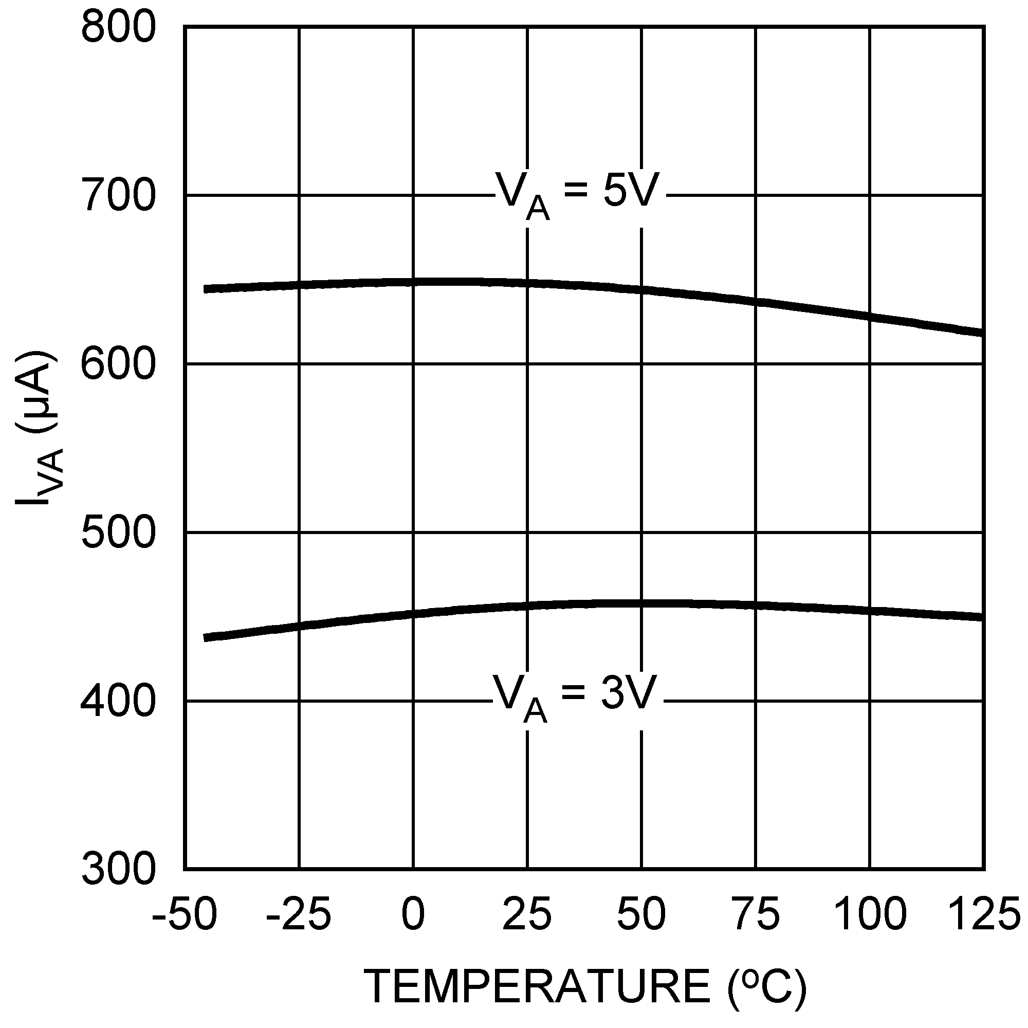
| IN | Normal Supply Current for supply pin VA | fSCLK = 30 MHz, output unloaded |
VA = 2.7 V to 3.6 V | 460 | µA | ||
| TMIN ≤ TA ≤ TMAX | 560 | ||||||
| VA = 4.5 V to 5.5 V | 650 | µA | |||||
| 830 | |||||||
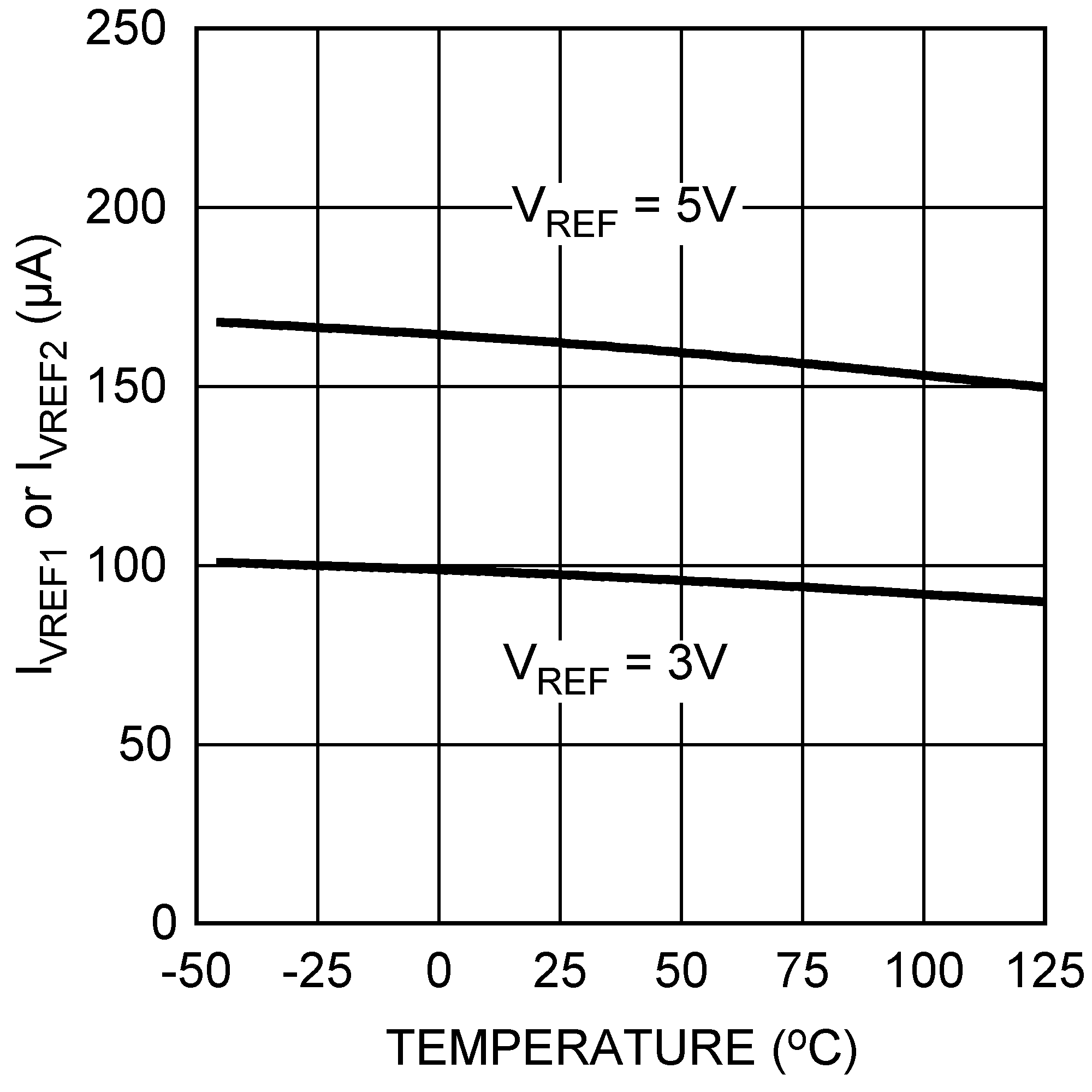
| Normal Supply Current for VREF1 or VREF2 | fSCLK = 30 MHz, output unloaded |
VA = 2.7 V to 3.6 V | 95 | µA | |||
| TMIN ≤ TA ≤ TMAX | 130 | ||||||
| VA = 4.5 V to 5.5 V | 160 | µA | |||||
| 220 | |||||||
| IST | Static Supply Current for supply pin VA | fSCLK = 0, output unloaded |
VA = 2.7 V to 3.6 V | 370 | µA | ||
| VA = 4.5 V to 5.5 V | 440 | µA | |||||
| Static Supply Current for VREF1 or VREF2 | fSCLK = 0, output unloaded |
VA = 2.7 V to 3.6 V | 95 | µA | |||
| VA = 4.5 V to 5.5 V | 160 | µA | |||||
| IPD | Total Power Down Supply Current for all PD Modes (3) |
fSCLK = 30 MHz, SYNC = VA and DIN = 0V after PD mode loaded | VA = 2.7 V to 3.6 V | 0.2 | µA | ||
| 1.5 | |||||||
| VA = 4.5 V to 5.5 V | 0.5 | µA | |||||
| TMIN ≤ TA ≤ TMAX | 3 | ||||||
| fSCLK = 0, SYNC = VA and DIN = 0V after PD mode loaded | VA = 2.7 V to 3.6 V | 0.1 | µA | ||||
| TMIN ≤ TA ≤ TMAX | 1 | ||||||
| VA = 4.5 V to 5.5 V | 0.2 | µA | |||||
| TMIN ≤ TA ≤ TMAX | 2 | ||||||
| PN | Total Power Consumption (output unloaded) | fSCLK = 30 MHz output unloaded |
VA = 2.7 V to 3.6 V | 1.95 | mW | ||
| TMIN ≤ TA ≤ TMAX | 3 | ||||||
| VA = 4.5 V to 5.5 V | 4.85 | mW | |||||
| TMIN ≤ TA ≤ TMAX | 7 | ||||||
| fSCLK = 0 output unloaded |
VA = 2.7 V to 3.6 V | 1.68 | mW | ||||
| VA = 4.5 V to 5.5 V | 3.80 | mW | |||||
| PPD | Total Power Consumption in all PD Modes, (3) |
fSCLK = 30 MHz, SYNC = VA and DIN = 0V after PD mode loaded | VA = 2.7 V to 3.6 V | 0.6 | µW | ||
| TMIN ≤ TA ≤ TMAX | 5.4 | ||||||
| VA = 4.5V to 5.5V | 2.5 | µW | |||||
| TMIN ≤ TA ≤ TMAX | 16.5 | ||||||
| fSCLK = 0, SYNC = VA and DIN = 0V after PD mode loaded | VA = 2.7 V to 3.6 V | 0.3 | µW | ||||
| TMIN ≤ TA ≤ TMAX | 3.6 | ||||||
| VA = 4.5 V to 5.5 V | 1 | µW | |||||
| TMIN ≤ TA ≤ TMAX | 11 | ||||||
7.6 AC and Timing Characteristics
The following specifications apply for VA = 2.7 V to 5.5 V, VREF1,2 = VA, CL = 200 pF to GND, fSCLK = 30 MHz, input code range 48 to 4047. All limits are at TA = 25°C, unless otherwise specified.| MIN(2) | NOM | MAX(2) | UNIT | ||||
|---|---|---|---|---|---|---|---|
| fSCLK | SCLK Frequency | 40 | MHz | ||||
| TMIN ≤ TA ≤ TMAX | 30 | ||||||
| ts | Output Voltage Settling Time (3) |
400h to C00h code change RL = 2 kΩ, CL = 200 pF |
6 | µs | |||
| TMIN ≤ TA ≤ TMAX | 8.5 | ||||||
| SR | Output Slew Rate | 1 | V/µs | ||||
| GI | Glitch Impulse | Code change from 800h to 7FFh | 40 | nV-sec | |||
| DF | Digital Feedthrough | 0.5 | nV-sec | ||||
| DC | Digital Crosstalk | 0.5 | nV-sec | ||||
| CROSS | DAC-to-DAC Crosstalk | 1 | nV-sec | ||||
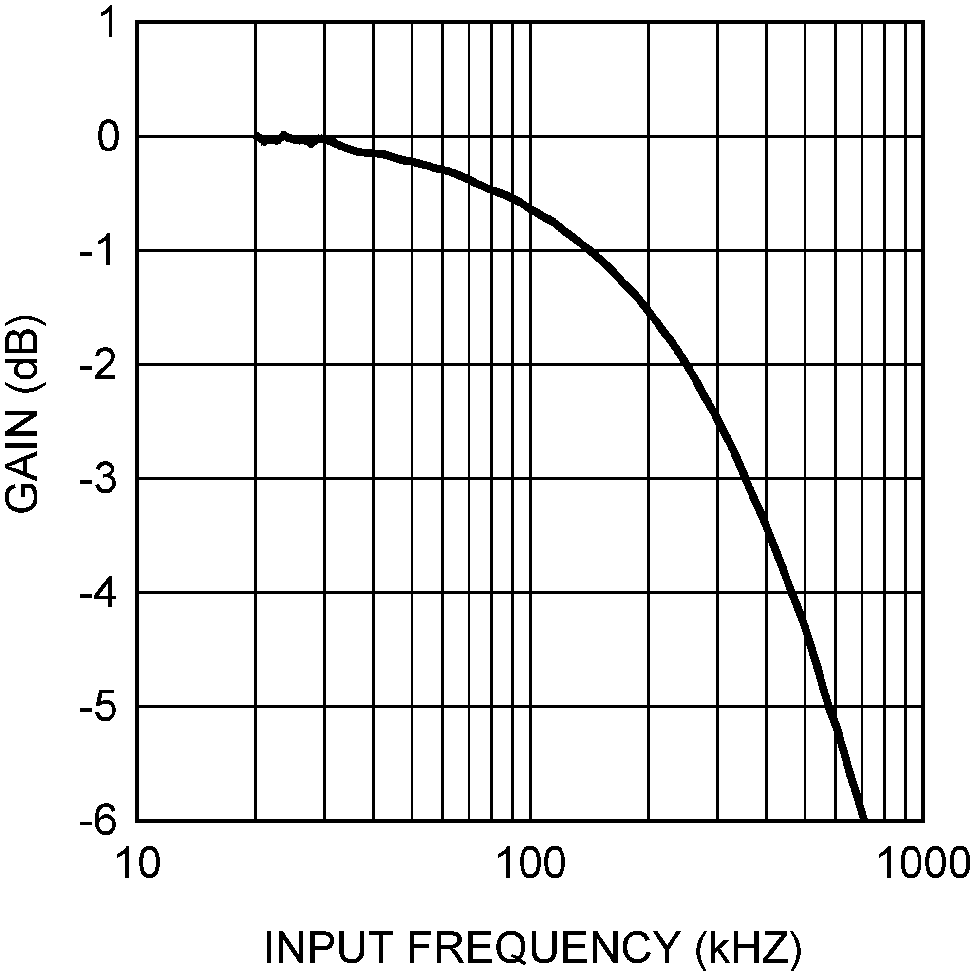
| MBW | Multiplying Bandwidth | VREF1,2 = 2.5 V ± 2 Vpp | 360 | kHz | |||
| THD+N | Total Harmonic Distortion Plus Noise | VREF1,2 = 2.5 V ± 0.5 Vpp 100 Hz < fIN < 20 kHz |
−80 | dB | |||
| ONSD | Output Noise Spectral Density | DAC Code = 800 h, 10 kHz | 40 | nV/sqrt (Hz) | |||
| ON | Output Noise | BW = 30 kHz | 14 | µV | |||
| tWU | Wake-Up Time | VA = 3 V | 3 | µsec | |||
| VA = 5 V | 20 | µsec | |||||
| 1/fSCLK | SCLK Cycle Time. See Figure 1 | 25 | ns | ||||
| TMIN ≤ TA ≤ TMAX | 33 | ||||||
| tCH | SCLK High time. See Figure 1 | 7 | ns | ||||
| TMIN ≤ TA ≤ TMAX | 10 | ||||||
| tCL | SCLK Low Time. See Figure 1 | 7 | ns | ||||
| TMIN ≤ TA ≤ TMAX | 10 | ||||||
| tSS | SYNC Set-up Time prior to SCLK Falling Edge. See Figure 1 | 3 | 1 / fSCLK - 3 | ns | |||
| TMIN ≤ TA ≤ TMAX | 10 | ||||||
| tDS | Data Set-Up Time prior to SCLK Falling Edge. See Figure 1 | 1 | ns | ||||
| TMIN ≤ TA ≤ TMAX | 2.5 | ||||||
| tDH | Data Hold Time after SCLK Falling Edge. See Figure 1 | 1 | ns | ||||
| TMIN ≤ TA ≤ TMAX | 2.5 | ||||||
| tSH | SYNC Hold Time after the 16th falling edge of SCLK. See Figure 1 | 0 | 1 / fSCLK - 3 | ns | |||
| TMIN ≤ TA ≤ TMAX | 3 | ||||||
| tSYNC | SYNC High Time. See Figure 1 | 5 | ns | ||||
| TMIN ≤ TA ≤ TMAX | 15 | ||||||
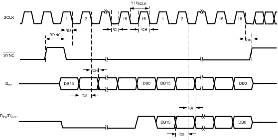 Figure 1. Serial Timing Diagram
7.7 Typical Characteristics
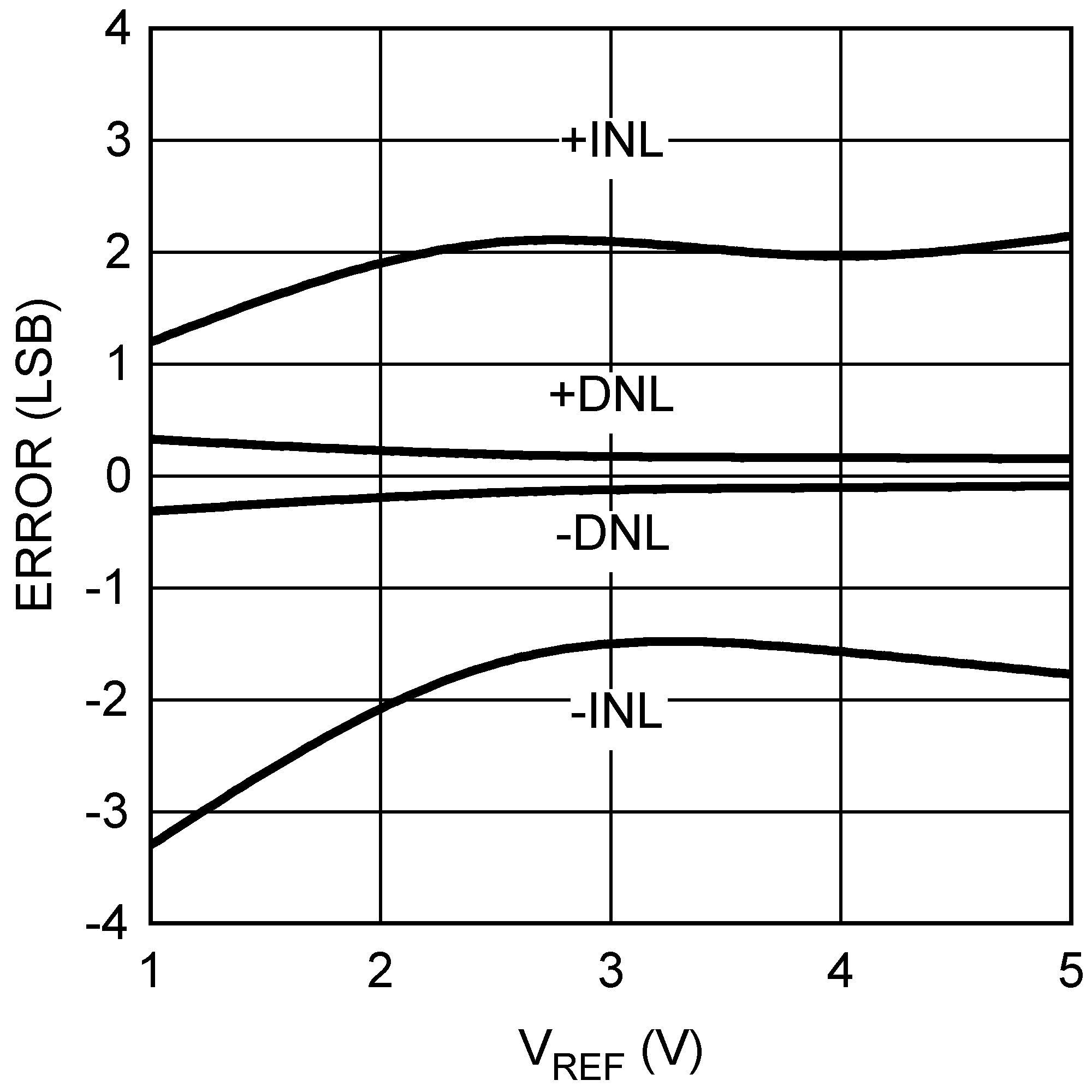
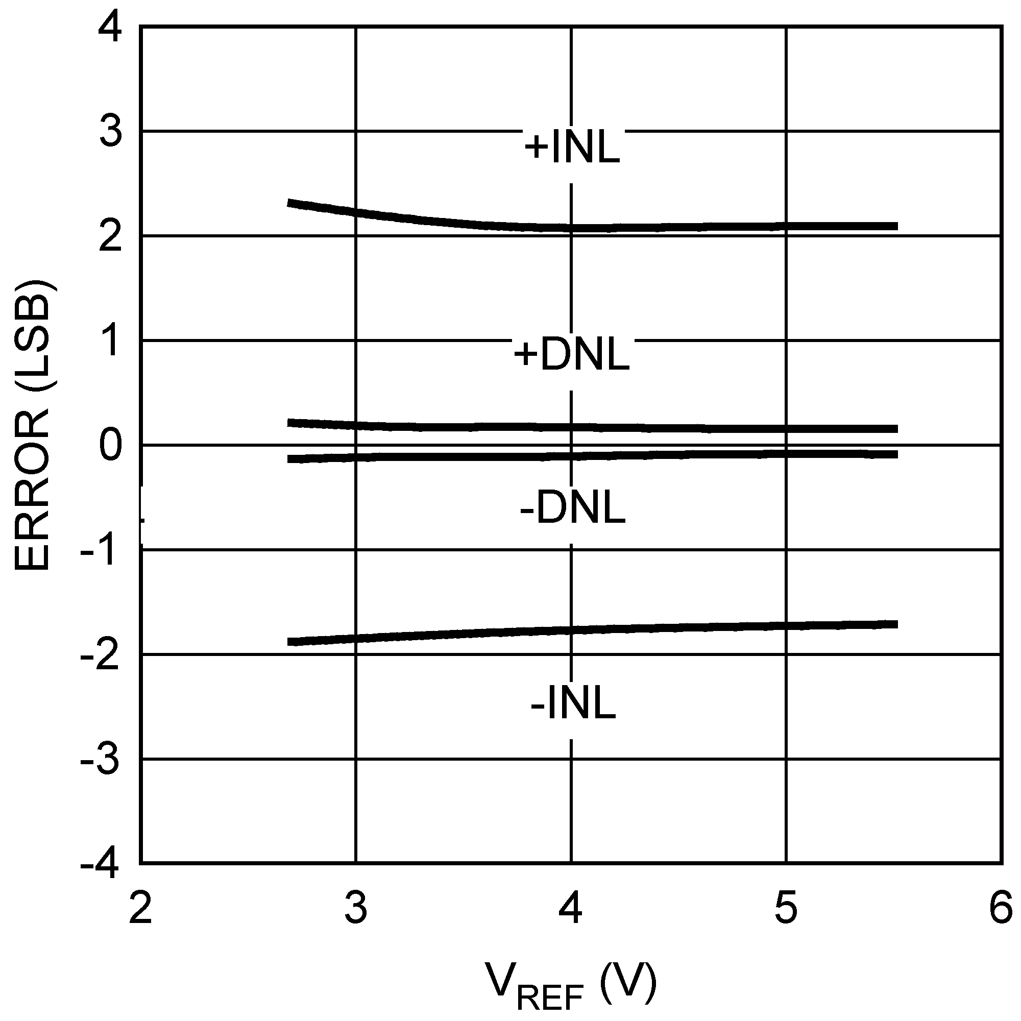
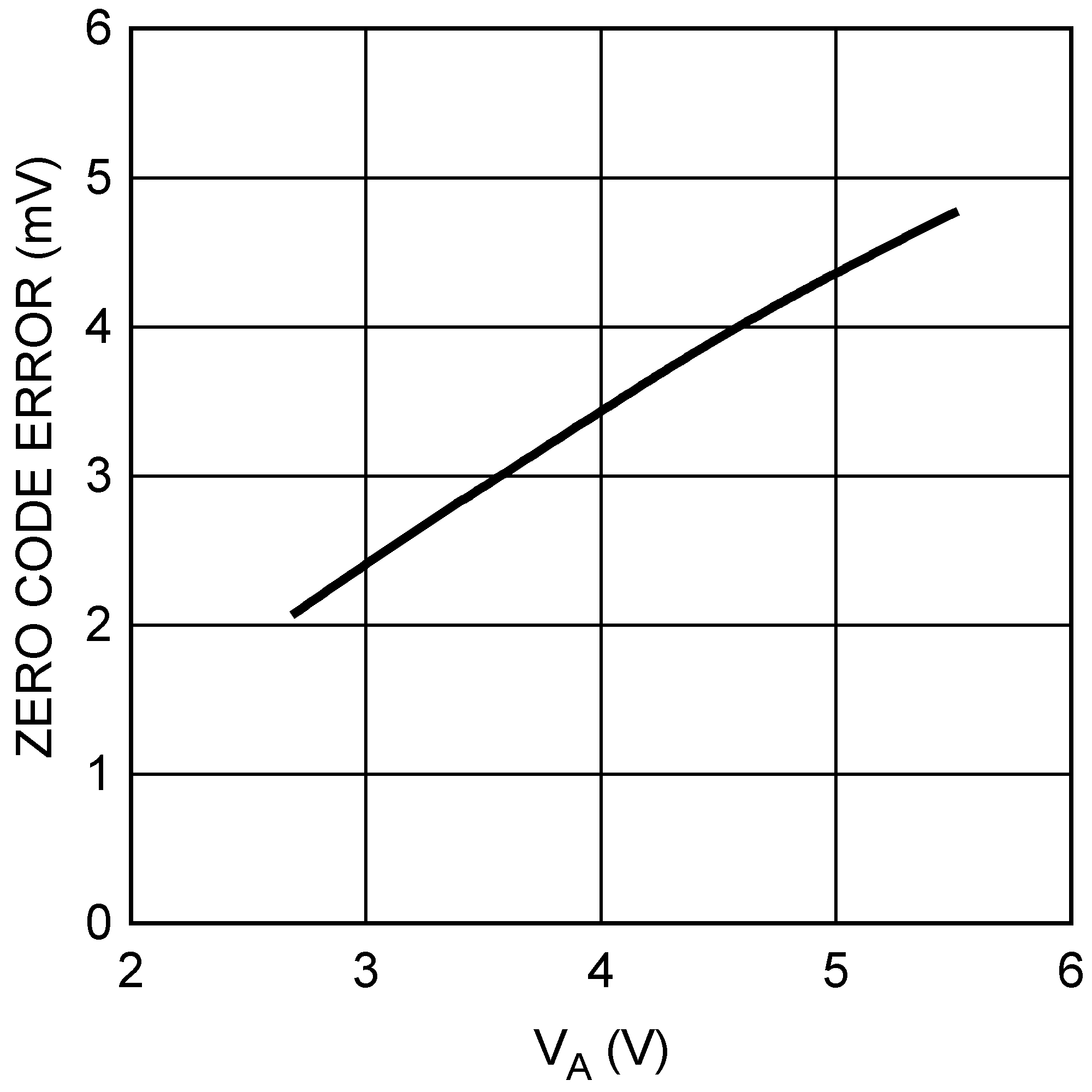
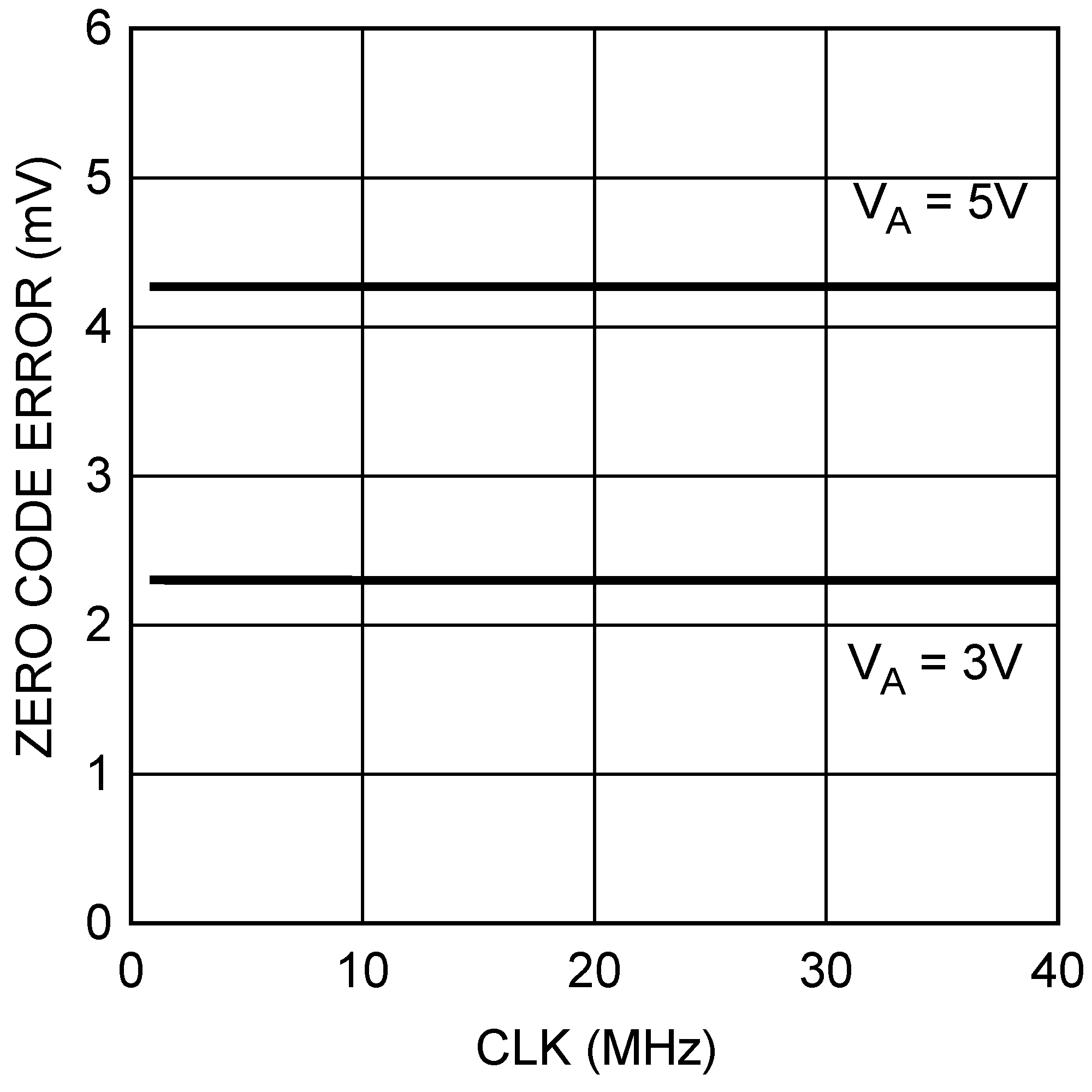
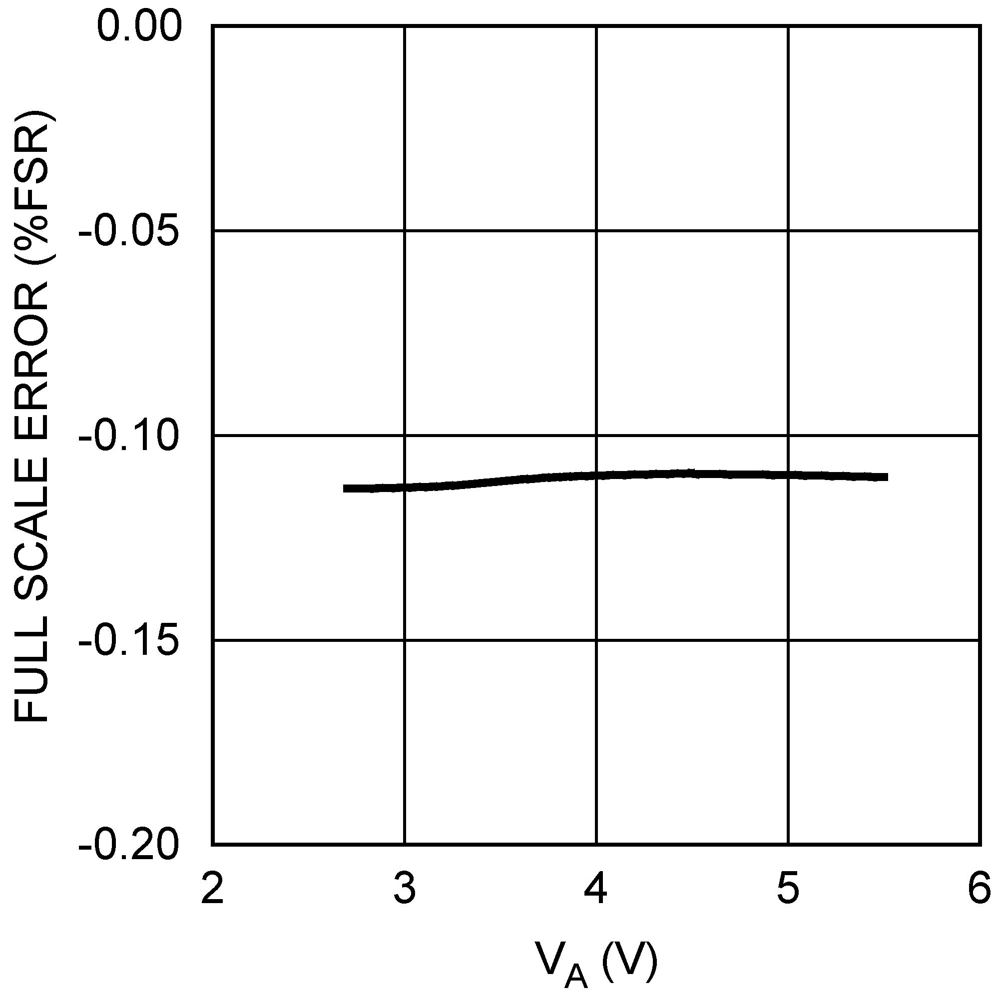
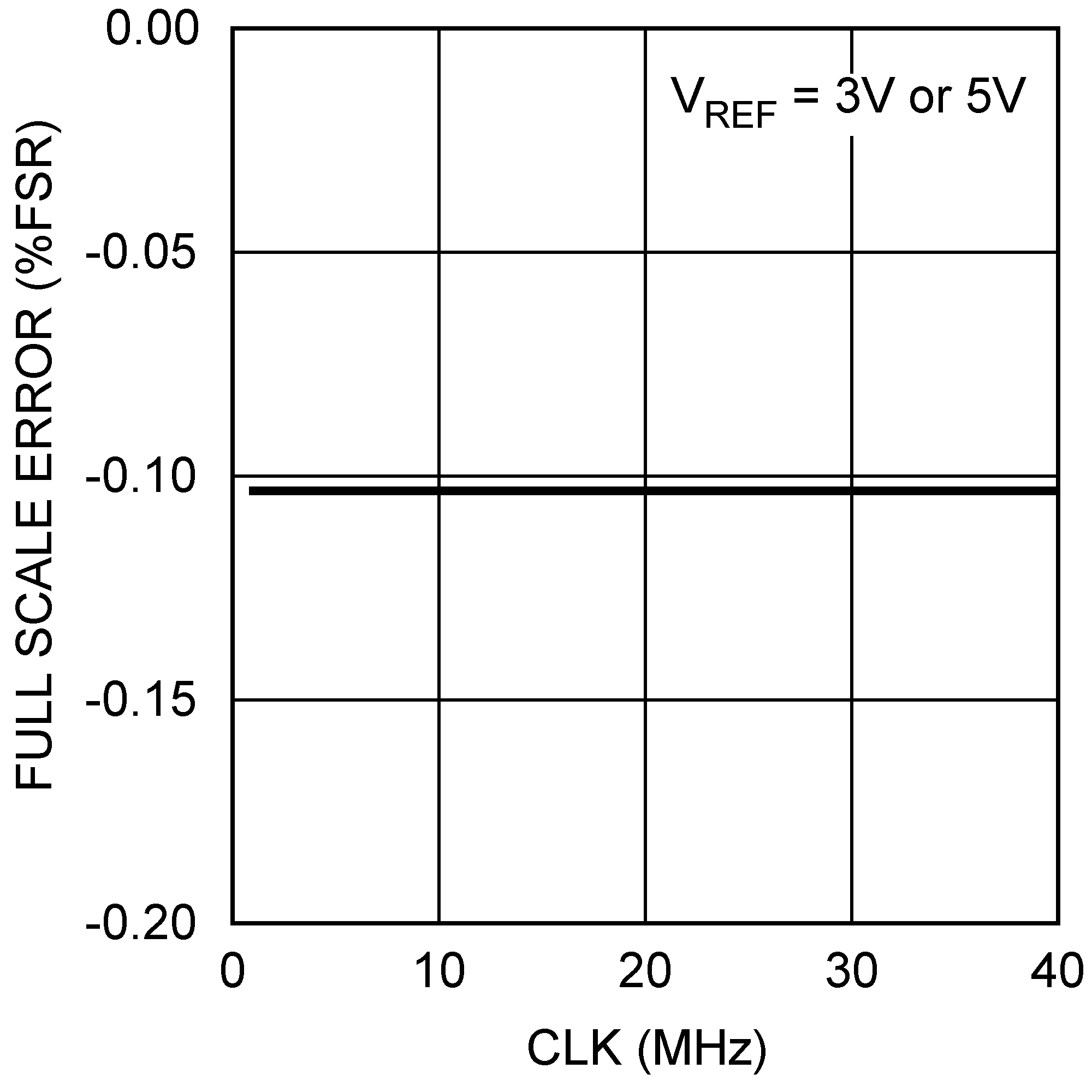
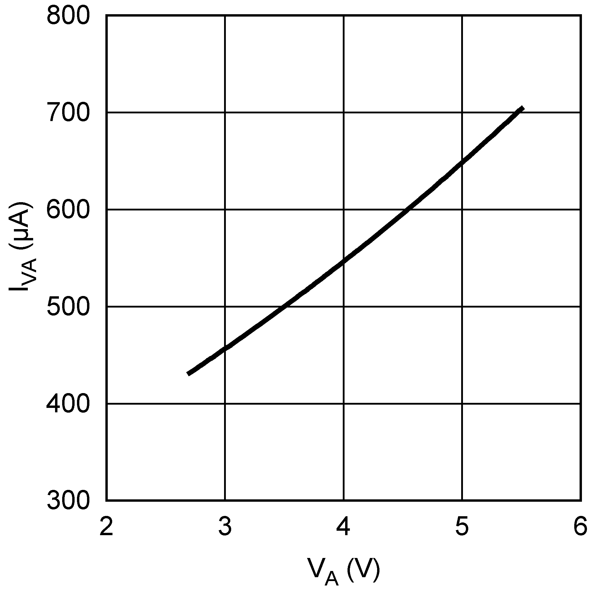
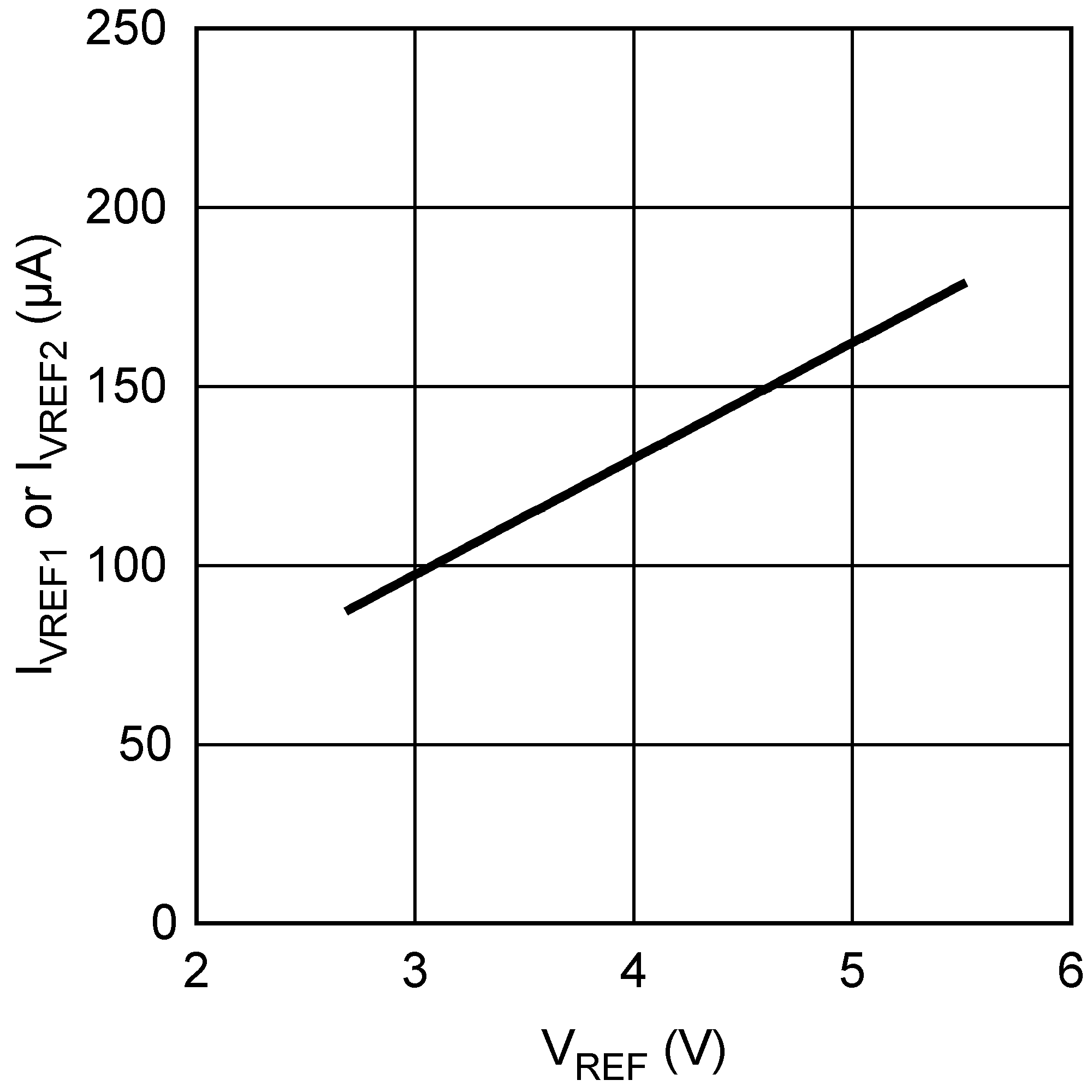
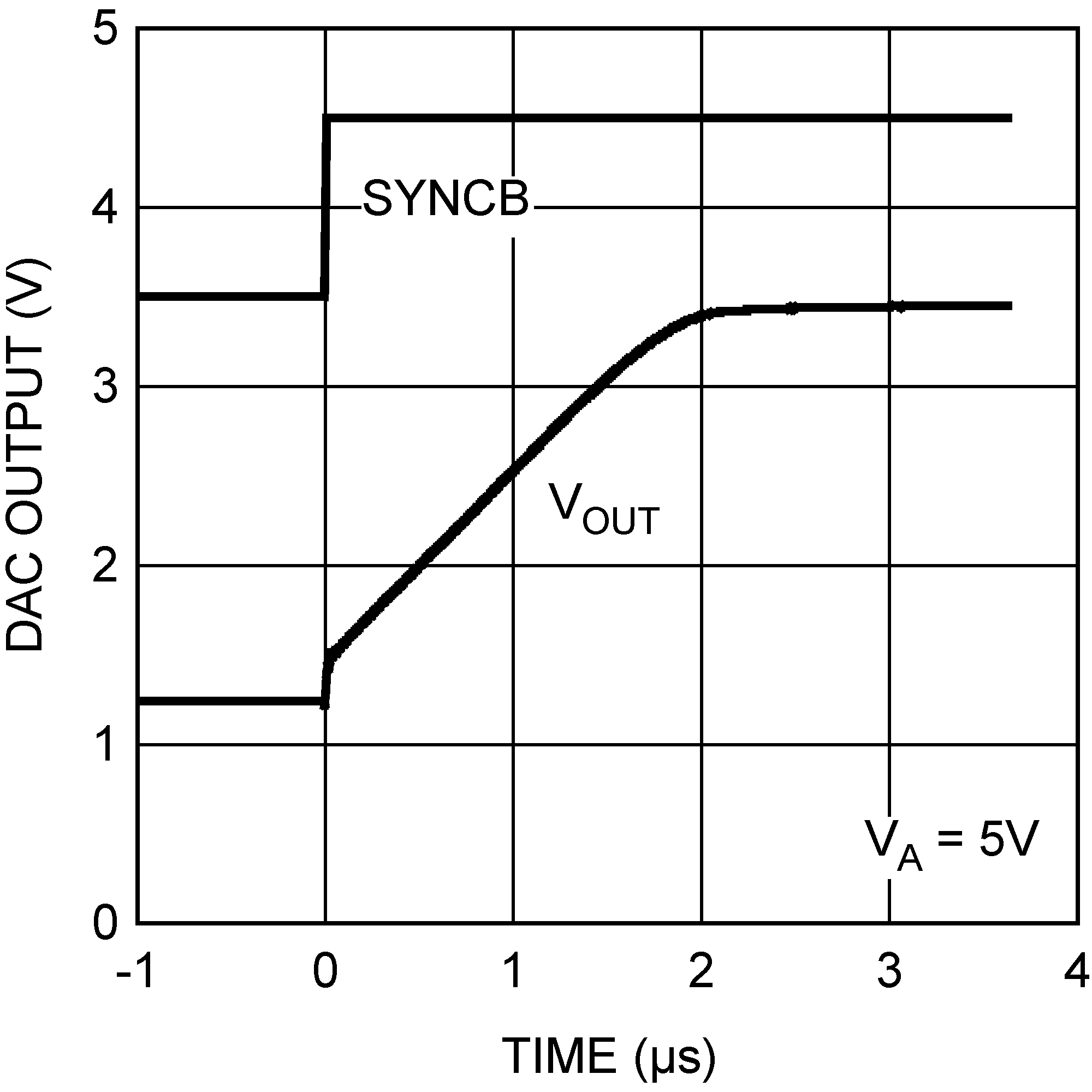
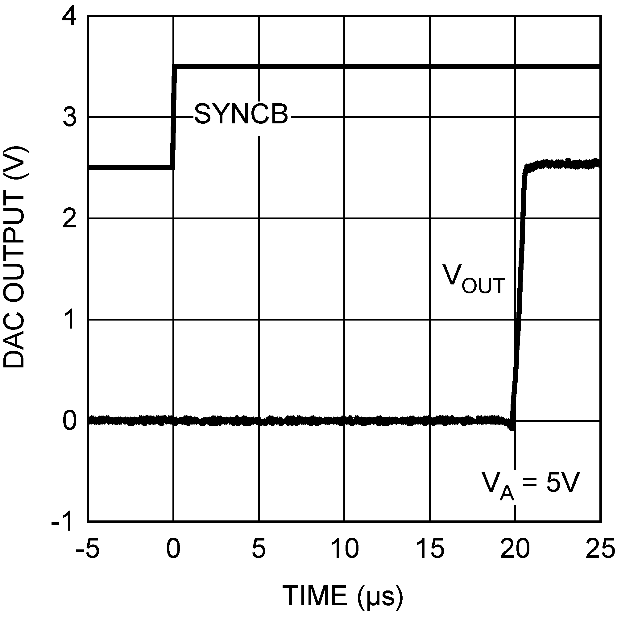
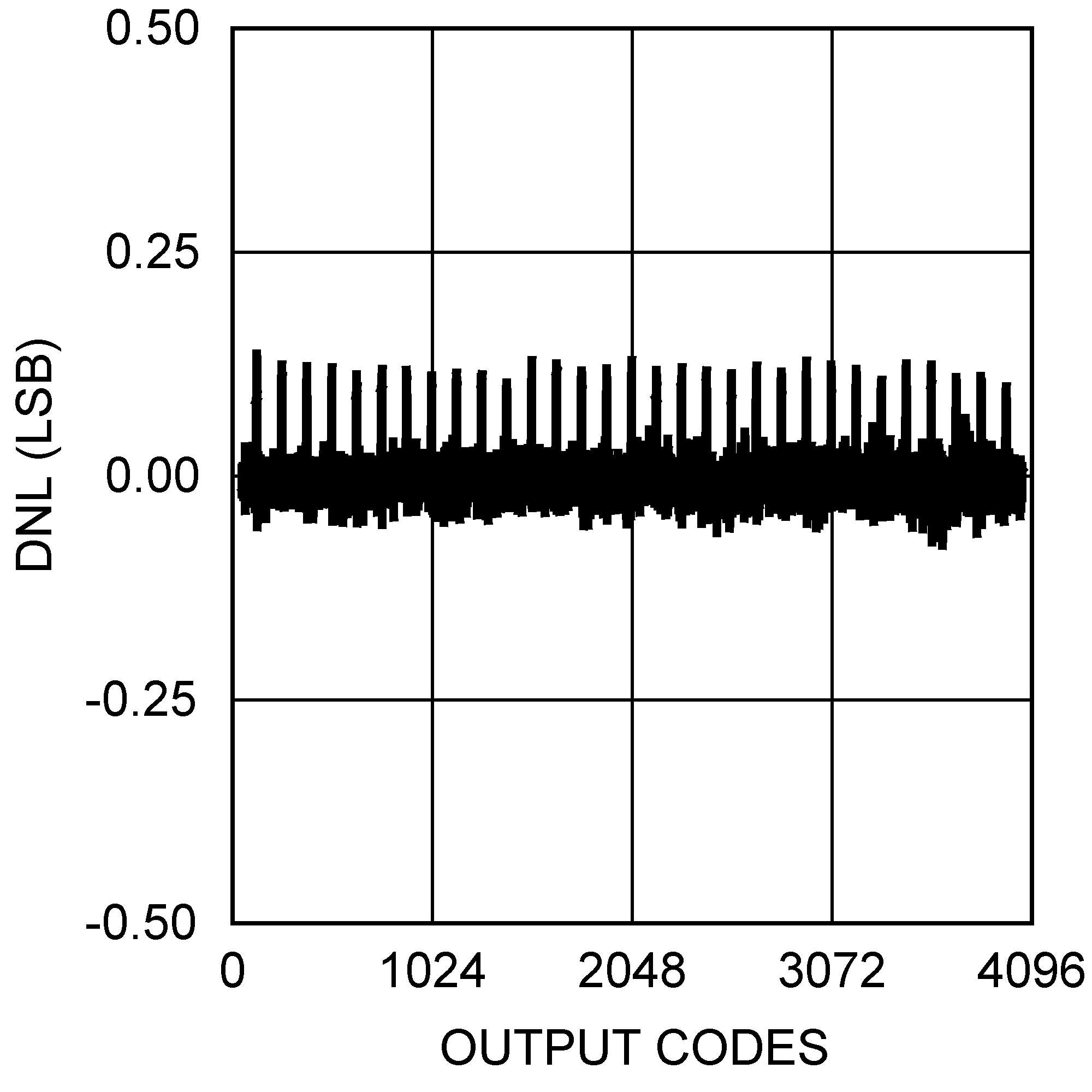
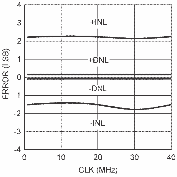
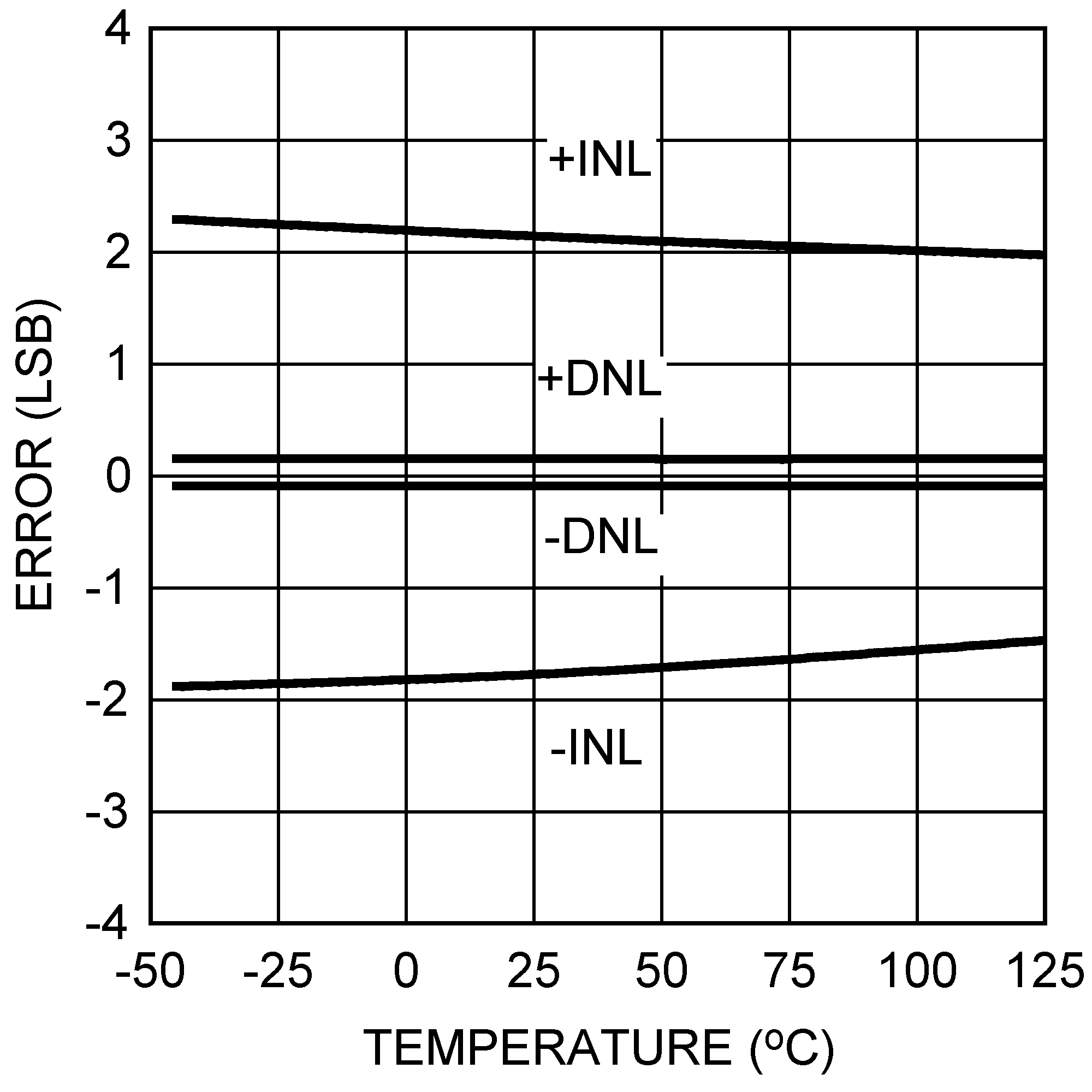
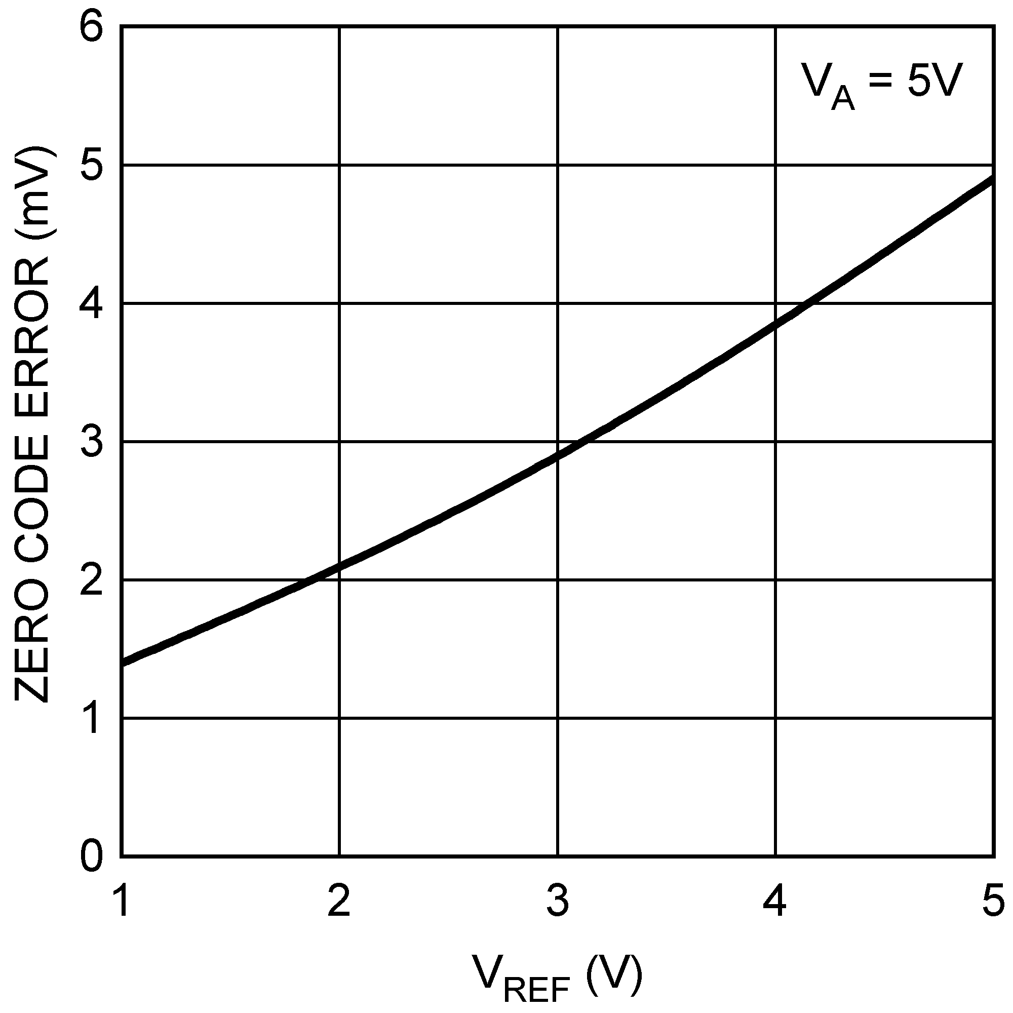
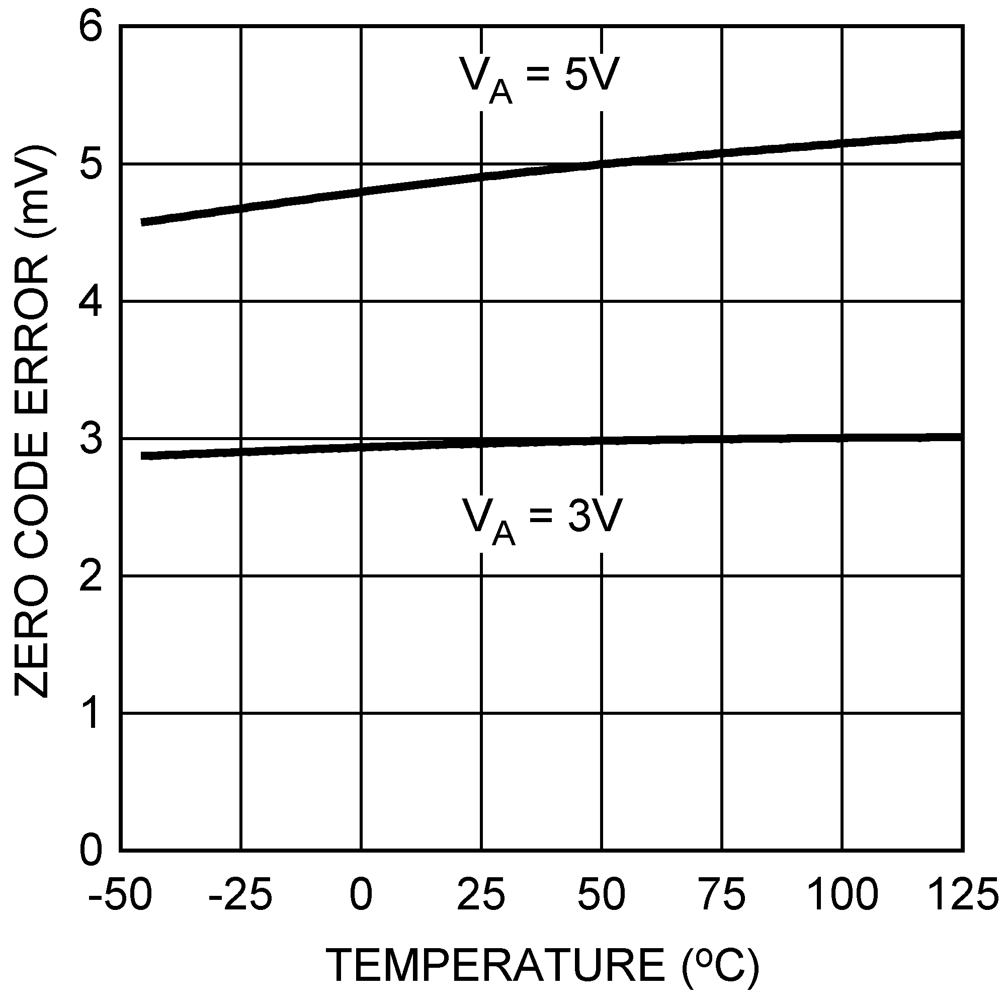
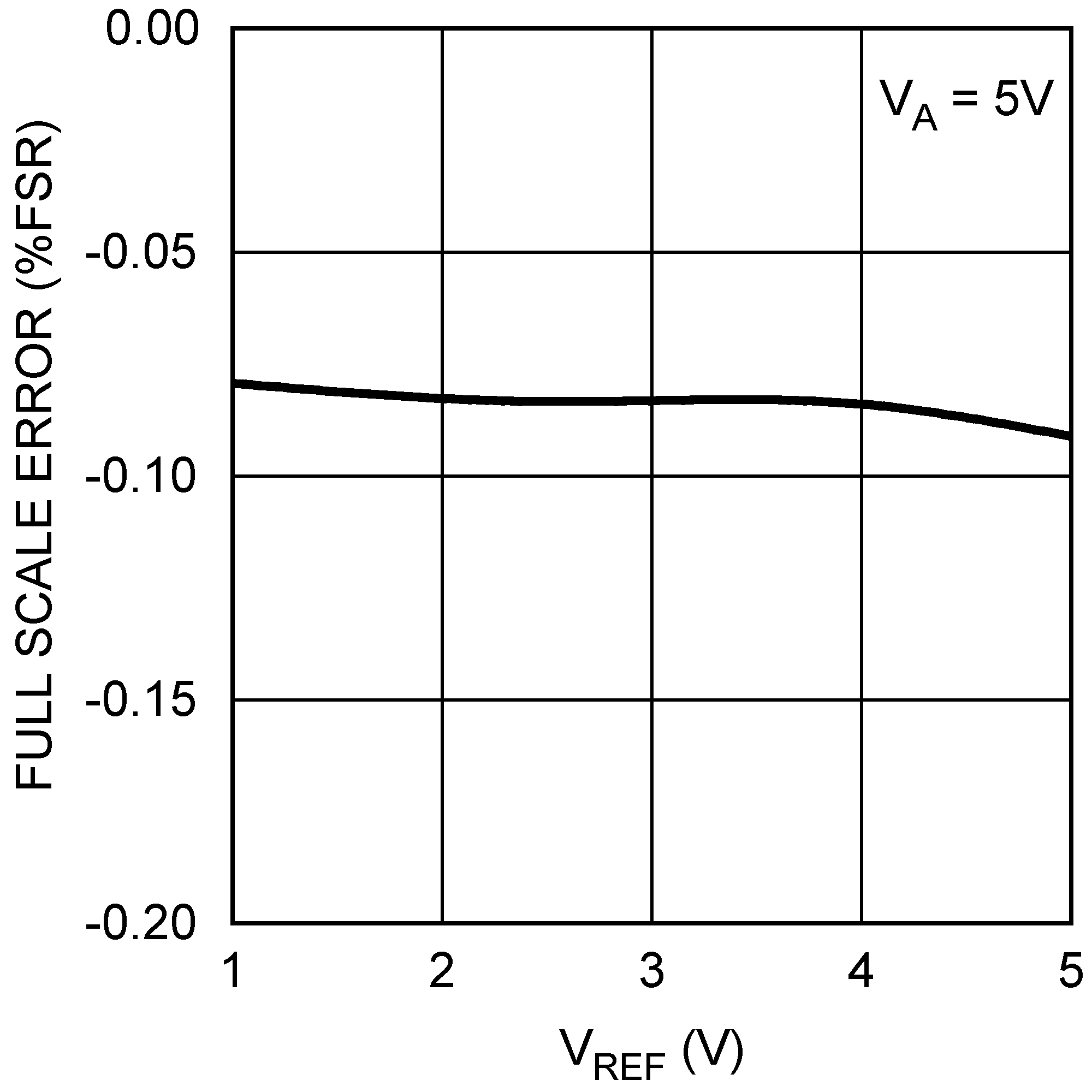
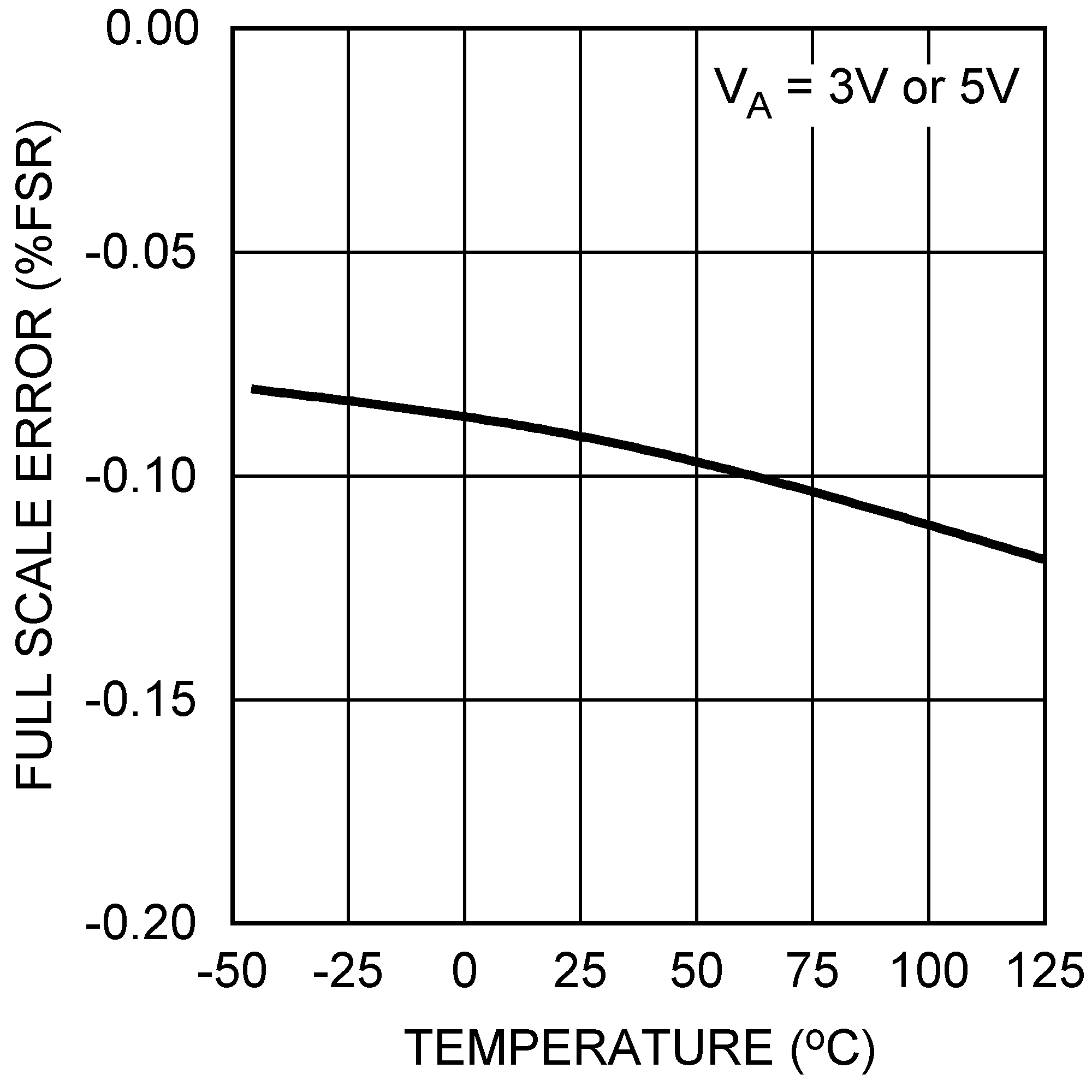
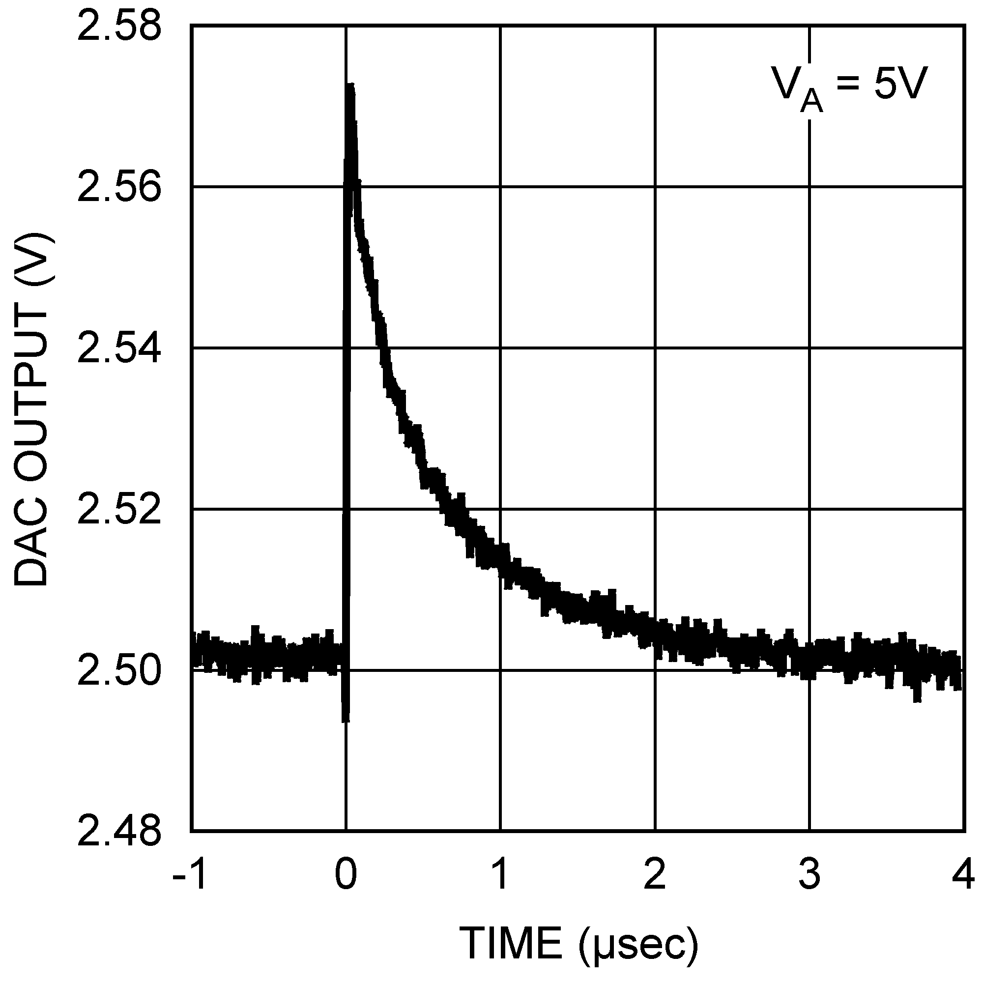
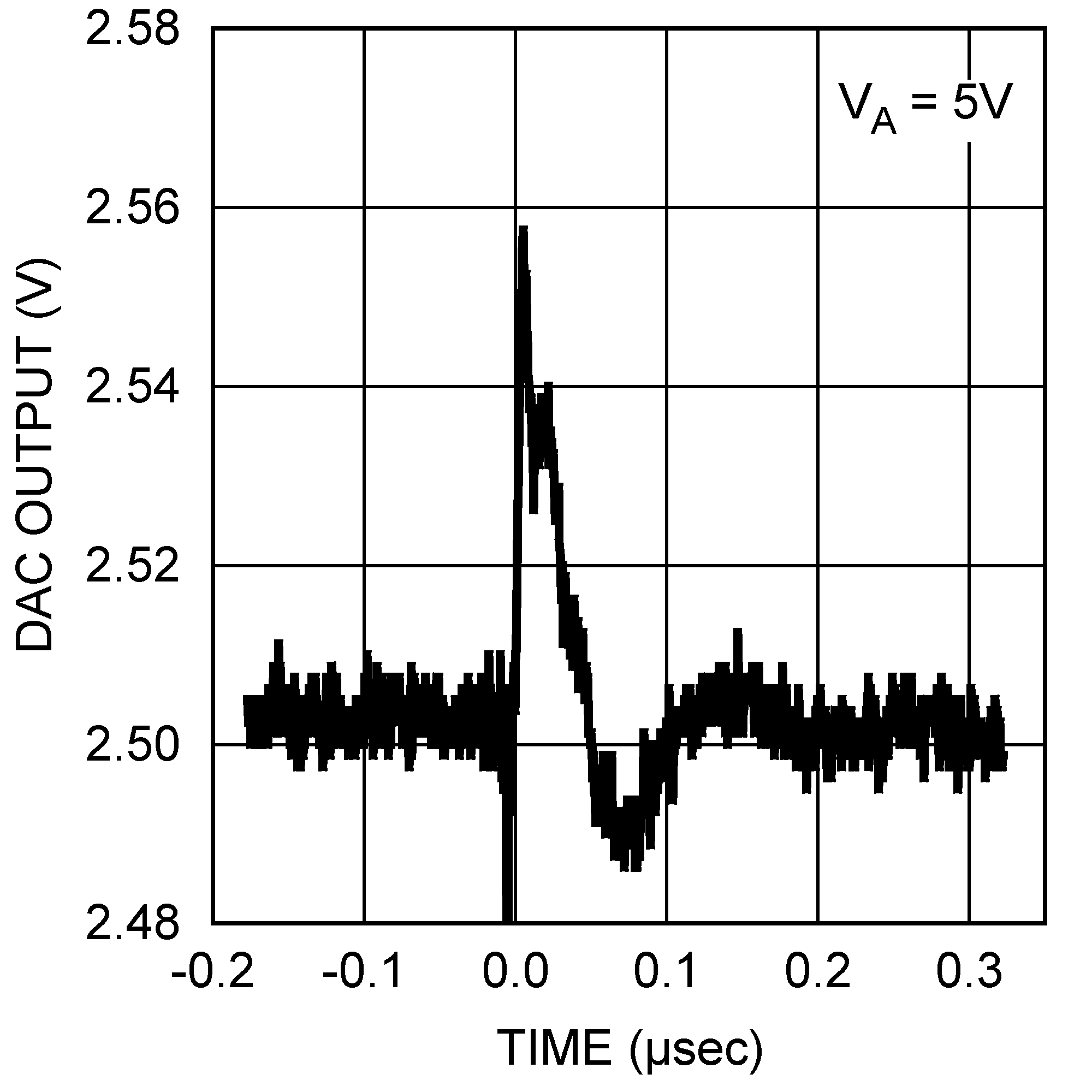
VA = 2.7 V to 5.5 V, VREF1,2 = VA, fSCLK = 30 MHz, TA = 25°C, unless otherwise stated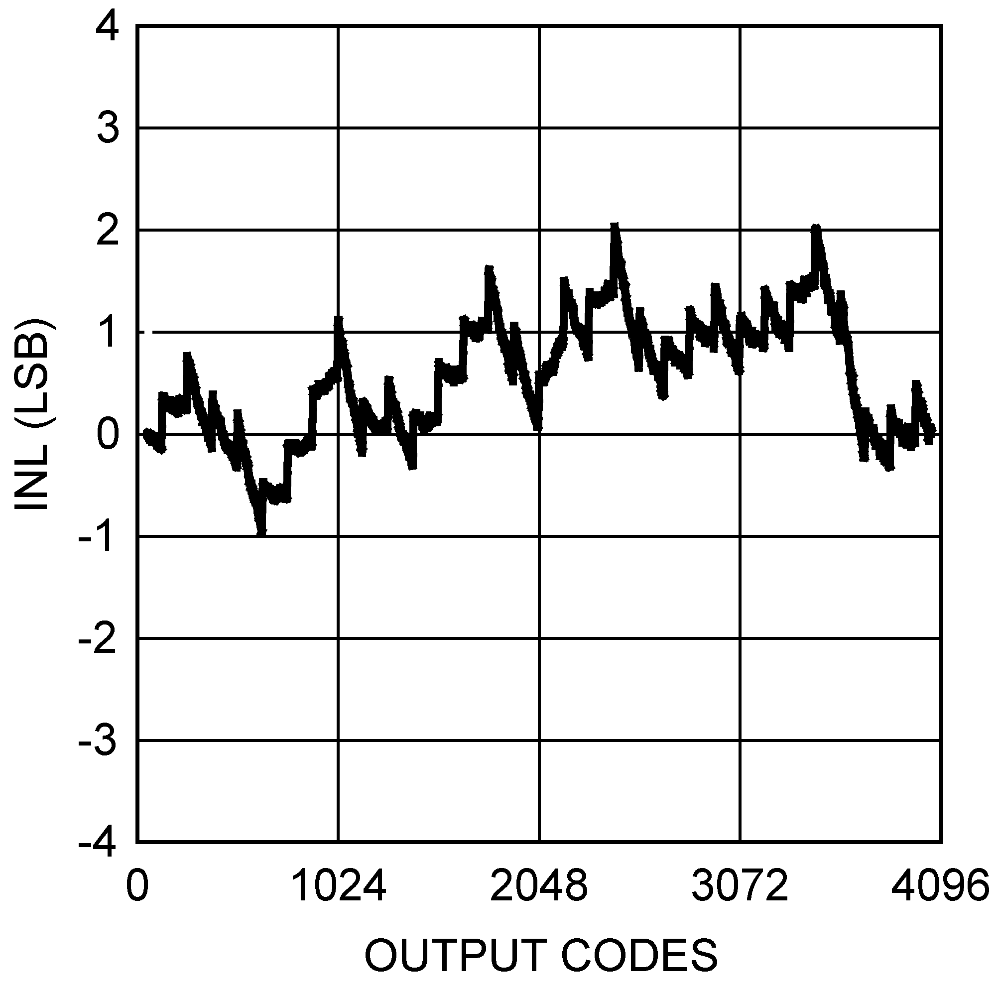
8 Detailed Description
8.1 Overview
The DAC128S085 is fabricated on a CMOS process with an architecture that consists of switches and resistor strings followed by an output buffer. The reference voltages are externally applied at VREF1 for DAC channels A through D, and VREF2 for DAC channels E through H.
8.2 Functional Block Diagram

8.3 Feature Description
8.3.1 DAC Architecture
For simplicity, a single resistor string is shown in Figure 26. This string consists of 4096 equal valued resistors with a switch at each junction of two resistors, plus a switch to ground. The code loaded into the DAC register determines which switch is closed, connecting the proper node to the amplifier. The input coding is straight binary with an ideal output voltage of:
where
- D is the decimal equivalent of the binary code that is loaded into the DAC register.
D can take on any value between 0 and 4095. This configuration ensures that the DAC is monotonic.
 Figure 26. DAC Resistor String
Because all eight DAC channels of the DAC128S085 can be controlled independently, each channel consists of a DAC register and a 12-bit DAC. Figure 27 is a simple block diagram of an individual channel in the DAC128S085. Depending on the mode of operation, data written into a DAC register causes the 12-bit DAC output to be updated, or an additional command is required to update the DAC output. Further description of the modes of operation can be found in Serial Interface.
 Figure 27. Single-Channel Block Diagram
8.3.2 Output Amplifiers
The output amplifiers are rail-to-rail, providing an output voltage range of 0 V to VA when the reference is VA. All amplifiers, including rail-to-rail types, exhibit a loss of linearity as the output approaches the supply rails (0 V and VA, in this case). For this reason, linearity is specified over less than the full output range of the DAC. However, if the reference is less than VA, only the lowest codes experience a loss in linearity.
The output amplifiers can drive a load of 2 kΩ in parallel with 1500 pF to ground or to VA. The zero-code and full-scale outputs for given load currents are available in the Electrical Characteristics.
8.3.3 Reference Voltage
The DAC128S085 uses dual external references, VREF1 and VREF2, which are shared by channels A, B, C, D and channels E, F, G, H, respectively. The reference pins are not buffered and have an input impedance of 30 kΩ. TI recommends driving VREF1 and VREF2 by voltage sources with low output impedance. The reference voltage range is 0.5 V to VA, providing the widest possible output dynamic range.
8.3.4 Serial Interface
The three-wire interface is compatible with SPI, QSPI, and MICROWIRE, as well as most DSPs, and operates at clock rates up to 40 MHz. A valid serial frame contains 16 falling edges of SCLK. See Table 1 for information on a write sequence.
A write sequence begins by bringing the SYNC line low. Once SYNC is low, the data on the DIN line is clocked into the 16-bit serial input register on the falling edges of SCLK. To avoid mis-clocking data into the shift register, it is critical that SYNC not be brought low on a falling edge of SCLK (see minimum and maximum setup times for SYNC in AC and Timing Characteristics and Figure 28). On the 16th falling edge of SCLK, the last data bit is clocked into the register. The write sequence is concluded by bringing the SYNC line high. Once SYNC is high, the programmed function (a change in the DAC channel address, mode of operation, or register contents) is executed. To avoid mis-clocking data into the shift register, it is critical that SYNC be brought high between the 16th and 17th falling edges of SCLK (see minimum and maximum hold times for SYNC in AC and Timing Characteristics and Figure 28).
 Figure 28. CS Setup and Hold Times
If SYNC is brought high before the 15th falling edge of SCLK, the write sequence is aborted and the data that has been shifted into the input register is discarded. If SYNC is held low beyond the 17th falling edge of SCLK, the serial data presented at DIN will begin to be output on DOUT. More information on this mode of operation can be found in Daisy-Chain Operation. In either case, SYNC must be brought high for the minimum specified time before the next write sequence is initiated with a falling edge of SYNC.
Since the DIN buffer draws more current when it is high, it should be idled low between write sequences to minimize power consumption. On the other hand, SYNC should be idled high to avoid the activation of daisy chain operation where DOUT is active.
8.3.5 Daisy-Chain Operation
Daisy-chain operation allows communication with any number of DAC128S085s using a single serial interface. As long as the correct number of data bits are input in a write sequence (multiple of sixteen bits), a rising edge of SYNC will properly update all DACs in the system.
To support multiple devices in a daisy chain configuration, SCLK and SYNC are shared across all DAC128S085s and DOUT of the first DAC in the chain is connected to DIN of the second. Figure 29 shows three DAC128S085s connected in daisy chain fashion. Similar to a single channel write sequence, the conversion for a daisy chain operation begins on a falling edge of SYNC and ends on a rising edge of SYNC. A valid write sequence for n devices in a chain requires n times 16 falling edges to shift the entire input data stream through the chain. Daisy chain operation is ensured for a maximum SCLK speed of 30 MHz.
 Figure 29. Daisy-Chain Configuration
The serial data output pin, DOUT, is available on the DAC128S085 to allow daisy-chaining of multiple DAC128S085 devices in a system. In a write sequence, DOUT remains low for the first 14 falling edges of SCLK before going high on the 15th falling edge. Subsequently, the next 16 falling edges of SCLK will output the first 16 data bits entered into DIN. Figure 30 shows the timing of 3 DAC128S085s in Figure 29. In this instance, It takes 48 falling edges of SCLK followed by a rising edge of SYNC to load all three DAC128S085s with the appropriate register data. On the rising edge of SYNC, the programmed function is executed in each DAC128S085 simultaneously.
When connecting multiple devices in a daisy-chain configuration, it is important to note that the DAC128S085 will update the DOUT signal on the falling edge of SCLK, and this will be sampled by the next DAC in the daisy chain on the next falling edge of the clock. Ensure that the timing requirements are met for proper operation. Specifically, pay attention to the data hold time after the SCLK falling (tDH) requirement. Improper layout or loading may delay the clock signal between devices. If delayed to the point that data changes prior to meeting the hold time requirement, incorrect data can be sampled. If the clock delay cannot be resolved, an alternative solution is to add a delay between the DOUT of one device and DIN of the following device in the daisy chain. This increases the hold time margin and allows for correct sampling. Be aware though, that the tradeoff with this fix is that too much delay eventually impacts the setup time.
 Figure 30. Daisy Chain Timing Diagram
8.3.6 DAC Input Data Update Mechanism
The DAC128S085 has two modes of operation, plus a few special command operations. The two modes of operation are Write Register Mode (WRM) and Write Through Mode (WTM). For the rest of this document, these modes will be referred to as WRM and WTM. The special command operations are separate from WRM and WTM because they can be called upon regardless of the current mode of operation. The mode of operation is controlled by the first four bits of the control register, DB15 through DB12. See Table 1 for a detailed summary.
Table 1. Write Register and Write Through Modes
| DB[15:12] | DB[11:0] | Description of Mode |
|---|---|---|
| 1 0 0 0 | X X X X X X X X X X X X | WRM: The registers of each DAC Channel can be written to without causing their outputs to change. |
| 1 0 0 1 | X X X X X X X X X X X X | WTM: Writing data to a channel's register causes the DAC output to change. |
When the DAC128S085 first powers up, the DAC is in WRM. In WRM, the registers of each individual DAC channel can be written to without updating the DAC outputs. This is accomplished by setting DB15 to 0, specifying the DAC register to be written to in DB[14:12], and entering the new DAC register setting in DB[11:0] (see Table 2). The DAC128S085 remains in WRM until the mode of operation is changed to WTM. The mode of operation is changed from WRM to WTM by setting DB[15:12] to 1001. Once in WTM, writing data to a DAC channel register causes the DAC output to be updated as well. Changing a DAC channel register in WTM is accomplished in the same manner as in WRM. However, in WTM the DAC register and output are updated at the completion of the command (see Table 2). Similarly, the DAC128S085 remains in WTM until the mode of operation is changed to WRM by setting DB[15:12] to 1000.
Table 2. Commands Impacted by WRM and WTM
| DB15 | DB[14:12] | DB[11:0] | Description of Mode |
|---|---|---|---|
| 0 | 0 0 0 | D11 D10 ... D1 D0 | WRM: D[11:0] written to ChA's data register only WTM: ChA's output is updated by data in D[11:0] |
| 0 | 0 0 1 | D11 D10 ... D1 D0 | WRM: D[11:0] written to only the data register of ChB WTM: ChB's output is updated by data in D[11:0] |
| 0 | 0 1 0 | D11 D10 ... D1 D0 | WRM: D[11:0] written to only the data register of ChC WTM: ChC's output is updated by data in D[11:0] |
| 0 | 0 1 1 | D11 D10 ... D1 D0 | WRM: D[11:0] written only the data register of ChD WTM: ChD's output is updated by data in D[11:0] |
| 0 | 1 0 0 | D11 D10 ... D1 D0 | WRM: D[11:0] written only the data register of ChE WTM: ChE's output is updated by data in D[11:0] |
| 0 | 1 0 1 | D11 D10 ... D1 D0 | WRM: D[11:0] written only the data register of ChF WTM: ChF's output is updated by data in D[11:0] |
| 0 | 1 1 0 | D11 D10 ... D1 D0 | WRM: D[11:0] written only the data register of ChG WTM: ChG's output is updated by data in D[11:0] |
| 0 | 1 1 1 | D11 D10 ... D1 D0 | WRM: D[11:0] written only the data register of ChH WTM: ChH's output is updated by data in D[11:0] |
The special command operations can be exercised at any time regardless of the mode of operation. There are three special command operations. The first command is exercised by setting data bits DB[15:12] to 1010. This allows the user to update multiple DAC outputs simultaneously to the values currently loaded in their respective control registers. This command is valuable if the user wants each DAC output to be at a different output voltage, but still have all the DAC outputs changed to their appropriate values simultaneously (see Table 3).
The second special command allows the user to alter the DAC output of channel A with a single write frame. This command is exercised by setting data bits DB[15:12] to 1011 and data bits DB[11:0] to the desired control register value. This command also causes the DAC outputs of the other channels to update to their current control register values. The user may choose to exercise this command to save a write sequence. For example, the user may wish to update several DAC outputs simultaneously, including channel A. To accomplish this task in the minimum number of write frames, the user would alter the control register values of all the DAC channels except channel A while operating in WRM. The last write frame would be used to exercise the special command Channel A Write Mode. In addition to updating the control register of channel A and output to a new value, all of the other channels would be updated as well. At the end of this sequence of write frames, the DAC128S085 would still be operating in WRM (see Table 3).
The third special command allows the user to set all the DAC control registers and outputs to the same level. This command is commonly referred to as "broadcast" mode, as the same data bits are being broadcast to all of the channels simultaneously. This command is exercised by setting data bits DB[15:12] to 1100 and data bits DB[11:0] to the value that the user wishes to broadcast to all the DAC control registers. Once the command is exercised, each DAC output is updated by the new control register value. This command is frequently used to set all the DAC outputs to some known voltage such as 0 V, VREF/2, or Full Scale. A summary of the commands can be found in Table 3.
Table 3. Special Command Operations
| DB[15:12] | DB[11:0] | Description of Mode |
|---|---|---|
| 1 0 1 0 | X X X X H G F E D C B A | Update Select: The DAC outputs of the channels selected with a 1 in DB[7:0] are updated simultaneously to the values in their respective control registers. |
| 1 0 1 1 | D11 D10 ... D1 D0 | Channel A Write: The control register and DAC output of channel A are updated to the data in DB[11:0]. The outputs of the other seven channels are also updated according to their respective control register values. |
| 1 1 0 0 | D11 D10 ... D1 D0 | Broadcast: The data in DB[11:0] is written to all channel control registers and DAC output simultaneously. |
8.3.7 Power-On Reset
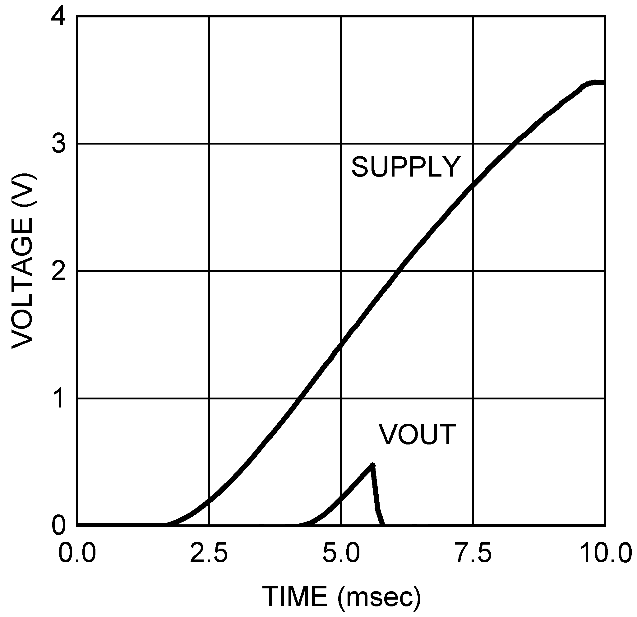
The power-on reset circuit controls the output voltages of the eight DACs during power-up. Upon application of power, the DAC registers are filled with zeros and the output voltages are set to 0 V. The outputs remain at 0 V until a valid write sequence is made.
8.3.8 Transfer Characteristic
 Figure 31. Input / Output Transfer Characteristic
8.4 Device Functional Modes
8.4.1 Power-Down Modes
The DAC128S085 has three power-down modes, where different output terminations can be selected (see Table 4). With all channels powered down, the supply current drops to 0.1 µA at 3 V and 0.2 µA at 5 V. By selecting the channels to be powered down in DB[7:0] with a 1, individual channels can be powered down separately, or multiple channels can be powered down simultaneously. The three different output terminations include high output impedance, 100 kΩ to ground, and 2.5 kΩ to ground.
The output amplifiers, resistor strings, and other linear circuitry are all shut down in any of the power-down modes. The bias generator, however, is only shut down if all the channels are placed in power-down mode. The contents of the DAC registers are unaffected when in power-down. Therefore, each DAC register maintains its value prior to the DAC128S085 being powered down unless it is changed during the write sequence that instructed it to recover from power down. Minimum power consumption is achieved in the power-down mode with SYNC idled high, DIN idled low, and SCLK disabled. The time to exit power-down (Wake-Up Time) is typically 3 µsec at 3 V and 20 µsec at 5 V.
Table 4. Power-Down Modes
| DB[15:12] | DB[11:8] | 7 | 6 | 5 | 4 | 3 | 2 | 1 | 0 | Output Impedance |
|---|---|---|---|---|---|---|---|---|---|---|
| 1 1 0 1 | X X X X | H | G | F | E | D | C | B | A | Hi-Z outputs |
| 1 1 1 0 | X X X X | H | G | F | E | D | C | B | A | 100 kΩ outputs |
| 1 1 1 1 | X X X X | H | G | F | E | D | C | B | A | 2.5 kΩ outputs |
8.5 Programming
8.5.1 Programming the DAC128S085
This section presents the step-by-step instructions for programming the serial input register.
8.5.1.1 Updating DAC Outputs Simultaneously
When the DAC128S085 is first powered on, the DAC is operating in Write Register Mode (WRM). Operating in WRM allows the user to program the registers of multiple DAC channels without causing the DAC outputs to be updated. For example, below are the steps for setting Channel A to a full scale output, Channel B to three-quarters full scale, Channel C to half-scale, Channel D to one-quarter full scale and having all the DAC outputs update simultaneously.
As stated previously, the DAC128S085 powers up in WRM. If the device was previously operating in Write Through Mode (WTM), an extra step to set the DAC into WRM is required. First, the DAC registers must be programmed to the desired values. To set Channel A to an output of full scale, write 0FFF to the control register. This updates the data register for Channel A without updating the output of Channel A. Second, set Channel B to an output of three-quarters full scale by writing 1C00 to the control register. This updates the data register for Channel B. Once again, the output of Channel B and Channel A are not updated, because the DAC is operating in WRM. Third, set Channel C to half scale by writing 2800 to the control register. Fourth, set Channel D to one-quarter full scale by writing 3400 to the control register. Finally, update all four DAC channels simultaneously by writing A00F to the control register. This procedure allows the user to update four channels simultaneously with five steps.
Because Channel A was one of the DACs to be updated, one command step could have been saved by writing to Channel A last. Do this by writing to Channel B, C, and D first, and using the the special command Channel A Write to update the DAC register and output of Channel A. This special command also updates all DAC outputs while updating Channel A. With this sequence of commands, the user can update four channels simultaneously using four steps. A summary of this command can be found in Table 3.
8.5.1.2 Updating DAC Outputs Independently
If the DAC128S085 is currently operating in WRM, change the mode of operation to WTM by writing 9XXX to the control register. Once the DAC is operating in WTM, any DAC channel can be updated in one step. For example, if a design required Channel G to be set to half scale, the user can write 6800 to the control register to update the data register and DAC output of Channel G. Similarly, write 5FFF to the control register to set the output of Channel F to full scale. Channel A is the only channel that has a special command that allows its DAC output to be updated in one command, regardless of the mode of operation. Write BFFF to the control register to set the DAC output of Channel A to full scale in one step.
9 Application and Implementation
NOTE
Information in the following applications sections is not part of the TI component specification, and TI does not warrant its accuracy or completeness. TI’s customers are responsible for determining suitability of components for their purposes. Customers should validate and test their design implementation to confirm system functionality.
9.1 Application Information
9.1.1 Using References as Power Supplies
While the simplicity of the DAC128S085 implies ease of use, it is important to recognize that the path from the reference input (VREF1,2) to the DAC outputs has a zero Power Supply Rejection Ratio (PSRR). Therefore, the user must provide a noise-free supply voltage to VREF1,2. To utilize the full dynamic range of the DAC128S085, the supply pin (VA) and VREF1,2 can be connected together and share the same supply voltage. Because the DAC128S085 consumes very little power, a reference source can be used as the reference input or the supply voltage. The advantages of using a reference source over a voltage regulator are accuracy and stability. Some low-noise regulators can also be used. Listed below are a few reference and power supply options for the DAC128S085.
9.2 Typical Application
The LM4132, with its ±0.05% accuracy over temperature, is a good choice as a reference source for the DAC128S085. The 4.096-V version is useful for a 0-V to 4.095-V output range. Bypassing the LM4132 voltage input pin with a 4.7-µF capacitor and the voltage output pin with a 4.7-µF capacitor improves stability and reduces output noise. The LM4132 comes in a space-saving 5-pin SOT-23.
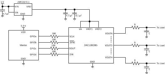 Figure 32. The LM4132 as a Power Supply
9.2.1 Design Requirements
There are two references for the DAC128S085. One reference input serves channels A through D, while the other reference serves channels E through H. The 16-bit input shift register of the DAC128S085 controls the mode of operation, the power-down condition, and the register/output value of the DAC channels. All eight DAC outputs can be updated simultaneously or individually.
9.2.2 Detailed Design Procedure
Each reference input pin can be set independently, or the reference pins can be shorted together as shown in Figure 32. Acceptable reference voltages are 0.5 V to VA. Utilizing an RC filter on the output to roll off output noise is optional.
9.2.3 Application Curve
 Figure 33. Typical Performance