SNAA364 June 2022 ADC128S102-SEP
1 Application Brief
Introduction to Satellite Telemetry
The popularity of low Earth orbit (LEO) mission profiles in satellite applications continues to grow for commercial, scientific, and even military applications. These missions are typically deployed in a satellite constellation, or group of satellites working together as a unified system. In contrast, historical single-satellite deployments which are meant to stay in geosynchronous orbit (GEO) for long periods of time with strict reliability concerns.
 Figure 1-1 Graphic Illustration of Satellite Constellation
This shift creates an opportunity for lighter, smaller, lower cost plastic package offerings versus conventional ceramic packaging traditionally used in space applications. These packages are usually large, expensive, and heavy when compared to their terrestrial counterparts in conventional plastic packages, although they are still required to fulfill their purpose in GEO applications.
Virtually every satellite, whether GEO or LEO, is launched with a variety of internal diagnostic measurements used to monitor start-up and run-time health of the satellite as well as detecting various fault conditions. Almost every module within the satellite will have monitoring functionality, typically realized in the form of voltage and current measurement circuits for each power-supply rail and coarse module temperature measurements. The number of diagnostic channels in an entire satellite can quickly reach > 100 channels as the number of modules within a satellite grow, making it all the more important to have low-cost, small, and lightweight voltage, current, and temperature-sensing solutions.
Analog-to-Digital Converters for Satellite Telemetry
An analog-to-digital converter (ADC) is the center of these telemetry measurements and the ADC128S102QML-SP device has a longer flight heritage than any other general-purpose ADC, with more than 15 years of flight missions.
The ADC128S102 core is a 12-bit, 1-MSPS, 8-channel, unbuffered SAR ADC with a serial peripheral interface (SPI), which when operated at lower data-rates does not require an external buffer. This feature makes it an ideal and simple candidate for diagnostic functionality.
Texas Instruments released a Space Enhanced Plastic (SEP) edition of the ADC128S102 core, named ADC128S102-SEP targeting LEO applications to complement the existing ADC128S102QML-SP for GEO applications. The two devices deliver the same analog parametric performance and same functional feature-set.
While the use of a plastic package aids in the reduction of cost, size, and weight, it comes with a radiation-hardened performance trade-off versus what can be offered in ceramic packaging. Table 1-1 summarizes the comparison of total ionizing dose (TID) and single-event latch-up (SEL) performance.
| Device | TID Rating | SEL Rating |
|---|---|---|
100 krad (Si) | 120 MeV-cm2/mg | |
30 krad (Si) | 43 MeV-cm2/mg |
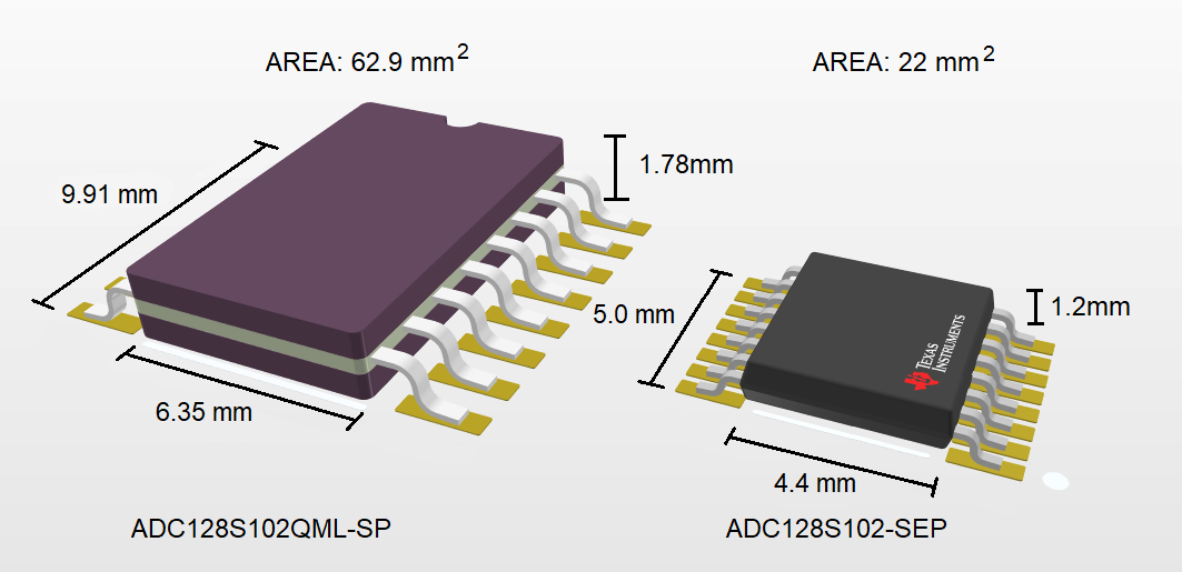
The ADC128S102-SEP comes in a 16-pin thin-shrink small-outline package (TSSOP) which is roughly 60% smaller than the hermetically sealed 16-pin ceramic flat pack (CFP) package for the ADC128S102QML-SP.
Figure 1-2 contrasts the size differences between the ceramic and plastic packaging.
 Figure 1-2 ADC128S102QML-SP and ADC128S102-SEP Package Size Comparison
The following sections briefly discuss common circuits implemented with the ADC128S102-SEP for voltage, current, and temperature sensing.
Voltage Sensing With ADC128S102-SEP
Voltage sensing solutions aboard LEO satellites are most commonly implemented in power-supply module diagnostics along with various other telemetry applications, motor drives, battery cell balancing and charging, electric cooler control, and RF amplifier biasing.
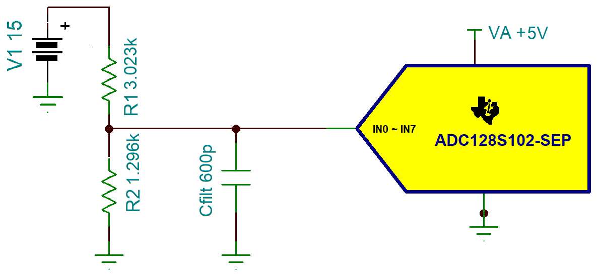
In most instances these applications require measuring voltages outside of the input range of a typical precision ADC, which often do not exceed 5 V. A simple voltage divider can be implemented to accurately use the full scale range of the ADC, as shown with the example 15-V input in Figure 1-3.
 Figure 1-3 50-kSPS Voltage Sensing Circuit With ADC128S102-SEP
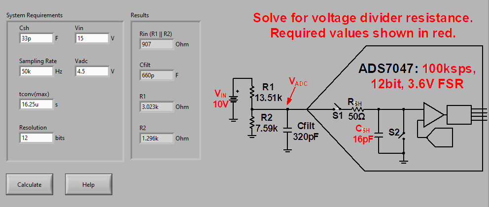
In this example the ADC sample rate is assumed to be relatively low, 50 kSPS, versus the 1 MSPS maximum sample rate. This data-rate in tandem with the input capacitor Cfilt remove dependency on an external buffer to drive a settled voltage, within ½ a least significant bit (LSB), at the input of SAR converter. The ADC Drive Without Amplifier section of the Analog Engineer’s Calculator can be used to size the value of R1, R2, and Cfilt after seeding the tool with the input voltage range, resolution, sampling rate, and conversion time of the ADC as well as the value of the DC voltage to be sensed. This example is shown in Figure 1-4.
 Figure 1-4 Passive Component Values Calculated From the Analog Engineer's Calculator
This circuit is verified to settle within ½ LSB in SPICE and the previously-mentioned tools can also be leveraged to configure alternative data-rates. It is key to choose low data-rates to remove the need for an external buffer and save size.
Current Sensing With ADC128S102-SEP
Current sensing circuits are most often used along-side their voltage sensing counter-parts for monitoring power-supply integrity, most notably monitoring for undercurrent or overcurrent conditions which may suggest integrated circuit latch-up or other hazardous conditions concerning operation of the satellite. Current sensing may also find use cases in motor drives, solar cell current sensing, battery cell charging applications.
There are a variety of potential solutions for current sensing with the ADC128S102-SEP, but this example focuses on a similarly small footprint solution at the same, or similar, data-rate as the voltage sensing application for a straightforward design. Figure 1-5 shows the example circuit, operating at 50 kSPS minimum, and including an external shunt resistor and input filter along with the INA240-SEP, a SEP rated instrumentation amplifier.
 Figure 1-5 195-kSPS Current Sensing Circuit With ADC128S102-SEP
REF1 and REF2 of the INA240-SEP are connected to GND to facilitate a GND referenced output signal, or 0-V output for 0-A input current. The INA240-SEP gain is fixed to 20 V/V, so the shunt resistor is sized to deliver a full-scale output voltage of 4.5 V for a full-scale input current of 20 A.
Input capacitor C2 is sized to be approximately 20 times the value of the internal sampling capacitor of the ADC128S102-SEP and R1 is optimized using SPICE for the maximum sampling rate of 195 kSPS.
Circuit modifications may be implemented to increase the bandwidth of the current measurement in fault-critical applications which may need to be acknowledged quickly.
Temperature Sensing With ADC128S102-SEP
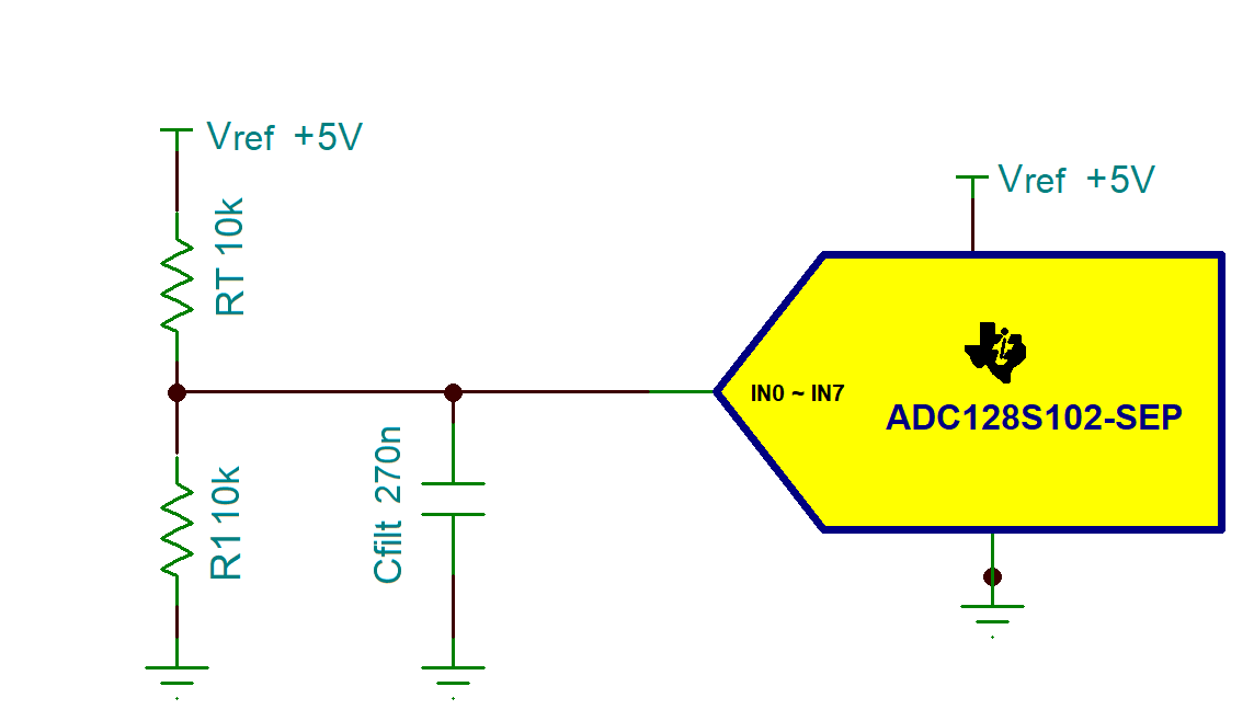
 Figure 1-6 Temperature Sensing Circuit With ADC128S102-SEP
This temperature sensing circuit is similarly designed to the voltage sensing circuit ; however, the upper divider resistor is replaced by an NTC or PTC thermistor. TI recommends calculating the R1 and Cfilt values using the Analog Engineer's Calculator - ADC Drive Without Amplifier periodic single shot mode to ensure a 1 LSB or less signal settling error.
Conclusion
The increasing requirements for LEO flight profiles in commercial, scientific, and military applications requires new ADC offerings for current, voltage, temperature, and other telemetry measurements. The plastic package ADC128S102-SEP is a great complement to the ceramic packaged ADC128S102QML-SP and builds out TI's portfolio of ADCs for LEO and GEO applications.