-
TPS61071-Q1 90% Efficient Synchronous Boost Converter With 600-mA Switch
- 1 Features
- 2 Applications
- 3 Description
- 4 Revision History
- 5 Pin Configuration and Functions
- 6 Specifications
- 7 Detailed Description
- 8 Application and Implementation
- 9 Power Supply Recommendations
- 10Layout
- 11Device and Documentation Support
- 12Mechanical, Packaging, and Orderable Information
- IMPORTANT NOTICE
TPS61071-Q1 90% Efficient Synchronous Boost Converter With 600-mA Switch
1 Features
- Qualified for Automotive Applications
- AEC-Q100 Qualified With the Following Results:
- Device Temperature Grade 2: –40°C to 105°C Ambient Operating Temperature Range
- Device HBM Classification Level 1C
- Device CDM Classification Level C6
- 90% Efficient Synchronous Boost Converter
- 75-mA Output Current at 3.3 V From 0.9-V Input
- 150-mA Output Current at 3.3 V From 1.8-V Input
- Device Quiescent Current: 19 µA (Typical)
- Input Voltage Range: 0.9 V to 5.5 V
- Adjustable Output Voltage Up to 5.5 V
- Power-Save Mode Version Available for
Improved Efficiency at Low Output Power - Load Disconnect During Shutdown
- Overtemperature Protection
- Small 6-Pin Thin SOT Package
2 Applications
- Automotive Power Supplies
- Boost Power Supplies
3 Description
The TPS61071-Q1 device provides a power supply solution for products powered by lower-voltage DC rails or a one-cell, two-cell, or three-cell alkaline, NiCd or NiMH, or one-cell Li-ion or Li-polymer battery. Output currents can go as high as 75 mA, while using a single-cell alkaline, and discharge down to 0.9 V. The device can also generate 5 V at 200 mA from a 3.3-V rail or a Li-ion battery. The boost converter is based on a fixed frequency, pulse-width-modulation (PWM) controller using a synchronous rectifier to obtain maximum efficiency. The maximum peak current in the boost switch is limited typically to a value of 600 mA.
The TPS61071-Q1 output voltage is programmed by an external resistor divider. To minimize battery drain, disable the converter. During shutdown, the load disconnects from the battery. The device package is a 6-pin thin SOT package (DDC).
Device Information(1)
| PART NUMBER | PACKAGE | BODY SIZE (NOM) |
|---|---|---|
| TPS61071-Q1 | SOT (6) | 1.60 mm × 2.90 mm |
- For all available packages, see the orderable addendum at the end of the data sheet.
Typical Application Circuit

4 Revision History
Changes from * Revision (May 2010) to A Revision
- Added ESD Ratings table, Feature Description section, Device Functional Modes, Application and Implementation section, Power Supply Recommendations section, Layout section, Device and Documentation Supportsection, and Mechanical, Packaging, and Orderable Information sectionGo
- Changed pinout illustration.Go
- Deleted Dissipation Ratings sectionGo
- Updated Soft Start and Short-Circuit Protection sectionGo
- Updated Device EnablesectionGo
- Changed Figure 20Go
- Updated Inductor Selection sectionGo
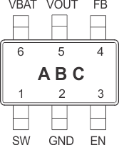
5 Pin Configuration and Functions
Pin Functions
| PIN | I/O | DESCRIPTION | |
|---|---|---|---|
| NO. | NAME | ||
| 1 | SW | I | Boost and rectifying switch input |
| 2 | GND | — | Device (IC) ground connection for logic and power |
| 3 | EN | I | Enable input (1/VBAT enabled, 0/GND disabled) |
| 4 | FB | I | Voltage feedback for programming the output voltage |
| 5 | VOUT | O | Boost converter output |
| 6 | VBAT | I | Supply voltage |
6 Specifications
6.1 Absolute Maximum Ratings
over operating free-air temperature range (unless otherwise noted)(1)| MIN | MAX | UNIT | |
|---|---|---|---|
| Input voltage range on SW, VOUT, VBAT, EN, FB | –0.3 | 7 | V |
| Operating virtual junction temperature, TJ | –40 | 150 | °C |
| Storage temperature, Tstg | –65 | 150 | °C |
6.2 ESD Ratings
| VALUE | UNIT | |||
|---|---|---|---|---|
| V(ESD) | Electrostatic discharge | Human-body model (HBM), per AEC Q100-002(1) | ±2000 | V |
| Charged-device model (CDM), per AEC Q100-011 | ±1000 | |||
6.3 Recommended Operating Conditions
| MIN | NOM | MAX | UNIT | |
|---|---|---|---|---|
| Supply voltage at VBAT, VI | 0.9 | 5.5 | V | |
| Operating free air temperature range, TA | –40 | 105 | °C | |
| Operating virtual junction temperature range, TJ | –40 | 125 | °C |
6.4 Thermal Information
| THERMAL METRIC(1) | TPS61071-Q1 | UNIT | |
|---|---|---|---|
| DDC (SOT) | |||
| 6 PINS | |||
| RθJA | Junction-to-ambient thermal resistance | 139.1 | °C/W |
| RθJC(top) | Junction-to-case (top) thermal resistance | 34.8 | °C/W |
| RθJB | Junction-to-board thermal resistance | 42.5 | °C/W |
| ψJT | Junction-to-top characterization parameter | 1.4 | °C/W |
| ψJB | Junction-to-board characterization parameter | 40.7 | °C/W |
| RθJC(bot) | Junction-to-case (bottom) thermal resistance | N/A | °C/W |
6.5 Electrical Characteristics
over recommended free-air temperature range and over recommended input voltage range (typical at an ambient temperature range of 25°C) (unless otherwise noted)| PARAMETER | TEST CONDITIONS | MIN | TYP | MAX | UNIT | ||
|---|---|---|---|---|---|---|---|
| DC-DC STAGE | |||||||
| VI | Minimum input voltage range for start-up | RL = 270 Ω | 1.1 | 1.25 | V | ||
| Input voltage range, after start-up | TA = 25°C | 0.9 | 5.5 | ||||
| VO | Output voltage range | 1.8 | 5.5 | V | |||
| V(FB) | Feedback voltage | TA = 25°C | 490 | 500 | 510 | mV | |
| f | Oscillator frequency | 960 | 1200 | 1440 | kHz | ||
| I(SW) | Switch current limit | VOUT= 3.3 V | 455 | 600 | 735 | mA | |
| Start-up current limit | 0.5 × ISW | mA | |||||
| Boost switch-on resistance | VOUT= 3.3 V | 480 | mΩ | ||||
| Rectifying switch-on resistance | VOUT= 3.3 V | 600 | mΩ | ||||
| Total accuracy (including line and load regulation) | 5% | ||||||
| Line regulation | 1% | ||||||
| Load regulation | 1% | ||||||
| Quiescent current | VBAT | IO= 0 mA, V(EN)= VBAT = 1.2 V, VOUT = 3.3 V, TA = 25°C |
0.5 | 1 | µA | ||
| VOUT | 190(1) | 300(1) | |||||
| 20(2) | |||||||
| Shutdown current | V(EN) = 0 V, VBAT = 1.2 V, TA = 25°C | 0.05 | 0.5 | µA | |||
| CONTROL STAGE | |||||||
| V(UVLO) | Undervoltage lockout threshold | V(BAT) voltage decreasing | 0.8 | V | |||
| VIL | EN input low voltage | 0.2 × VBAT | V | ||||
| VIH | EN input high voltage | 0.8 × VBAT | V | ||||
| EN input current | Clamped on GND or VBAT | 0.01 | 0.1 | µA | |||
| Overtemperature protection | 140 | °C | |||||
| Overtemperature hysteresis | 20 | °C | |||||
6.6 Typical Characteristics
Table 1. Table of Graphs
| FIGURE | ||
|---|---|---|
| Maximum output current | vs Input voltage | Figure 1 |
| Efficiency | vs Output current | Figure 2 |
| vs Output current | Figure 3 | |
| vs Output current | Figure 4 | |
| vs Input voltage | Figure 5 | |
| vs Input voltage | Figure 6 | |
| Output voltage | vs Output current | Figure 7 |
| vs Output current | Figure 8 | |
| No load supply current into VOUT | vs Input voltage | Figure 9 |
| Waveforms | Output voltage in continuous mode | Figure 10 |
| Output voltage in continuous mode | Figure 11 | |
| Load transient response | Figure 12 | |
| Load transient response | Figure 13 | |
| Line transient response | Figure 14 | |
| Line transient response | Figure 15 | |
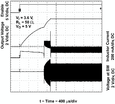
| Start-up after enable | Figure 16 | |
| Start-up after enable | Figure 17 |
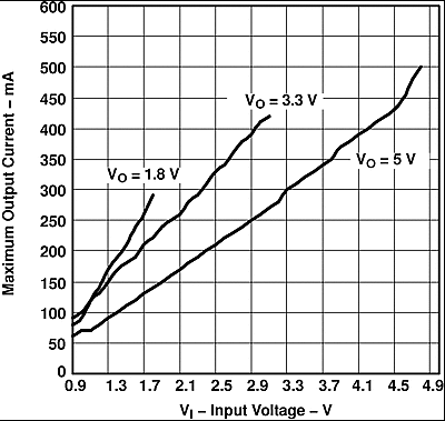 Figure 1. Maximum Output Current vs Input Voltage
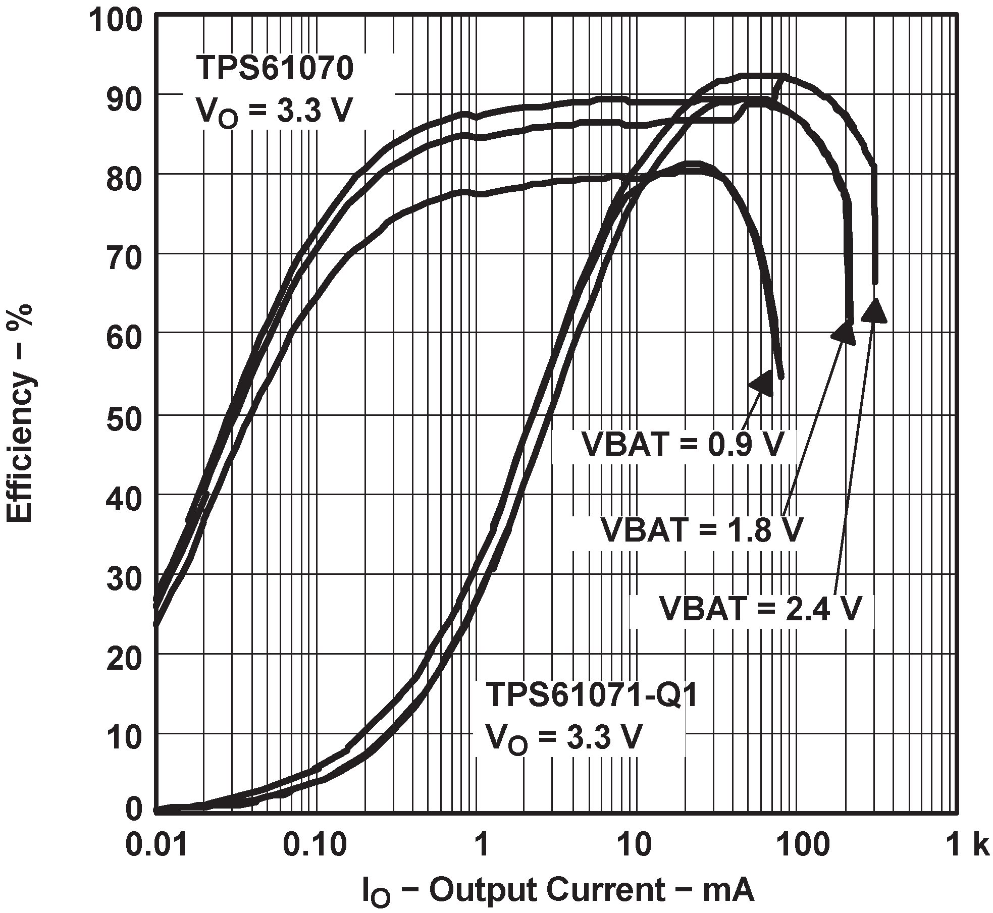 Figure 3. Efficiency vs Output Current
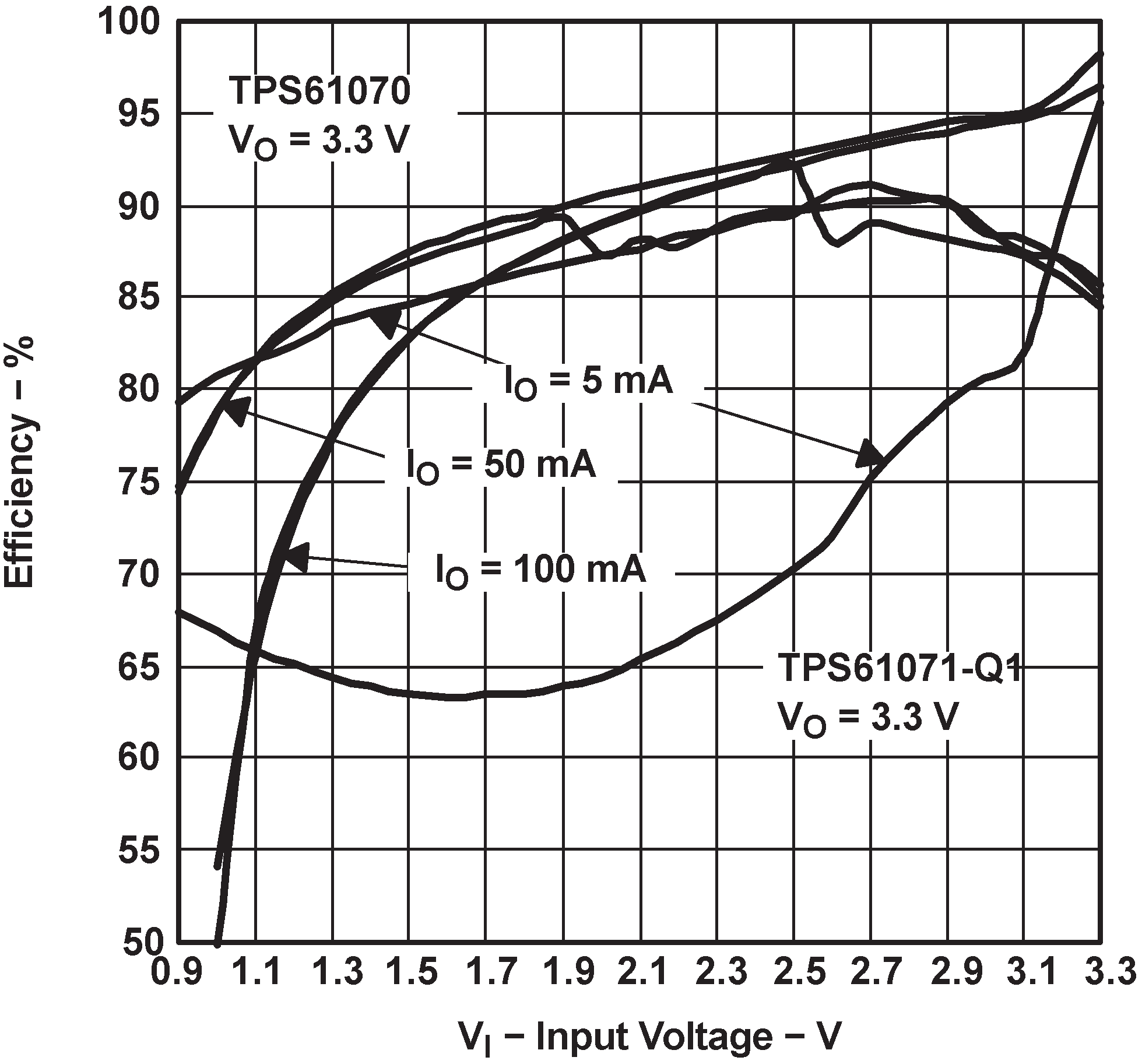 Figure 5. Efficiency vs Input Voltage
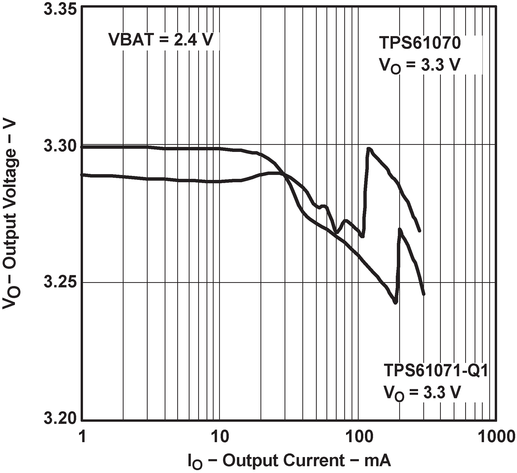 Figure 7. Output Voltage vs Output Current
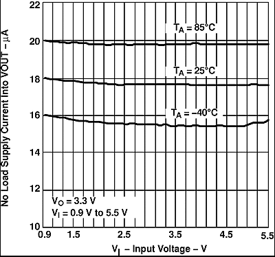 Figure 9. No Load Supply Current Into VOUT vs Input Voltage
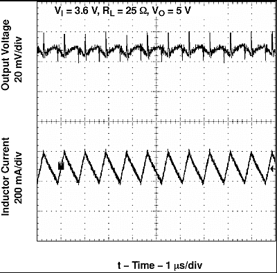 Figure 11. TPS61071 Output Voltage in Continuous Mode
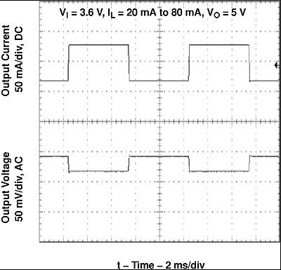 Figure 13. TPS61071 Load Transient Response
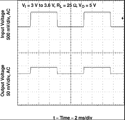 Figure 15. TPS61071 Line Transient Response
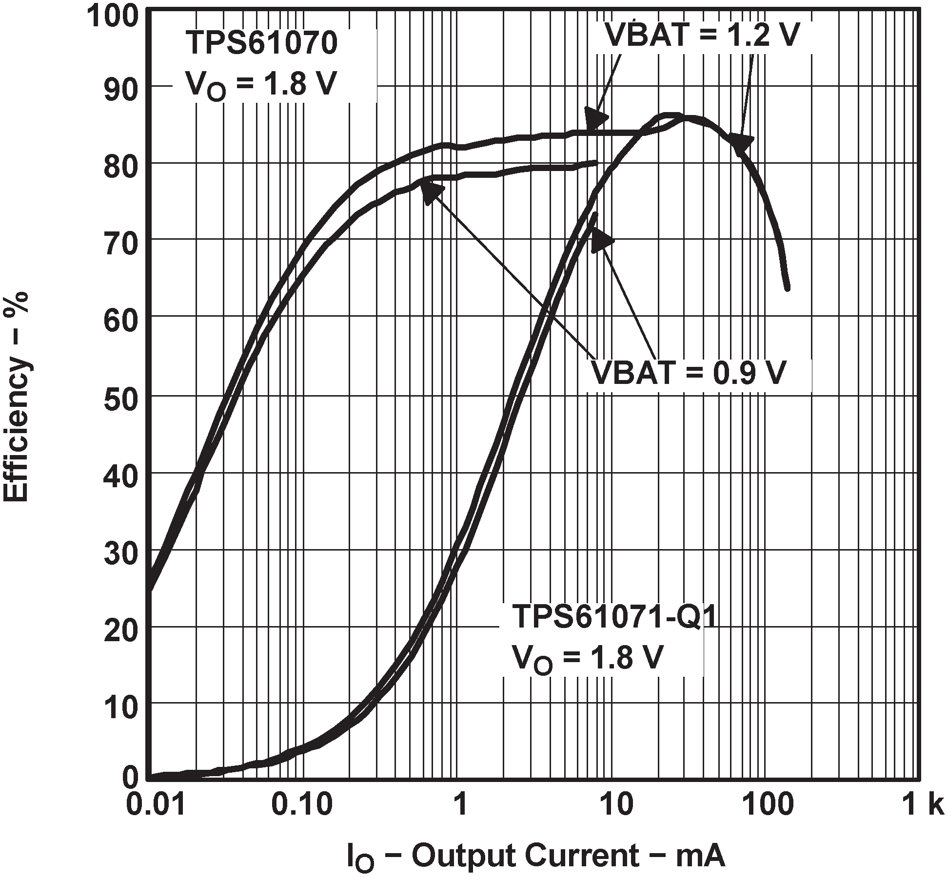 Figure 2. Efficiency vs Output Current
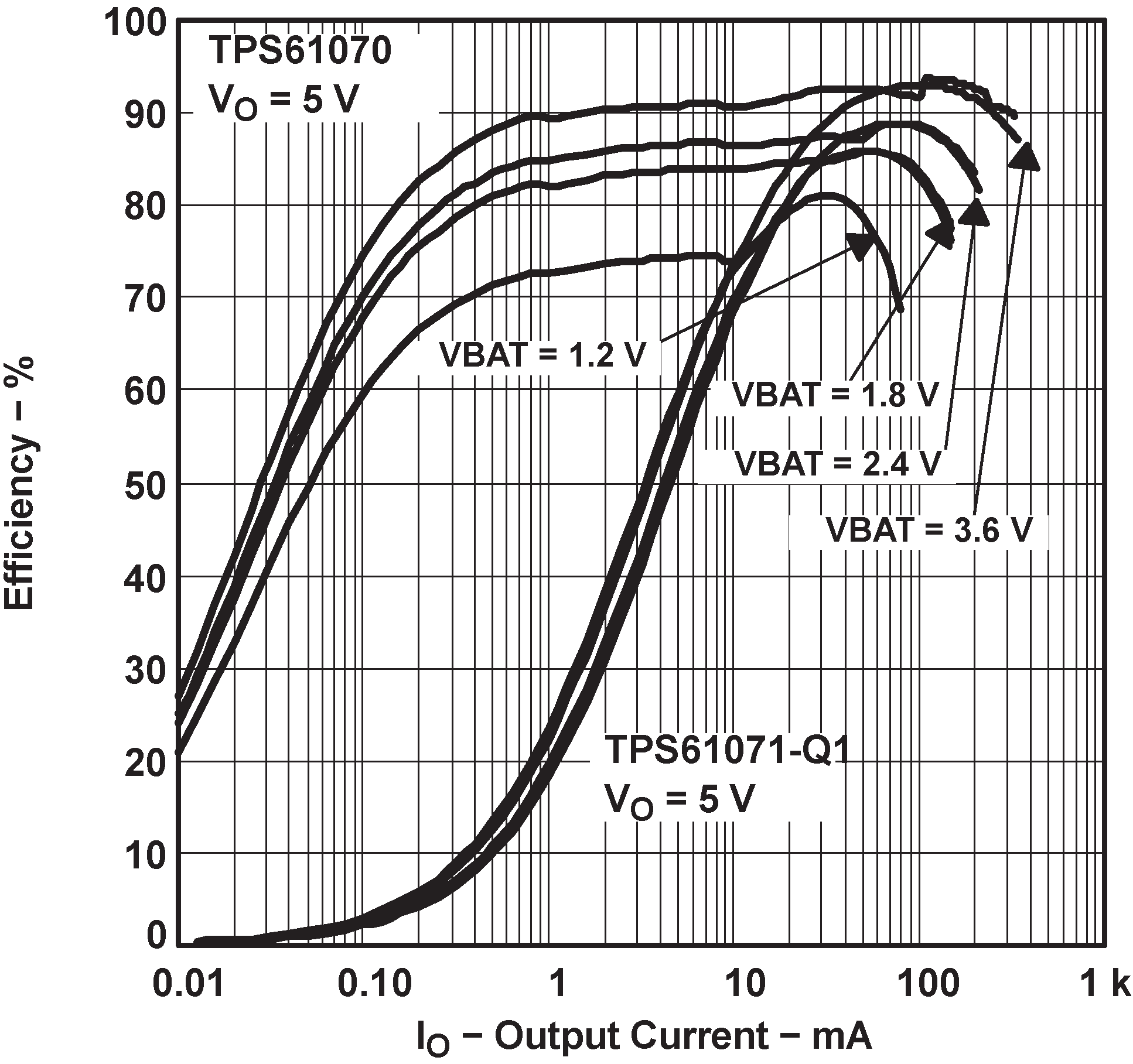 Figure 4. Efficiency vs Output Current
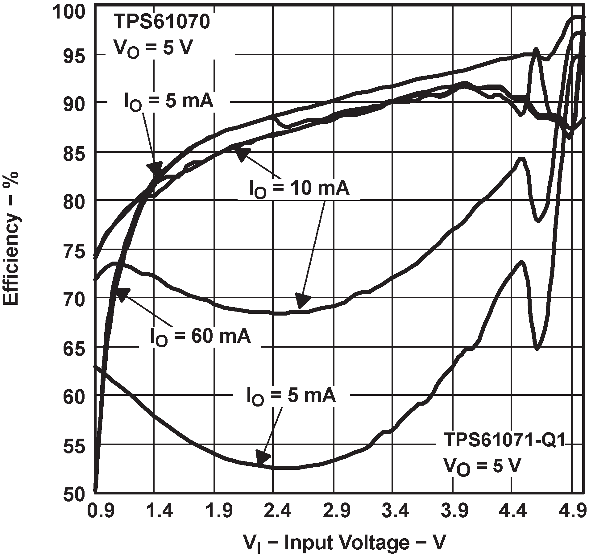 Figure 6. Efficiency vs Input Voltage
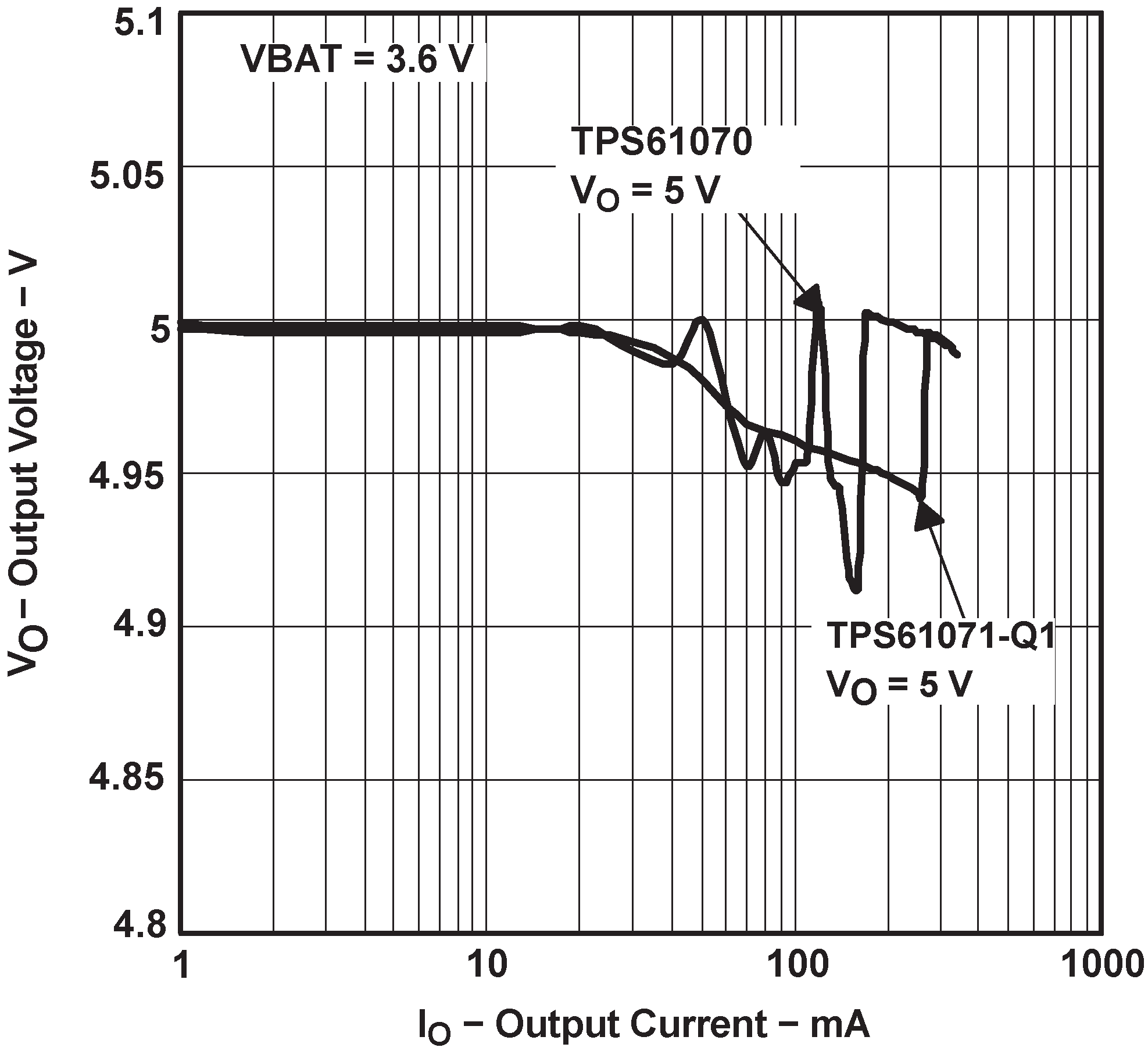 Figure 8. Output Voltage vs Output Current
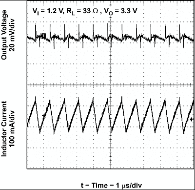 Figure 10. TPS61071 Output Voltage in Continuous Mode
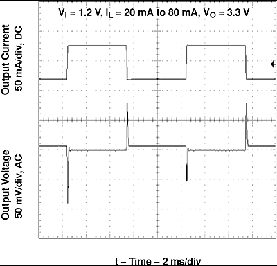 Figure 12. TPS61071 Load Transient Response
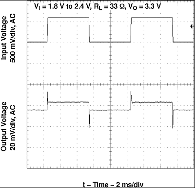 Figure 14. TPS61071 Line Transient Response
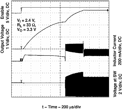 Figure 16. TPS61071 Start-Up After Enable
7 Detailed Description
7.1 Overview
The TPS61071-Q1 provides a boost power supply solution for products powered by either DC supply rails or batteries such as one-cell, two-cell, or three-cell alkaline, NiCd or NiMH, or one-cell Li-ion or Li-polymer battery. Output currents can go as high as 75 mA, while using a single-cell alkaline, and discharge down to 0.9 V. The device can also generate 5 V at 200 mA from a 3.3-V rail or a Li-ion battery. The boost converter is based on a fixed frequency, pulse-width modulation (PWM) controller using a synchronous rectifier to obtain maximum efficiency. The TPS61071-Q1 does not have a POWER-SAVE mode. Even with low-load currents, the device is forced to operate at the fixed switching frequency. The maximum peak current in the boost switch is limited typically to a value of 600 mA. An external-resistor divider programs the output voltage. To minimize battery drain, disable the converter. During shutdown, the load disconnects from the battery.
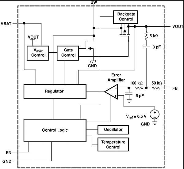
7.2 Functional Block Diagram
7.3 Feature Description
7.3.1 Controller Circuit
The controller circuit of the device is based on a fixed-frequency multiple feed-forward controller topology. Input voltage, output voltage, and voltage drop on the NMOS switch are monitored and forwarded to the regulator. So, changes in the operating conditions of the converter directly affect the duty cycle and must not take the indirect and slow way through the control loop and the error amplifier. The control loop, determined by the error amplifier, only has to handle small signal errors. The input for it is the feedback voltage on the FB pin. It is compared with the internal reference voltage to generate an accurate and stable output voltage.
The peak current of the NMOS switch is also sensed to limit the maximum current flowing through the switch and the inductor. The typical peak-current limit is set to 600 mA. An internal temperature sensor prevents the device from getting overheated in case of excessive power dissipation.
7.3.1.1 Synchronous Rectifier
The device integrates an N-channel and a P-channel MOSFET transistor to realize a synchronous rectifier. Because the commonly used discrete Schottky rectifier is replaced with a low RDS(on) PMOS switch, the power conversion efficiency reaches values above 90%. A special circuit is applied to disconnect the load from the input during shutdown of the converter. In conventional synchronous rectifier circuits, the backgate diode of the high-side PMOS is forward biased in shutdown and allows current flowing from the battery to the output. However, this device uses a special circuit, which takes the cathode of the backgate diode of the high-side PMOS and disconnects it from the source when the regulator is not enabled (EN = low).
The benefit of this feature for the system design engineer is that the battery is not depleted during shutdown of the converter. No additional components must be added to the design to make sure that the battery is disconnected from the output of the converter.
7.3.1.2 Undervoltage Lockout
An undervoltage lockout function prevents the device from operating if the supply voltage on VBAT is lower than approximately 0.8 V. When in operation and the battery is being discharged, the device automatically enters the shutdown mode if the voltage on VBAT drops below approximately 0.8 V. This undervoltage lockout function is implemented in order to prevent the malfunctioning of the converter.
7.3.1.3 Soft Start and Short-Circuit Protection
When the device enables, the internal start-up cycle starts with the first step, the precharge phase. During precharge, the rectifying switch is turned on until the output capacitor is charged to a value close to the input voltage. The rectifying switch is current limited during this phase. The current limit increases with the output voltage. This circuit also limits the output current under short-circuit conditions at the output. Figure 18 shows the typical precharge current vs output voltage for specific input voltages:
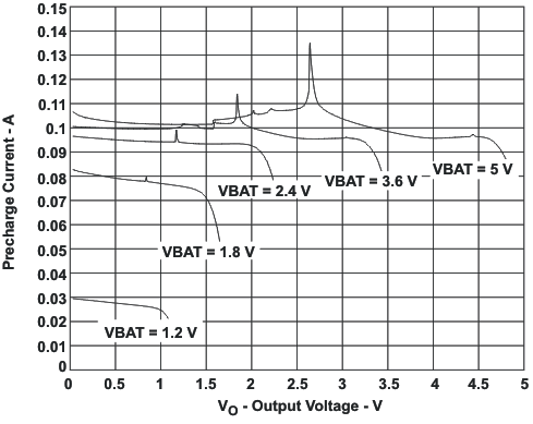 Figure 18. Precharge and Short Circuit Current
After charging the output capacitor to the input voltage, the device starts switching. If the input voltage is below 1.8 V, the device works with a fixed duty cycle of 70% until the output voltage reaches 1.8 V. After that the duty cycle is set depending on the input output voltage ratio. Until the output voltage reaches its nominal value, the boost switch current limit is set to 50% of its nominal value to avoid high peak currents at the battery during start-up. As soon as the output voltage is reached, the regulator takes control, and the switch current limit is set back to 100%.
7.4 Device Functional Modes
7.4.1 Device Enable
The device is put into operation when EN is set high and put into a SHUTDOWN mode when EN is set to GND. In SHUTDOWN mode, the regulator stops switching, all internal control circuitry switches off, and the device isolates the load from the input (see Synchronous Rectifier). This also means that the output voltage can drop below the input voltage during shutdown. During start-up of the converter, the duty cycle and the peak current are limited to avoid high-peak currents drawn from the battery.
8 Application and Implementation
NOTE
Information in the following applications sections is not part of the TI component specification, and TI does not warrant its accuracy or completeness. TI’s customers are responsible for determining suitability of components for their purposes. Customers should validate and test their design implementation to confirm system functionality.
8.1 Application Information
The TPS61071-Q1 DC-DC converter is intended for systems powered by a single-cell, up to triple-cell alkaline, NiCd, NiMH battery with a typical terminal voltage between 0.9 V and 5.5 V. The TPS61071-Q1 device can also be used in systems powered by one-cell Li-ion or Li-polymer with a typical voltage between 2.5 V and 4.2 V. Additionally, any other voltage source with a typical output voltage between 0.9 V and 5.5 V can power systems where the TPS61071-Q1 is used. Due to the nature of boost converters, the output voltage regulation is only maintained when the input voltage applied is lower than the programmed output voltage.
8.2 Typical Applications
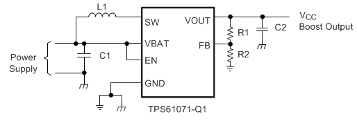 Figure 19. Typical Application Circuit
8.2.1 Design Requirements
In this example, TPS61071-Q1 is used to design a 3.3-V power supply with 75-mA output current capability supplied with an input voltage range from 0.9 V to 1.65 V.
8.2.2 Detailed Design Procedure
8.2.2.1 Programming the Output Voltage
The output voltage can be adjusted with an external resistor divider. The typical value of the voltage at the FB pin is 500 mV. The maximum recommended value for the output voltage is 5.5 V. The current through the resistive divider should be about 100 times greater than the current into the FB pin. The typical current into the FB pin is 0.01 µA, and the voltage across R2 is typically 500 mV. Based on those two values, the recommended value for R2 should be lower than 500 kΩ, in order to set the divider current at 1 µA or higher. Because of internal compensation circuitry, the value for this resistor should be in the range of 200 kΩ. From that, the value of resistor R1, depending on the needed output voltage (VO), is calculated using Equation 1:

For example, if an output voltage of 3.3 V is needed, a 1 MΩ resistor should be chosen for R1. If for any reason the value chosen for R2 is significantly lower than 200 kΩ, additional capacitance in parallel to R1 is recommended, if the device shows unstable regulation of the output voltage. The required capacitance value is calculated using Equation 2:

8.2.2.2 Inductor Selection L1
A boost converter normally requires two main passive components for storing energy during the conversion. A boost inductor and a storage capacitor at the output are required. To select the boost inductor, it is recommended to keep the possible peak inductor current below the current limit threshold of the power switch in the chosen configuration. For example, the current limit threshold of the TPS61071-Q1's switch is 600 mA. The highest peak current through the inductor and the switch depends on the output load, the input (VBAT), and the output voltage (VOUT). Estimation of the maximum average inductor current is done using Equation 3:

For example, for an output current of 75 mA at 3.3 V, at least 340 mA of average current flows through the inductor at a minimum input voltage of 0.9 V.
The second parameter for choosing the inductor is the desired current ripple in the inductor. Normally, it is advisable to work with a ripple of less than 20% of the average inductor current. A smaller ripple reduces the magnetic hysteresis losses in the inductor, as well as output voltage ripple and EMI. But in the same way, regulation time rises at load changes. In addition, a larger inductor increases the total system costs. With these parameters, it is possible to calculate the value for the inductor by using Equation 4:

Parameter f is the switching frequency and ΔIL is the ripple current in the inductor, i.e., 40% ΔIL. In this example, the desired inductor has the value of 4 µH. With this calculated value and the calculated currents, it is possible to choose a suitable inductor. In typical applications, a 4.7-µH inductance is recommended. The device has been optimized to operate with inductance values between 2.2 µH and 10 µH. Nevertheless, operation with higher inductance values may be possible in some applications. Detailed stability analysis is then recommended. Care must be taken because load transients and losses in the circuit can lead to higher currents as estimated in Equation 4. Also, the losses in the inductor caused by magnetic hysteresis losses and copper losses are a major parameter for total circuit efficiency.
Table 2 lists the inductor series from different suppliers which have been used with TPS6107x converters:
Table 2. List of Inductors
| VENDOR | INDUCTOR SERIES |
|---|---|
| TDK | VLF3010 |
| VLF4012 | |
| Wurth Elektronik | 744031xxx |
| 744042xxx | |
| EPCOS | B82462-G4 |
| Cooper Electronics Technologies | SD18 |
| SD20 | |
| Taiyo Yuden | CB2016B xxx |
| CB2518B xxx |
8.2.2.3 Capacitor Selection
8.2.2.3.1 Input Capacitor C1
TI recommends at least a 10-µF capacitor to improve transient behavior of the regulator and EMI behavior of the total power supply circuit. A ceramic capacitor or a tantalum capacitor with a 100-nF ceramic capacitor in parallel, placed close to the device, is recommended.
8.2.2.3.2 Output Capacitor C2
The major parameter necessary to define the output capacitor is the maximum allowed output voltage ripple of the converter. This ripple is determined by two parameters of the capacitor, the capacitance and the ESR. To calculate the minimum capacitance needed for the defined ripple, suppose that the ESR is zero and use Equation 5:

where
- Parameter f is the switching frequency and ΔV is the maximum allowed ripple.
With a chosen ripple voltage of 10 mV, a minimum capacitance of 4.5 µF is needed. In this value range, ceramic capacitors are a good choice. The ESR and the additional ripple created are negligible. It is calculated using Equation 6:

The total ripple is the sum of the ripple caused by the capacitance and the ripple caused by the ESR of the capacitor. Additional ripple is caused by load transients. This means that the output capacitor has to completely supply the load during the charging phase of the inductor. The value of the output capacitance depends on the speed of the load transients and the load current during the load change. With the calculated minimum value of 4.5 µF and load transient considerations, the recommended output capacitance value is in a 10 µF range.
Care must be taken on capacitance loss caused by derating due to the applied dc voltage and the frequency characteristic of the capacitor. For example, larger form factor capacitors (in 1206 size) have their self resonant frequencies in the same frequency range as the TPS61071-Q1 operating frequency. So the effective capacitance of the capacitors used may be significantly lower. Therefore, the recommendation is to use smaller capacitors in parallel instead of one larger capacitor.
8.2.2.4 Small Signal Stability
To analyze small signal stability in more detail, the small signal transfer function of the error amplifier and the regulator, which is given in Equation 7, can be used:

8.2.3 Application Curves


8.3 System Examples
 Figure 29. Power Supply Solution Having Small Total Solution Size
List of Components:
U1 = TPS61070DDC
L1 = 4.7 µH Taiyo Yuden CB2016B4R7M
c1 = 1 × 4.7 µF, 0603, X7R/X5R Ceramic
C2 = 2 × 4.7 µF, 0603, X7R/X5R Ceramic
 Figure 30. Power Supply Solution for Powering White LEDs in Lighting Applications
List of Components:
U1 = TPS61070DDC
L1 = 4.7 µH Taiyo Yuden CB2016B4R7M
c1 = 1 × 4.7 µF, 0603, X7R/X5R Ceramic
C2 = 2 × 4.7 µF, 0603, X7R/X5R Ceramic
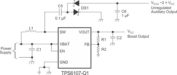 Figure 31. Power Supply Solution With Auxiliary Positive Output Voltage
List of Components:
U1 = TPS61070DDC
L1 = 4.7 µH Wurth Elektronik 744031004
c1 = 2 × 4.7 µF, 0603, X7R/X5R Ceramic
C2 = 2 × 4.7 µF, 0603, X7R/X5R Ceramic
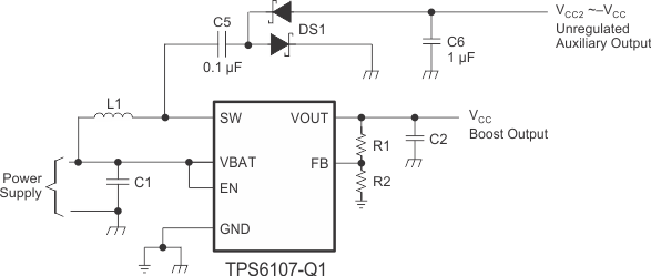 Figure 32. Power Supply Solution With Auxiliary Negative Output Voltage
List of Components:
U1 = TPS61070DDC
L1 = 4.7 µH Wurth Elektronik 744031004
c1 = 2 × 4.7 µF, 0603, X7R/X5R Ceramic
C2 = 2 × 4.7 µF, 0603, X7R/X5R Ceramic
9 Power Supply Recommendations
The TPS61071-Q1 is designed to operate from an input voltage-supply range between 0.9 V and 5.5 V. The power supply can be a DC-supply rail or one-cell, two-cell, or three-cell alkaline, NiCd or NiMH, or one-cell Li-Ion or Li-Polymer battery. The input supply should be well regulated with the rating of TPS61071-Q1. If the input supply is located more than a few inches from the device, additional bulk capacitance may be required in addition to the ceramic bypass capacitors. An electrolytic or tantalum capacitor with a value of 47 μF is a typical choice.
10 Layout
10.1 Layout Guidelines
As for all switching power supplies, the layout is an important step in the design, especially at high-peak currents and high switching frequencies. If the layout is not carefully done, the regulator could show stability problems as well as EMI problems. Therefore, use wide and short traces for the main current path and for the power ground tracks. The input capacitor, output capacitor, and the inductor should be placed as close as possible to the device. Use a common ground node for power ground and a different one for control ground to minimize the effects of ground noise. Connect these ground nodes at any place close to the ground pin of the device.
The feedback divider should be placed as close as possible to the ground pin of the device. To lay out the control ground, it is recommended to use short traces as well, separated from the power ground traces. This avoids ground shift problems, which can occur due to superimposition of power ground current and control ground current.
10.2 Layout Example
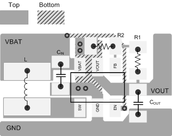 Figure 33. PCB Layout
10.3 Thermal Considerations
Implementation of integrated circuits in low-profile and fine-pitch surface-mount packages typically requires special attention to power dissipation. Many system-dependent issues such as thermal coupling, airflow, added heat sinks and convection surfaces, and the presence of other heat-generating components affect the power-dissipation limits of a given component.
There are three basic approaches for enhancing thermal performance.
- Improving the power dissipation capability of the PCB design
- Improving the thermal coupling of the component to the PCB
- Introducing airflow in the system
The maximum recommended junction temperature (TJ) of the TPS61071-Q1 device is 125°C. The thermal resistance of the 6-pin thin SOT package (DDC) is RθJA = 130°C/W. Specified regulator operation is assured to a maximum ambient temperature TA of 85°C. Therefore, the maximum power dissipation is about 308 mW. More power can be dissipated if the maximum ambient temperature of the application is lower.

11 Device and Documentation Support
11.1 Device Support
11.1.1 Third-Party Products Disclaimer
TI'S PUBLICATION OF INFORMATION REGARDING THIRD-PARTY PRODUCTS OR SERVICES DOES NOT CONSTITUTE AN ENDORSEMENT REGARDING THE SUITABILITY OF SUCH PRODUCTS OR SERVICES OR A WARRANTY, REPRESENTATION OR ENDORSEMENT OF SUCH PRODUCTS OR SERVICES, EITHER ALONE OR IN COMBINATION WITH ANY TI PRODUCT OR SERVICE.
11.2 Community Resources
The following links connect to TI community resources. Linked contents are provided "AS IS" by the respective contributors. They do not constitute TI specifications and do not necessarily reflect TI's views; see TI's Terms of Use.
-
TI E2E™ Online Community TI's Engineer-to-Engineer (E2E) Community. Created to foster collaboration among engineers. At e2e.ti.com, you can ask questions, share knowledge, explore ideas and help solve problems with fellow engineers.
-
Design Support TI's Design Support Quickly find helpful E2E forums along with design support tools and contact information for technical support.
11.3 Trademarks
E2E is a trademark of Texas Instruments.
All other trademarks are the property of their respective owners.
11.4 Electrostatic Discharge Caution

These devices have limited built-in ESD protection. The leads should be shorted together or the device placed in conductive foam during storage or handling to prevent electrostatic damage to the MOS gates.
11.5 Glossary
SLYZ022 — TI Glossary.
This glossary lists and explains terms, acronyms, and definitions.
12 Mechanical, Packaging, and Orderable Information
The following pages include mechanical, packaging, and orderable information. This information is the most current data available for the designated devices. This data is subject to change without notice and revision of this document. For browser-based versions of this data sheet, refer to the left-hand navigation.
