SLVAEW5 August 2020 – MONTH TPS22990
Tech Note
High-speed, low-power memory banks and processors are becoming more common with innovation in Smartphones, 5G, IoT, automotive infotainment, and ADAS. As the trend towards low-voltage rails continues, finding a switching solution that can operate from input voltages below 1.8 V is imperative. When a system calls for specific power distribution, power sequencing, or power savings, a load switch can be used to meet these specific timing or power savings requirements.
A load switch is a device that passes power from the supply to the load. The key benefits of using an integrated load switch when input voltage is less than 1.5 V are that the load switch maintains low on-resistance, reduces BOM count, and provides additional integrated features, as shown in Table 1-1. This document presents three switching solutions and explains how an integrated load switch optimizes low-input voltage applications.
| VIN < 1.5 V |
Low RDS(on) |
Integrated Features | BOM Count |
|
|---|---|---|---|---|
| TI Integrated Load Switch | ✓ |
✓ |
✓ | 1 |
| Discrete PMOS | ✗ |
✗ |
✗ | 6+ |
| Discrete NMOS | ✓ | ✓ | ✗ | 3+ |
Discrete MOSFET Solutions
The simplest and most common discrete power-switching solutions use a PMOS transistor to pass power from input to output. As shown in Figure 1, the enable signal drives the pass FET gate while the input voltage is tied to the pass FET source. To turn on the FET, the enable signal must be pulled low. When the active low-enable signal is activated, the FET turns on and the load connects to the input voltage supply.
 Figure 1-1 Discrete PMOS Switch
One of the drawbacks of using a PMOS transistor, is the transistor does not perform well in low input voltage applications. For the PMOS to turn on, the gate-to-source voltage must be less than the threshold voltage (VGS < VTH ). When VGS is close in value to VTH, the FET partially turns on. With the pass FET not fully on, the device on-resistance (RDS(on)) is very high. The resulting large voltage drop and high-power dissipation across the FET leads to reduced efficiency and thermal management concerns.
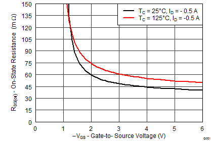
For example, consider the TI PMOS device, CSD23202W10, that has a threshold voltage of VTH = –0.6 V. By applying 0.65 V at the input of the CSD23202W10, the application limits the maximum VGS to –0.65 V, and the FET only turns on partially. Figure 2 shows the corresponding exponential increase in RDS(on) when the input voltage is less than 1.5 V.
 Figure 1-2 On-Resistance vs. VGS for
CSD23202W10
 While the CSD23202W10 is a switching solution with good performance metrics when input voltage is greater than 1.5 V, it is not ideal for low-input voltage applications. Even with various configurations of additional resistors, capacitors, and NMOS transistors, the discrete PMOS solution continues to have diminished performance at lower input voltages.
The second type of switching solution uses an NMOS transistor as the main power switch. To turn on an NMOS, the gate-to-source voltage must be higher than the threshold voltage (VGS > VTH). To meet this condition, the gate voltage is raised above the input voltage through a higher voltage rail within the system or a charge pump, as shown in Figure 3. The active high-gate voltage ensures that even low-input voltage can pass through the switch while also maintaining a low on-resistance.
VG = N · Input Voltage

However, the additional required components lead to a larger PCB footprint, increased BOM count, and higher cost. While this tech note only covers two discrete solutions, the application report Integrated Load Switches Versus Discrete MOSFETs compares the performance of numerous discrete switching solutions with the integrated load switch.
Achieve Optimal Low Voltage Performance Using Integrated Load Switches
When compared with discrete switching solutions, integrated load switches maintain a constant RDS(on) across a spectrum of input voltages without added circuit complexity, which contributes to reduced solution size and cost savings. On-resistance is maintained across the entire input voltage range due to the inclusion of a bias voltage, VBIAS, which is higher than the input voltage to provide power to run the internal functions of the device.
For example, Table 1-2 shows different load switch options that support input voltages as low as 0.6 V while maintaining a steady RDS(on) at room temperature.
| Device | Input Voltage Range (V) | RDS(on) (mΩ) | Channel Count | VBIAS | |
|---|---|---|---|---|---|
| MIN | MAX | ||||
| TPS22990 | 0.6 | 5.5 | 3.9 | Single | ✓ |
| TPS22975 | 5.7 | 16 | Single | ✓ | |
| TPS22976 | 14 | Dual | ✓ | ||
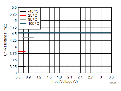
Sustaining low on-resistance reduces the voltage drop across the device, ensuring that all the input voltage is transmitted to the load. Therefore, load switches maintain high efficiency and performance regardless of low VIN. Figure 4 illustrates the constant on-resistance the TPS22990 maintains across the entire input voltage range at different temperatures. In contrast, PMOS solutions such as the CSD23202W10 experience an exponential increase in RDS(on) when used as a load switch at lower input voltages.
 Figure 1-4 On-Resistance vs. VIN for TPS22990
 Integrated load switches also provide additional features not available with discrete switching solutions such as quick output discharge, configurable rise time, and thermal shutdown. Common design challenges and how to solve them with integrated power switches are further addressed in 11 Ways to Protect Your Power Path.
Conclusion
As industry develops more processors and memory banks with lower core voltage and I/O rails, low input voltage switching solutions contribute to power management across various end equipments. Integrated load switches optimize power performance by maintaining low on-resistance and incorporating additional features that fine-tune efficiency. Integrated load switch options that enhance power distribution and savings in low-input voltage applications can be found on the TI.com portal at Load Switches.