-
ISO5452-Q1 High-CMTI 2.5-A and 5-A Isolated IGBT, MOSFET Gate Driver With Split Outputs and Active Protection Features
- 1 Features
- 2 Applications
- 3 Description
- 4 Revision History
- 5 Description (continued)
- 6 Pin Configuration and Function
-
7 Specifications
- 7.1 Absolute Maximum Ratings
- 7.2 ESD Ratings
- 7.3 Recommended Operating Conditions
- 7.4 Thermal Information
- 7.5 Power Ratings
- 7.6 Insulation Specifications
- 7.7 Safety-Related Certifications
- 7.8 Safety Limiting Values
- 7.9 Electrical Characteristics
- 7.10 Switching Characteristics
- 7.11 Insulation Characteristics Curves
- 7.12 Typical Characteristics
- 8 Parameter Measurement Information
- 9 Detailed Description
-
10Application and Implementation
- 10.1 Application Information
- 10.2
Typical Applications
- 10.2.1 Design Requirements
- 10.2.2
Detailed Design Procedure
- 10.2.2.1 Recommended ISO5452-Q1 Application Circuit
- 10.2.2.2 FLT and RDY Pin Circuitry
- 10.2.2.3 Driving the Control Inputs
- 10.2.2.4 Local Shutdown and Reset
- 10.2.2.5 Global-Shutdown and Reset
- 10.2.2.6 Auto-Reset
- 10.2.2.7 DESAT Pin Protection
- 10.2.2.8 DESAT Diode and DESAT Threshold
- 10.2.2.9 Determining the Maximum Available, Dynamic Output Power, POD-max
- 10.2.2.10 Example
- 10.2.2.11 Higher Output Current Using an External Current Buffer
- 10.2.3 Application Curves
- 11Power Supply Recommendations
- 12Layout
- 13Device and Documentation Support
- 14Mechanical, Packaging, and Orderable Information
- IMPORTANT NOTICE
ISO5452-Q1 High-CMTI 2.5-A and 5-A Isolated IGBT, MOSFET Gate Driver With Split Outputs and Active Protection Features
1 Features
- Qualified for Automotive Applications
- AEC-Q100 Qualified With the Following Results:
- Device Temperature Grade 1: –40°C to +125°C Ambient Operating Temperature Range
- Device HBM Classification Level 3A
- Device CDM Classification Level C6
- 50-kV/μs Minimum and 100-kV/μs Typical Common-Mode Transient Immunity (CMTI)
at VCM = 1500 V - Split Outputs to provide 2.5-A Peak Source and
5-A Peak Sink Currents - Short Propagation Delay: 76 ns (Typ),
110 ns (Max) - 2-A Active Miller Clamp
- Output Short-Circuit Clamp
- Soft Turn-Off (STO) during Short Circuit
- Fault Alarm upon Desaturation Detection is Signaled on FLT and Reset Through RST
- Input and Output Undervoltage Lockout (UVLO) With Ready (RDY) Pin Indication
- Active Output Pulldown and Default Low Outputs With Low Supply or Floating Inputs
- 2.25-V to 5.5-V Input Supply Voltage
- 15-V to 30-V Output Driver Supply Voltage
- CMOS Compatible Inputs
- Rejects Input Pulses and Noise Transients Shorter Than 20 ns
- Isolation Surge Withstand Voltage 10000-VPK
- Safety-Related Certifications:
- 8000-VPK VIOTM and 1420-VPK VIORM Reinforced Isolation per DIN V VDE V 0884-10 (VDE V 0884-10):2006-12
- 5700-VRMS Isolation for 1 Minute per UL 1577
- CSA Component Acceptance Notice 5A, IEC 60950–1 and IEC 60601–1 End Equipment Standards
- TUV Certification per EN 61010-1 and EN 60950-1
- GB4943.1-2011 CQC Certification
- All Certifications Complete
2 Applications
- Isolated IGBT and MOSFET Drives in:
- HEV and EV Power Modules
- Industrial Motor Control Drives
- Industrial Power Supplies
- Solar Inverters
- Induction Heating
3 Description
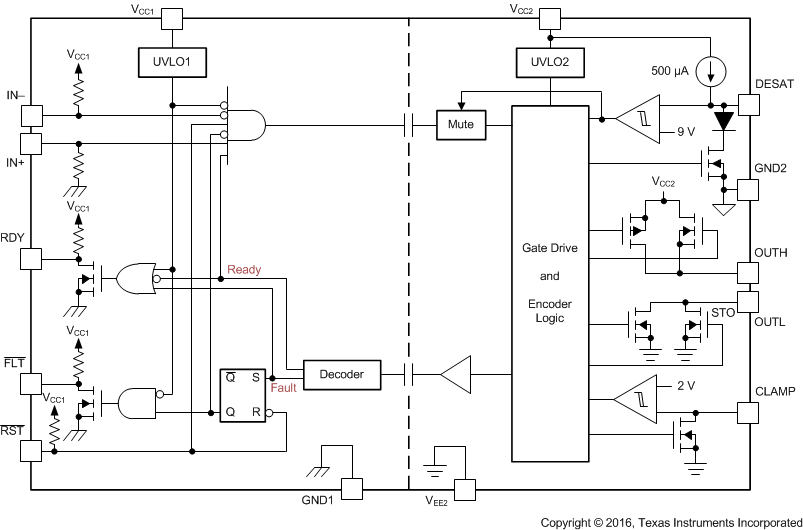
The ISO5452-Q1 is a 5.7-kVRMS, reinforced isolated gate driver for IGBTs and MOSFETs with split outputs, OUTH and OUTL, providing 2.5-A source and 5-A sink current. The input side operates from a single 2.25-V to 5.5-V supply. The output side allows for a supply range from minimum 15 V to maximum
30 V. Two complementary CMOS inputs control the output state of the gate driver. The short propagation time of 76 ns assures accurate control of the output stage.
An internal desaturation (DESAT) fault detection recognizes when the IGBT is in an overcurrent condition. Upon a DESAT detect, a Mute logic immediately blocks the output of the isolator and initiates a soft-turn-off procedure which disables OUTH, and pulls OUTL to low over a time span of
2 μs. When OUTL reaches 2 V with respect to the most negative supply potential, VEE2, the gate driver output is pulled hard to VEE2 potential, turning the IGBT immediately off.
Device Information(1)
| PART NUMBER | PACKAGE | BODY SIZE (NOM) |
|---|---|---|
| ISO5452-Q1 | SOIC (16) | 10.30 mm × 7.50 mm |
- For all available packages, see the orderable addendum at the end of the datasheet.
Functional Block Diagram
5 Description (continued)
When desaturation is active, a fault signal is sent across the isolation barrier, pulling the FLT output at the input side low and blocking the isolator input. Mute logic is activated through the soft-turn-off period. The FLT output condition is latched and can be reset only after RDY goes high, through a low-active pulse at the RST input.
When the IGBT is turned off during normal operation with bipolar output supply, the output is hard clamp to VEE2. If the output supply is unipolar, an active Miller clamp can be used, allowing Miller current to sink across a low impedance path, preventing IGBT to be dynamically turned on during high voltage transient conditions.
The readiness for the gate driver to be operated is under the control of two undervoltage-lockout circuits monitoring the input side and output side supplies. If either side has insufficient supply the RDY output goes low, otherwise this output is high.
The ISO5452-Q1 is available in a 16-pin SOIC package. Device operation is specified over a temperature range from –40°C to +125°C ambient.
6 Pin Configuration and Function
Pin Functions
| PIN | I/O | DESCRIPTION | |
|---|---|---|---|
| NO. | NAME | ||
| 1 | VEE2 | — | Output negative supply. Connect to GND2 for Unipolar supply application. |
| 2 | DESAT | I | Desaturation voltage input |
| 3 | GND2 | — | Gate drive common. Connect to IGBT emitter. |
| 4 | OUTH | O | Positive gate drive voltage output |
| 5 | VCC2 | — | Most positive output supply potential. |
| 6 | OUTL | O | Negative gate drive voltage output |
| 7 | CLAMP | O | Miller clamp output |
| 8 | VEE2 | — | Output negative supply. Connect to GND2 for Unipolar supply application. |
| 9 | GND1 | — | Input ground |
| 10 | IN+ | I | Non-inverting gate drive voltage control input |
| 11 | IN– | I | Inverting gate drive voltage control input |
| 12 | RDY | O | Power-good output, active high when both supplies are good. |
| 13 | FLT | O | Fault output, low-active during DESAT condition |
| 14 | RST | I | Reset input, apply a low pulse to reset fault latch. |
| 15 | VCC1 | — | Positive input supply (2.25 V to 5.5 V) |
| 16 | GND1 | — | Input ground |
7 Specifications
7.1 Absolute Maximum Ratings
over operating free-air temperature range (unless otherwise noted)(1)| MIN | MAX | UNIT | ||||
|---|---|---|---|---|---|---|
| VCC1 | Supply voltage input side | GND1 – 0.3 | 6 | V | ||
| VCC2 | Positive supply voltage output side | (VCC2 – GND2) | –0.3 | 35 | V | |
| VEE2 | Negative supply voltage output side | (VEE2 – GND2) | –17.5 | 0.3 | V | |
| V(SUP2) | Total supply output voltage | (VCC2 – VEE2) | –0.3 | 35 | V | |
| V(OUTH) | Positive gate driver output voltage | VEE2 – 0.3 | VCC2 + 0.3 | V | ||
| V(OUTL) | Negative gate driver output voltage | VEE2 – 0.3 | VCC2 + 0.3 | V | ||
| I(OUTH) | Gate driver high output current | Gate driver high output current (maximum pulse width = 10 μs, maximum duty cycle = 0.2%) |
2.7 | A | ||
| I(OUTL) | Gate driver low output current | Gate driver high output current (maximum pulse width = 10 μs, maximum duty cycle = 0.2%) |
5.5 | A | ||
| V(LIP) | Voltage at IN+, IN–, FLT, RDY, RST | GND1 - 0.3 | VCC1 + 0.3 | V | ||
| I(LOP) | Output current of FLT, RDY | 10 | mA | |||
| V(DESAT) | Voltage at DESAT | GND2 - 0.3 | VCC2 + 0.3 | V | ||
| V(CLAMP) | Clamp voltage | VEE2 – 0.3 | VCC2 + 0.3 | V | ||
| TJ | Junction temperature | –40 | 150 | °C | ||
| TSTG | Storage temperature | –65 | 150 | °C | ||
7.2 ESD Ratings
| VALUE | UNIT | |||
|---|---|---|---|---|
| V(ESD) | Electrostatic discharge | Human-body model (HBM), per AEC Q100-002(1) | ±4000 | V |
| Charged-device model (CDM), per AEC Q100-011 | ±1500 | |||
7.3 Recommended Operating Conditions
over operating free-air temperature range (unless otherwise noted)| MIN | NOM | MAX | UNIT | ||
|---|---|---|---|---|---|
| VCC1 | Supply voltage input side | 2.25 | 5.5 | V | |
| VCC2 | Positive supply voltage output side (VCC2 – GND2) | 15 | 30 | V | |
| VEE2 | Negative supply voltage output side (VEE2 – GND2) | –15 | 0 | V | |
| V(SUP2) | Total supply voltage output side (VCC2 – VEE2) | 15 | 30 | V | |
| VIH | High-level input voltage (IN+, IN–, RST) | 0.7 × VCC1 | VCC1 | V | |
| VIL | Low-level input voltage (IN+, IN–, RST) | 0 | 0.3 × VCC1 | V | |
| tUI | Pulse width at IN+, IN– for full output (CLOAD = 1 nF) | 40 | ns | ||
| tRST | Pulse width at RST for resetting fault latch | 800 | ns | ||
| TA | Ambient temperature | –40 | 125 | °C | |
7.4 Thermal Information
| THERMAL METRIC(1) | ISO5452-Q1 | UNIT | |
|---|---|---|---|
| DW (SOIC) | |||
| 16 PINS | |||
| RθJA | Junction-to-ambient thermal resistance | 99.6 | °C/W |
| RθJC(top) | Junction-to-case (top) thermal resistance | 48.5 | °C/W |
| RθJB | Junction-to-board thermal resistance | 56.5 | °C/W |
| ψJT | Junction-to-top characterization parameter | 29.2 | °C/W |
| ψJB | Junction-to-board characterization parameter | 56.5 | °C/W |
7.5 Power Ratings
VCC1 = 5.5 V, VCC2 = 30 V, TA = 25°C| PARAMETER | TEST CONDITIONS | MIN | TYP | MAX | UNIT | |
|---|---|---|---|---|---|---|
| PD | Maximum power dissipation(1) | 1255 | mW | |||
| PID | Maximum input power dissipation | 175 | mW | |||
| POD | Maximum output power dissipation | 1080 | mW | |||
7.6 Insulation Specifications
| PARAMETER | TEST CONDITIONS | VALUE | UNIT | |
|---|---|---|---|---|
| GENERAL | ||||
| CLR | External clearance(1) | Shortest terminal-to-terminal distance through air | >8 | mm |
| CPG | External creepage(1) | Shortest terminal-to-terminal distance across the package surface | >8 | mm |
| DTI | Distance through the insulation | Minimum internal gap (internal clearance) | >21 | μm |
| CTI | Tracking resistance (comparative tracking index) | DIN EN 60112 (VDE 0303-11); IEC 60112; | >600 | V |
| Material Group | According to IEC 60664-1; UL 746A | I | ||
| Overvoltage category (according to IEC 60664-1) | Rated Mains Voltage ≤ 300 VRMS | I-IV | ||
| Rated Mains Voltage ≤ 600 VRMS | I-III | |||
| Rated Mains Voltage ≤ 1000 VRMS | I-II | |||
| DIN V VDE V 0884-10 (VDE V 0884-10):2006-12(2) | ||||
| VIORM | Maximum repetitive peak isolation voltage | AC voltage (bipolar) | 1420 | VPK |
| VIOWM | Maximum isolation working voltage | AC voltage. Time dependent dielectric breakdown (TDDB) Test, see Figure 1 | 1000 | VRMS |
| DC voltage | 1420 | VDC | ||
| VIOTM | Maximum transient isolation voltage | VTEST = VIOTM, t = 60 s (qualification), t = 1 s (100% production) | 8000 | VPK |
| VIOSM | Maximum surge isolation voltage(3) | Test method per IEC 60065, 1.2/50 μs waveform, VTEST = 1.6 × VIOSM = 10000 VPK (qualification)(3) | 6250 | VPK |
| qpd | Apparent charge(4) | Method a: After I/O safety test subgroup 2/3, Vini = VIOTM, tini = 60 s; Vpd(m) = 1.2 × VIORM = 1704 VPK, tm = 10 s | ≤5 | pC |
| Method a: After environmental tests subgroup 1, Vini = VIOTM, tini = 60 s; Vpd(m) = 1.6 × VIORM = 2272 VPK, tm = 10 s | ≤5 | |||
| Method b1: At routine test (100% production) and preconditioning (type test), Vini = VIOTM, tini = 60 s; Vpd(m) = 1.875× VIORM = 2663 VPK, tm = 10 s | ≤5 | |||
| RIO | Isolation resistance, input to output(5) | VIO = 500 V, TA = 25°C | > 1012 | Ω |
| VIO = 500 V, 100°C ≤ TA ≤ 125°C | > 1011 | Ω | ||
| VIO = 500 V at TS = 150°C | > 109 | Ω | ||
| CIO | Barrier capacitance, input to output(5) | VIO = 0.4 x sin (2πft), f = 1 MHz | 1 | pF |
| Pollution degree | 2 | |||
| UL 1577 | ||||
| VISO | Withstanding Isolation voltage | VTEST = VISO, t = 60 s (qualification), VTEST = 1.2 × VISO = 6840 VRMS, t = 1 s (100% production) |
5700 | VRMS |
7.7 Safety-Related Certifications
| VDE | CSA | UL | CQC | TUV |
|---|---|---|---|---|
| Certified according to DIN V VDE V 0884-10 (VDE V 0884-10):2006-12 and DIN EN 60950-1 (VDE 0805 Teil 1):2011-01 |
Certified according to CSA Component Acceptance Notice 5A, IEC 60950-1 and IEC 60601-1 | Certified according to UL 1577 Component Recognition Program | Certified according to GB 4943.1-2011 | Certified according to EN 61010-1:2010 (3rd Ed) and EN 60950-1:2006/A11:2009/A1:2010/ A12:2011/A2:2013 |
| Reinforced Insulation Maximum Transient isolation voltage, 8000 VPK; Maximum surge isolation voltage, 6250 VPK, Maximum repetitive peak isolation voltage, 1420 VPK |
Isolation Rating of 5700 VRMS; Reinforced insulation per CSA 60950- 1- 07+A1+A2 and IEC 60950-1 (2nd Ed.), 800 VRMS max working voltage (pollution degree 2, material group I) ; 2 MOPP (Means of Patient Protection) per CSA 60601-1:14 and IEC 60601-1 Ed. 3.1, 250 VRMS (354 VPK) max working voltage |
Single Protection, 5700 VRMS (1) | Reinforced Insulation, Altitude ≤ 5000m, Tropical climate, 400 VRMS maximum working voltage | 5700 VRMS Reinforced insulation per EN 61010-1:2010 (3rd Ed) up to working voltage of 600 VRMS 5700 VRMS Reinforced insulation per EN 60950-1:2006/A11:2009/A1:2010/ A12:2011/A2:2013 up to working voltage of 800 VRMS |
| Certification completed Certificate number: 40040142 |
Master contract number: 220991 | Certification completed File number: E181974 |
Certification completed Certificate number: CQC16001141761 |
Certification completed Client ID number: 77311 |
7.8 Safety Limiting Values
Safety limiting intends to minimize potential damage to the isolation barrier upon failure of input or output circuitry. A failure of the I/O can allow low resistance to ground or the supply and, without current limiting, dissipate sufficient power to overheat the die and damage the isolation barrier, potentially leading to secondary system failures.| PARAMETER | TEST CONDITIONS | MIN | TYP | MAX | UNIT | |
|---|---|---|---|---|---|---|
| IS | Safety input, output or supply current | RθJA = 99.6°C/W, VI = 2.75 V, TJ = 150°C, TA = 25°C, see Figure 2 | 456 | mA | ||
| RθJA = 99.6°C/W, VI = 3.6 V, TJ = 150°C, TA = 25°C, see Figure 2 | 346 | |||||
| RθJA = 99.6°C/W, VI = 5.5 V, TJ = 150°C, TA = 25°C, see Figure 2 | 228 | |||||
| RθJA = 99.6°C/W, VI = 15 V, TJ = 150°C, TA = 25°C, see Figure 2 | 484 | |||||
| RθJA = 99.6°C/W, VI = 30 V, TJ = 150°C, TA = 25°C, see Figure 2 | 42 | |||||
| PS | Safety input, output, or total power | RθJA = 99.6°C/W, TJ = 150°C, TA = 25°C, see Figure 3 | 1255(1) | mW | ||
| TS | Safety temperature | 150 | °C | |||
The safety-limiting constraint is the maximum junction temperature specified in the data sheet. The power dissipation and junction-to-air thermal impedance of the device installed in the application hardware determines the junction temperature. The assumed junction-to-air thermal resistance in the Thermal Information table is that of a device installed on a high-K test board for leaded surface-mount packages. The power is the recommended maximum input voltage times the current. The junction temperature is then the ambient temperature plus the power times the junction-to-air thermal resistance.
7.9 Electrical Characteristics
Over recommended operating conditions unless otherwise noted.| PARAMETER | TEST CONDITIONS | MIN | TYP | MAX | UNIT | ||
|---|---|---|---|---|---|---|---|
| VOLTAGE SUPPLY | |||||||
| VIT+(UVLO1) | Positive-going UVLO1 threshold voltage input side (VCC1 – GND1) | 2.25 | V | ||||
| VIT-(UVLO1) | Negative-going UVLO1 threshold voltage input side (VCC1 – GND1) | 1.7 | V | ||||
| VHYS(UVLO1) | UVLO1 Hysteresis voltage (VIT+ – VIT–) input side | TA = 25°C, VCC1 = 5 V, VCC2 – GND2 = 15 V, GND2 – VEE2 = 8 V | 0.2 | V | |||
| VIT+(UVLO2) | Positive-going UVLO2 threshold voltage output side (VCC2 – GND2) | 13 | V | ||||
| TA = 25°C, VCC1 = 5 V, VCC2 – GND2 = 15 V, GND2 – VEE2 = 8 V | 12 | ||||||
| VIT-(UVLO2) | Negative-going UVLO2 threshold voltage output side (VCC2 – GND2) | 9.5 | V | ||||
| TA = 25°C, VCC1 = 5 V, VCC2 – GND2 = 15 V, GND2 – VEE2 = 8 V | 11 | ||||||
| VHYS(UVLO2) | UVLO2 Hysteresis voltage (VIT+ – VIT–) output side | TA = 25°C, VCC1 = 5 V, VCC2 – GND2 = 15 V, GND2 – VEE2 = 8 V | 1 | V | |||
| IQ1 | Input supply quiescent current | 4.5 | mA | ||||
| TA = 25°C, VCC1 = 5 V, VCC2 – GND2 = 15 V, GND2 – VEE2 = 8 V | 2.8 | ||||||
| IQ2 | Output supply quiescent current | 6 | mA | ||||
| TA = 25°C, VCC1 = 5 V, VCC2 – GND2 = 15 V, GND2 – VEE2 = 8 V | 3.6 | ||||||
| LOGIC I/O | |||||||
| VIT+(IN,RST) | Positive-going input threshold voltage (IN+, IN–, RST) | 0.7 × VCC1 | V | ||||
| VIT-(IN,RST) | Negative-going input threshold voltage (IN+, IN–, RST) | 0.3 × VCC1 | V | ||||
| VHYS(IN,RST) | Input hysteresis voltage (IN+, IN–, RST) | TA = 25°C, VCC1 = 5 V, VCC2 – GND2 = 15 V, GND2 – VEE2 = 8 V | 0.15 × VCC1 | V | |||
| IIH | High-level input leakage at (IN+)(1) | IN+ = VCC1, TA = 25°C, VCC1 = 5 V, VCC2 – GND2 = 15 V, GND2 – VEE2 = 8 V |
100 | µA | |||
| IIL | Low-level input leakage at (IN–, RST)(2) | IN– = GND1, RST = GND1, TA = 25°C, VCC1 = 5 V, VCC2 – GND2 = 15 V, GND2 – VEE2 = 8 V | –100 | µA | |||
| IPU | Pullup current of FLT, RDY | V(RDY) = GND1, V(FLT) = GND1, TA = 25°C, VCC1 = 5 V, VCC2 – GND2 = 15 V, GND2 – VEE2 = 8 V |
100 | µA | |||
| VOL | Low-level output voltage at FLT, RDY | I(FLT) = 5 mA | 0.2 | V | |||
| GATE DRIVER STAGE | |||||||
| V(OUTPD) | Active output pulldown voltage | I(OUTH/L) = 200 mA, VCC2 = open | 2 | V | |||
| V(OUTH) | High-level output voltage | I(OUTH) = –20 mA | VCC2 – 0.5 | V | |||
| I(OUTH) = –20 mA, TA = 25°C, VCC1 = 5 V, VCC2 – GND2 = 15 V, GND2 – VEE2 = 8 V | VCC2 – 0.24 | ||||||
| V(OUTL) | Low-level output voltage | I(OUTL) = 20 mA | VEE2 + 50 | mV | |||
| I(OUTL) = 20 mA, TA = 25°C, VCC1 = 5 V, VCC2 – GND2 = 15 V, GND2 – VEE2 = 8 V | VEE2 + 13 | ||||||
| I(OUTH) | High-level output peak current | IN+ = high, IN– = low, V(OUTH) = VCC2 – 15 V | 1.5 | A | |||
| IN+ = high, IN– = low, V(OUTH) = VCC2 – 15 V, TA = 25°C, VCC1 = 5 V, VCC2 – GND2 = 15 V, GND2 – VEE2 = 8 V |
2.5 | ||||||
| I(OUTL) | Low-level output peak current | IN+ = low, IN– = high, V(OUTL) = VEE2 + 15 V | 3.4 | A | |||
| IN+ = low, IN– = high, V(OUTL) = VEE2 + 15 V, TA = 25°C, VCC1 = 5 V, VCC2 – GND2 = 15 V, GND2 – VEE2 = 8 V |
5 | ||||||
| I(OLF) | Low level output current during fault condition | TA = 25°C, VCC1 = 5 V, VCC2 – GND2 = 15 V, GND2 – VEE2 = 8 V | 130 | mA | |||
| ACTIVE MILLER CLAMP | |||||||
| V(CLP) | Low-level clamp voltage | I(CLP) = 20 mA | VEE2 + 0.08 | V | |||
| I(CLP) = 20 mA, TA = 25°C, VCC1 = 5 V, VCC2 – GND2 = 15 V, GND2 – VEE2 = 8 V |
VEE2 + 0.015 | ||||||
| I(CLP) | Low-level clamp current | V(CLAMP) = VEE2 + 2.5 V | 1.6 | 3.3 | A | ||
| V(CLAMP) = VEE2 + 2.5 V, TA = 25°C, VCC1 = 5 V, VCC2 – GND2 = 15 V, GND2 – VEE2 = 8 V | 2.5 | ||||||
| V(CLTH) | Clamp threshold voltage | 1.6 | 2.5 | V | |||
| TA = 25°C, VCC1 = 5 V, VCC2 – GND2 = 15 V, GND2 – VEE2 = 8 V | 2.1 | ||||||
| SHORT CIRCUIT CLAMPING | |||||||
| V(CLP_OUTH) | Clamping voltage (VOUTH – VCC2) |
IN+ = high, IN– = low, tCLP = 10 µs, I(OUTH) = 500 mA |
1.1 | 1.3 | V | ||
| IN+ = high, IN– = low, tCLP = 10 µs, I(OUTH) = 500 mA, TA = 25°C, VCC1 = 5 V, VCC2 – GND2 = 15 V, GND2 – VEE2 = 8 V | |||||||
| V(CLP_OUTL) | Clamping voltage (VOUTL – VCC2) |
IN+ = high, IN– = low, tCLP = 10 µs, I(OUTL) = 500 mA |
1.3 | 1.5 | V | ||
| IN+ = high, IN– = low, tCLP = 10 µs, I(OUTL) = 500 mA, TA = 25°C, VCC1 = 5 V, VCC2 – GND2 = 15 V, GND2 – VEE2 = 8 V | |||||||
| V(CLP_CLAMP) | Clamping voltage (VCLP – VCC2) |
IN+ = high, IN– = low, tCLP = 10 µs, I(CLP) = 500 mA, TA = 25°C, VCC1 = 5 V, VCC2 – GND2 = 15 V, GND2 – VEE2 = 8 V | 1.3 | V | |||
| Clamping voltage at CLAMP | IN+ = High, IN– = Low, I(CLP) = 20 mA | 1.1 | V | ||||
| IN+ = High, IN– = Low, I(CLP) = 20 mA, TA = 25°C, VCC1 = 5 V, VCC2 – GND2 = 15 V, GND2 – VEE2 = 8 V |
0.7 | ||||||
| V(CLP_OUTL) | Clamping voltage at OUTL (VCLP - VCC2) |
IN+ = High, IN– = Low, I(OUTL) = 20 mA | 1.1 | V | |||
| IN+ = High, IN– = Low, I(OUTL) = 20 mA, TA = 25°C, VCC1 = 5 V, VCC2 – GND2 = 15 V, GND2 – VEE2 = 8 V |
0.7 | ||||||
| DESAT PROTECTION | |||||||
| I(CHG) | Blanking capacitor charge current | V(DESAT) – GND2 = 2 V | 0.42 | 0.58 | mA | ||
| V(DESAT) – GND2 = 2 V, TA = 25°C, VCC1 = 5 V, VCC2 – GND2 = 15 V, GND2 – VEE2 = 8 V | 0.5 | ||||||
| I(DCHG) | Blanking capacitor discharge current | V(DESAT) – GND2 = 6 V | 9 | mA | |||
| V(DESAT) – GND2 = 6 V, TA = 25°C, VCC1 = 5 V, VCC2 – GND2 = 15 V, GND2 – VEE2 = 8 V | 14 | ||||||
| V(DSTH) | DESAT threshold voltage with respect to GND2 | 8.3 | 9.5 | V | |||
| TA = 25°C, VCC1 = 5 V, VCC2 – GND2 = 15 V, GND2 – VEE2 = 8 V | 9 | ||||||
| V(DSL) | DESAT voltage with respect to GND2, when OUTH/L is driven low | 0.4 | 1 | V | |||
7.10 Switching Characteristics
Over recommended operating conditions unless otherwise noted.| PARAMETER | TEST CONDITIONS | MIN | TYP | MAX | UNIT | |
|---|---|---|---|---|---|---|
| tr | Output signal rise time, see Figure 44, Figure 45 and Figure 46 | CLOAD = 1 nF | 12 | 35 | ns | |
| CLOAD = 1 nF, TA = 25°C, VCC1 = 5 V, VCC2 – GND2 = 15 V, GND2 – VEE2 = 8 V | 18 | |||||
| tf | Output signal fall time, see Figure 44, Figure 45 and Figure 46 | CLOAD = 1 nF | 12 | 37 | ns | |
| CLOAD = 1 nF, TA = 25°C, VCC1 = 5 V, VCC2 – GND2 = 15 V, GND2 – VEE2 = 8 V | 20 | |||||
| tPLH, tPHL | Propagation delay, see Figure 44, Figure 45 and Figure 46 | CLOAD = 1 nF | 76 | 110 | ns | |
| CLOAD = 1 nF, TA = 25°C, VCC1 = 5 V, VCC2 – GND2 = 15 V, GND2 – VEE2 = 8 V | ||||||
| tsk-p | Pulse skew |tPHL – tPLH|, see Figure 44, Figure 45 and Figure 46 | CLOAD = 1 nF | 20 | ns | ||
| tsk-pp | Part-to-part skew, see Figure 44, Figure 45 and Figure 46 | CLOAD = 1 nF | 30(1) | ns | ||
| tGF | Glitch filter on IN+, IN–, RST, see Figure 44, Figure 45 and Figure 46 | CLOAD = 1 nF | 20 | 40 | ns | |
| CLOAD = 1 nF, TA = 25°C, VCC1 = 5 V, VCC2 – GND2 = 15 V, GND2 – VEE2 = 8 V | 30 | |||||
| tDS (90%) | DESAT sense to 90% VOUTH/L delay, see Figure 44, Figure 45 and Figure 46 | CLOAD = 10 nF | 760 | ns | ||
| CLOAD = 10 nF, TA = 25°C, VCC1 = 5 V, VCC2 – GND2 = 15 V, GND2 – VEE2 = 8 V | 553 | |||||
| tDS (10%) | DESAT sense to 10% VOUTH/L delay, see Figure 44, Figure 45 and Figure 46 | CLOAD = 10 nF | 3.5 | μs | ||
| CLOAD = 10 nF, TA = 25°C, VCC1 = 5 V, VCC2 – GND2 = 15 V, GND2 – VEE2 = 8 V | 2 | |||||
| tDS (GF) | DESAT glitch filter delay | CLOAD = 1 nF, TA = 25°C, VCC1 = 5 V, VCC2 – GND2 = 15 V, GND2 – VEE2 = 8 V | 330 | ns | ||
| tDS (FLT) | DESAT sense to FLT-low delay, see Figure 46 | 1.4 | μs | |||
| tLEB | Leading edge blanking time, see Figure 44 and Figure 45 | 310 | 480 | ns | ||
| TA = 25°C, VCC1 = 5 V, VCC2 – GND2 = 15 V, GND2 – VEE2 = 8 V |
400 | |||||
| tGF(RSTFLT) | Glitch filter on RST for resetting FLT | 300 | 800 | ns | ||
| CI | Input capacitance(2) | VI = VCC1 / 2 + 0.4 × sin (2πft), f = 1 MHz, VCC1 = 5 V, TA = 25°C, VCC1 = 5 V, VCC2 – GND2 = 15 V, GND2 – VEE2 = 8 V | 2 | pF | ||
| CMTI | Common-mode transient immunity, see Figure 47 | VCM = 1500 V | 50 | kV/μs | ||
| VCM = 1500 V, TA = 25°C, VCC1 = 5 V, VCC2 – GND2 = 15 V, GND2 – VEE2 = 8 V | 100 | |||||
7.11 Insulation Characteristics Curves

| TA up to 150°C | Stress-voltage frequency = 60 Hz | |||
 Figure 2. Thermal Derating Curve for Safety Limiting Current per VDE
 Figure 3. Thermal Derating Curve for Safety Limiting Power per VDE
7.12 Typical Characteristics


| Unipolar: VCC2 – VEE2 = VCC2 – GND2 | ||


| CL = 1 nF | RGH = 0 Ω | RGL = 0 Ω |
| VCC2 – VEE2 = VCC2 – GND2 = 20 V | ||

| CL = 100 nF | RGH = 0 Ω | RGL = 0 Ω |
| VCC2 – VEE2 = VCC2 – GND2 = 20 V | ||

| CL = 10 nF | RGH = 10 Ω | RGL = 5Ω |
| VCC2 – VEE2 = VCC2 – GND2 = 20 V | ||

| CL = 10 nF | RGH = 0 Ω | RGL = 0 Ω |
| VCC2 – VEE2 = VCC2 – GND2 = 15 V | DESAT = 220pF | |

| CL = 10 nF | RGH = 0 Ω | RGL = 0 Ω |
| VCC2 – VEE2 = VCC2 – GND2 = 30 V | DESAT = 220pF | |

| IN+ = High | IN– = Low |


| No CL |

| CL = 1 nF | RGH = 0 Ω | RGL = 0 Ω |
| VCC1 = 5 V |

| RGH = 10 Ω | RGL = 5 Ω | VCC1 = 5 V |

| RGH = 0 Ω | RGL = 0 Ω | VCC1 = 5 V |

| RGH = 10 Ω | RGL = 5 Ω | VCC1 = 5 V |

| CL = 10 nF | RGH = 0 Ω | RGL = 0 Ω |


| VCC2 = 15 V | DESAT = 6 V |

| CL = 10 nF | RGH = 0 Ω | RGL = 0 Ω |
| VCC2 – VEE2 = VCC2 – GND2 = 20 V | ||

| CL = 1 nF | RGH = 10 Ω | RGL = 5Ω |
| VCC2 – VEE2 = VCC2 – GND2 = 20 V | ||

| CL = 100 nF | RGH = 10 Ω | RGL = 5Ω |
| VCC2 – VEE2 = VCC2 – GND2 = 20 V | ||

| CL = 10 nF | RGH = 0 Ω | RGL = 0 Ω |
| VCC2 – VEE2 = VCC2 – GND2 = 15 V | DESAT = 220pF | |

| CL = 10 nF | RGH = 0 Ω | RGL = 0 Ω |
| VCC2 – VEE2 = VCC2 – GND2 = 30 V | DESAT = 220pF | |

| IN+ = Low | IN– = Low |

| Input frequency = 1 kHz |

| RGH = 10 Ω | RGL = 5 Ω, 20 kHz |

| CL = 1 nF | RGH = 0 Ω | RGL = 0 Ω |
| VCC2 = 15 V |

| RGH = 0 Ω | RGL = 0 Ω | VCC1 = 5 V |

| RGH = 10 Ω | RGL = 5 Ω | VCC1 = 5 V |


| CL = 10 nF | RGH = 0 Ω | RGL = 0 Ω |


8 Parameter Measurement Information
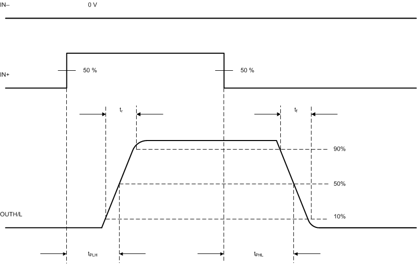 Figure 44. OUTH and OUTL Propagation Delay, Noninverting Configuration
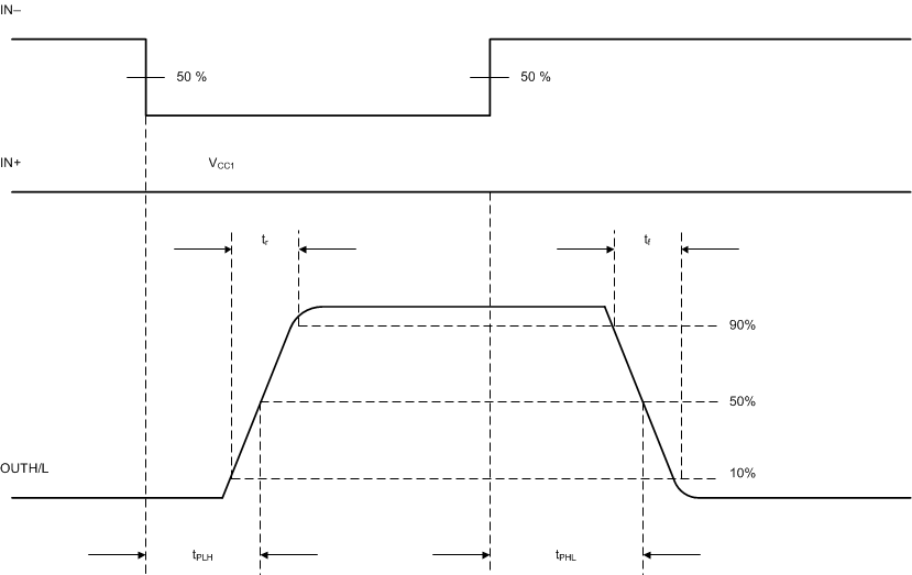 Figure 45. OUTH and OUTL Propagation Delay, Inverting Configuration
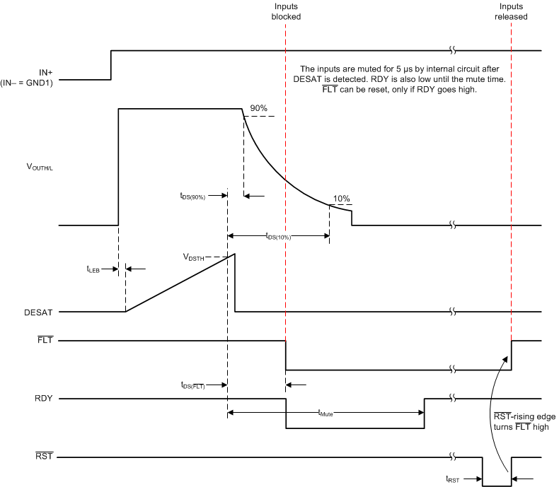 Figure 46. DESAT, OUTH, OUTL, FLT, RST Delay
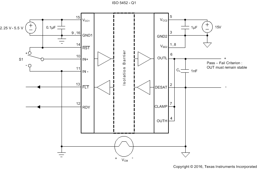 Figure 47. Common-Mode Transient Immunity Test Circuit
9 Detailed Description
9.1 Overview
The ISO5452-Q1 device is an isolated gate driver for IGBTs and MOSFETs. Input CMOS logic and output power stage are separated by a Silicon dioxide (SiO2) capacitive isolation.
The IO circuitry on the input side interfaces with a microcontroller and consists of gate-drive control and RESET (RST) inputs, READY (RDY) and FAULT (FLT) alarm outputs. The power stage consists of power transistors to supply 2.5-A pullup and 5-A pulldown currents to drive the capacitive load of the external power transistors, as well as DESAT detection circuitry to monitor IGBT collector-emitter overvoltage under short-circuit events. The capacitive isolation core consists of transmit circuitry to couple signals across the capacitive isolation barrier, and receive circuitry to convert the resulting low-swing signals into CMOS levels. The ISO5452-Q1 device also has undervoltage lockout circuitry to prevent insufficient gate drive to the external IGBT, and active output pulldown feature which ensures that the gate-driver output is held low, if the output supply voltage is absent. The ISO5452-Q1 device also has an active Miller clamp function which can be used to prevent parasitic turnon of the external power transistor, because of Miller effect, for unipolar supply operation.
9.2 Functional Block Diagram

9.3 Feature Description
9.3.1 Supply and Active Miller Clamp
The ISO5452-Q1 device supports both bipolar and unipolar power supply with active Miller clamp.
For operation with bipolar supplies, the IGBT is turned off with a negative voltage on the gate with respect to the emitter. This prevents the IGBT from unintentionally turning on because of current induced from the collector to the gate because Miller effect. In this condition connecting the CLAMP output of the gate driver to the IGBT gate is not necessary, but connecting the CLAMP output of the gate driver to the IGBT gate is also not an issue. Typical values of VCC2 and VEE2 for bipolar operation are 15 V and –8 V with respect to GND2.
For operation with unipolar supply, typically, VCC2 is connected to 15 V with respect to GND2, and VEE2 is connected to GND2. In this use case, the IGBT can turn on because of additional charge from IGBT Miller capacitance caused by a high-voltage slew-rate transition on the IGBT collector. To prevent IGBT from turning on, the CLAMP pin is connected to IGBT gate and Miller current is sinked through a low-impedance CLAMP transistor.
Miller CLAMP is designed for miller current up to 2 A. When the IGBT is turned off and the gate voltage transitions below 2 V and the CLAMP current output is activated.
9.3.2 Active Output Pull-down
The active output pulldown feature ensures that the IGBT gate OUTH/L is clamped to VEE2 to ensure safe IGBT off-state, when the output side is not connected to the power supply.
9.3.3 Undervoltage Lockout (UVLO) with Ready (RDY) Pin Indication Output
Undervoltage lockout (UVLO) ensures correct switching of IGBT. The IGBT is turned off, if the supply VCC1 drops below VIT-(UVLO1), irrespective of IN+, IN– and RST input until VCC1 goes above VIT+(UVLO1).
In similar manner, the IGBT is turned off if the supply VCC2 drops below VIT-(UVLO2), irrespective of IN+, IN– and RST input till VCC2 goes above VIT+(UVLO2).
The RDY pin indicates status of input and output side UVLO internal protection feature. If either side of device have insufficient supply (VCC1 or VCC2), the RDY pin output goes low; otherwise, RDY pin output is high. The RDY pin also serves as an indication to the micro-controller that the device is ready for operation.
9.3.4 Soft Turn-Off, Fault (FLT) and Reset (RST)
During IGBT overcurrent condition, a mute logic initiates a soft-turn-off procedure which disables OUTH and pulls OUTL to low over a time span of 2 μs. When desaturation is active, a fault signal is sent across the isolation barrier pulling the FLT output at the input side low and blocking the isolator input. Mute logic is activated through the soft-turn-off period. The FLT output condition is latched and can be reset only after RDY goes high, through a low-active pulse at the RST input. RST has an internal filter to reject noise and glitches. By asserting RST for at least the specified minimum duration (800ns), device input logic can be enabled or disabled.
9.3.5 Short Circuit Clamp
Under short-circuit events currents can be induced back into the gate-driver OUTH/L and CLAMP pins because of parasitic Miller capacitance between the IGBT collector and gate terminals. Internal protection diodes on OUTH/L and CLAMP help to sink these currents while clamping the voltages on these pins to values slightly higher than the output side supply.
9.4 Device Functional Modes
For OUTH/L of the ISO5452-Q1 device to follow IN+ in normal functional mode, the RST and RDY pins must be in the high state. Table 1 lists the device functional modes
Table 1. Function Table(1)
| VCC1 | VCC2 | IN+ | IN– | RST | RDY | OUTH/L |
|---|---|---|---|---|---|---|
| PU | PD | X | X | X | Low | Low |
| PD | PU | X | X | X | Low | Low |
| PU | PU | X | X | Low | High | Low |
| PU | Open | X | X | X | Low | Low |
| PU | PU | Low | X | X | High | Low |
| PU | PU | X | High | X | High | Low |
| PU | PU | High | Low | High | High | High |
10 Application and Implementation
NOTE
Information in the following applications sections is not part of the TI component specification, and TI does not warrant its accuracy or completeness. TI’s customers are responsible for determining suitability of components for their purposes. Customers should validate and test their design implementation to confirm system functionality.
10.1 Application Information
The ISO5452-Q1 device is an isolated gate driver for power semiconductor devices such as IGBTs and MOSFETs. The device is intended for use in applications such as motor control, industrial inverters, and switched mode power supplies. In these applications, sophisticated PWM control signals are required to turn the power devices on and off, which at the system level eventually may determine, for example, the speed, position, and torque of the motor or the output voltage, frequency and phase of the inverter. These control signals are usually the outputs of a micro controller, and are at low voltage levels such as 2.5 V, 3.3 V or 5 V. The gate controls required by the MOSFETs and IGBTs, on the other hand, are in the range of 30 V (using unipolar output supply) to 15 V (using bipolar output supply), and require high current capability to be able to drive the large capacitive loads offered by those power transistors. Not only that, the gate drive must be applied with reference to the emitter of the IGBT (Source for MOSFET), and by construction, the emitter node in a gate drive system may swing between 0 to the DC bus voltage, that can be several 100s of volts in magnitude.
The ISO5452-Q1 device is therefore used to level shift the incoming 2.5-V, 3.3-V and 5-V control signals from the microcontroller to the 30 V (using unipolar output supply) to 15 V (using bipolar output supply) drive required by the power transistors while ensuring high-voltage isolation between the driver side and the microcontroller side.
10.2 Typical Applications
Figure 48 shows the typical application of a three-phase inverter using six ISO5452-Q1 isolated gate drivers. Three-phase inverters are used for variable-frequency drives to control the operating speed and torque of AC motors and for high power applications such as high-voltage DC (HVDC) power transmission.
The basic three-phase inverter consists of six power switches, and each switch is driven by one . The switches are driven on and off at high switching frequency with specific patterns that to converter DC bus voltage to three-phase AC voltages.
 Figure 48. Typical Motor Drive Application
10.2.1 Design Requirements
Unlike optocoupler-based gate drivers which require external current drivers and biasing circuitry to provide the input control signals, the input control to the ISO5452-Q1 device is CMOS and can be directly driven by the microcontroller. Other design requirements include decoupling capacitors on the input and output supplies, a pullup resistor on the common drain FLT output signal and RST input signal, and a high-voltage protection diode between the IGBT collector and the DESAT input. Further details are explained in the subsequent sections. Table 2 shows the allowed range for input and output supply voltage, and the typical current output available from the gate-driver.
Table 2. Design Parameters
| PARAMETER | VALUE |
|---|---|
| Input supply voltage | 2.25 V to 5.5 V |
| Unipolar output supply voltage (VCC2 – GND2 = VCC2 – VEE2) | 15 V to 30 V |
| Bipolar output supply voltage (VCC2 – VEE2) | 15 V to 30 V |
| Bipolar output supply voltage (GND2 – VEE2) | 0 V to 15 V |
| Output current | 2.5 A |
10.2.2 Detailed Design Procedure
10.2.2.1 Recommended ISO5452-Q1 Application Circuit
The ISO5452-Q1 has both, inverting and non-inverting gate control inputs, an active low reset input, and an open-drain fault output suitable for wired-OR applications. The recommended application circuit in Figure 49 shows a typical gate driver implementation with unipolar output supply and Figure 50 shows a typical gate driver implementation with bipolar output supply using the ISO5452-Q1 device.
A 0.1-μF bypass capacitor, recommended at input supply pin VCC1 and 1-μF bypass capacitor, recommended at output supply pin VCC2, provide the large transient currents necessary during a switching transition to ensure reliable operation. The 220-pF blanking capacitor disables DESAT detection during the off-to-on transition of the power device. The DESAT diode (DDST) and the 1-kΩ series resistor are external protection components. The RG gate resistor limits the gate charge current and indirectly controls the IGBT collector voltage rise and fall times. The open-drain FLT output and RDY output has a passive 10-kΩ pullup resistor. In this application, the IGBT gate driver is disabled when a fault is detected and will not resume switching until the microcontroller applies a reset signal.
 Figure 49. Unipolar Output Supply
 Figure 50. Bipolar Output Supply
10.2.2.2 FLT and RDY Pin Circuitry
A 50-kΩ pullup resistor is internally connected on the FLT and RDY pins. The FLT and RDY pins are an open-drain output. A 10-kΩ pullup resistor can be used to make it faster rise and to provide logic high when FLT and RDY is inactive, as shown in Figure 51.
Fast common mode transients can inject noise and glitches on FLT and RDY pins because of parasitic coupling. This is dependent on board layout. If required, additional capacitance (100 pF to 300 pF) can be included on the FLT and RDY pins.
 Figure 51. FLT and RDY Pin Circuitry for High CMTI
10.2.2.3 Driving the Control Inputs
The amount of common-mode transient immunity (CMTI) can be curtailed by the capacitive coupling from the high-voltage output circuit to the low-voltage input side of the ISO5452-Q1 device. For maximum CMTI performance, the digital control inputs, IN+ and IN–, must be actively driven by standard CMOS, push-pull drive circuits. This type of low-impedance signal source provides active drive signals that prevent unwanted switching of the ISO5452-Q1 output under extreme common-mode transient conditions. Passive drive circuits, such as open-drain configurations using pullup resistors, must be avoided. A 20-ns glitch filter can filter a glitch up to 20 ns on IN+ or IN–.
10.2.2.4 Local Shutdown and Reset
In applications with local shutdown and reset, the FLT output of each gate driver is polled separately, and the individual reset lines are asserted low independently to reset the motor controller after a fault condition.
 Figure 52. Local Shutdown and Reset for Noninverting (left) and Inverting Input Configuration (right)
10.2.2.5 Global-Shutdown and Reset
When configured for inverting operation, the ISO5452-Q1 device can be configured to shutdown automatically in the event of a fault condition by tying the FLT output to IN+. For high reliability drives, the open drain FLT outputs of multiple ISO5452-Q1 devices can be wired together forming a single, common fault bus for interfacing directly to the micro-controller. When any of the six gate drivers of a three-phase inverter detects a fault, the active low FLT output disables all six gate drivers simultaneously.
 Figure 53. Global Shutdown With Inverting Input Configuration
10.2.2.6 Auto-Reset
In this case, the gate control signal at IN+ is also applied to the RST input to reset the fault latch every switching cycle. Incorrect RST makes output go low. A fault condition, however, the gate driver remains in the latched fault state until the gate control signal changes to the gate low state and resets the fault latch.
If the gate control signal is a continuous PWM signal, the fault latch will always be reset before IN+ goes high again. This configuration protects the IGBT on a cycle by cycle basis and automatically resets before the next on cycle.
 Figure 54. Auto Reset for Noninverting and Inverting Input Configuration
10.2.2.7 DESAT Pin Protection
Switching inductive loads causes large instantaneous forward voltage transients across the freewheeling diodes of IGBTs. These transients result in large negative voltage spikes on the DESAT pin which draw substantial current out of the device. To limit this current below damaging levels, a 100-Ω to 1-kΩ resistor is connected in series with the DESAT diode.
Further protection is possible through an optional Schottky diode, whose low forward voltage assures clamping of the DESAT input to GND2 potential at low voltage levels.
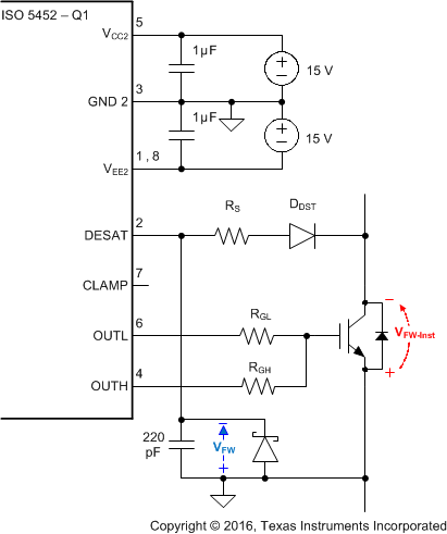 Figure 55. DESAT Pin Protection with Series Resistor and Schottky Diode
10.2.2.8 DESAT Diode and DESAT Threshold
The DESAT function of the diode is used to conduct forward current, allowing sensing of the saturated collector-to-emitter voltage of the IGBT, V(DESAT), (when the IGBT is on) and to block high voltages (when the IGBT is off). During the short transition time when the IGBT is switching, a commonly a high dVCE/dt voltage ramp rate occurs across the IGBT. This results in a charging current ICHARGE = C(D-DESAT) × dVCE/dt, charging the blanking capacitor. C(D-DESAT) is the diode capacitance at DESAT.
To minimize this current and avoid false DESAT triggering, fast switching diodes with low capacitance are recommended. As the diode capacitance builds a voltage divider with the blanking capacitor, large collector voltage transients appear at DESAT attenuated by the ratio of 1+ C(BLANK) / C(D-DESAT).
Because the sum of the DESAT diode forward-voltage and the IGBT collector-emitter voltage make up the voltage at the DESAT-pin, VF + VCE = V(DESAT), the VCE level, which triggers a fault condition, can be modified by adding multiple DESAT diodes in series as shown in Equation 1.
where
- n is the number of DESAT diodes
When using two diodes instead of one, diodes with half the required maximum reverse-voltage rating may be chosen.
10.2.2.9 Determining the Maximum Available, Dynamic Output Power, POD-max
The ISO5452-Q1 maximum allowed total power consumption of PD = 251 mW consists of the total input power, PID, the total output power, POD, and the output power under load, POL:
With:
and:
then:
In comparison to POL, the actual dynamic output power under worst case condition, POL-WC, depends on a variety of parameters:

where
- fINP = signal frequency at the control input IN+
- QG = power device gate charge
- VCC2 = positive output supply with respect to GND2
- VEE2 = negative output supply with respect to GND2
- ron-max = worst case output resistance in the on-state: 4 Ω
- roff-max = worst case output resistance in the off-state: 2.5 Ω
- RG = gate resistor
When RG is determined, Equation 6 is to be used to verify whether POL-WC < POL. Figure 56 shows a simplified output stage model for calculating POL-WC.
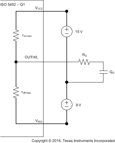 Figure 56. Simplified Output Model for Calculating POL-WC
10.2.2.10 Example
This examples considers an IGBT drive with the following parameters:
Apply the value of the gate resistor RG = 10 Ω.
Then, calculating the worst-case output power consumption as a function of RG, using Equation 6 ron-max = worst case output resistance in the on-state: 4 Ω, roff-max = worst case output resistance in the off-state: 2.5 Ω, RG = gate resistor yields

Because POL-WC = 72.61 mW is less than the calculated maximum of POL = 88.25 mW, the resistor value of RG = 10 Ω is suitable for this application.
10.2.2.11 Higher Output Current Using an External Current Buffer
To increase the IGBT gate drive current, a non-inverting current buffer (such as the npn/pnp buffer shown in Figure 57) may be used. Inverting types are not compatible with the desaturation fault protection circuitry and must be avoided. The MJD44H11/MJD45H11 pair is appropriate for currents up to 8 A, the D44VH10/ D45VH10 pair for up to 15 A maximum.
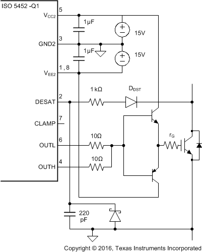 Figure 57. Current Buffer for Increased Drive Current
10.2.3 Application Curves

| CL = 1 nF | RGH = 10 Ω | RGL = 10 Ω |
| VCC2 – GND2 = 15 V | GND2 – VEE2 = 8 V | |
| (VCC2 – VEE2 = 23 V) |

| CL = 1 nF | RGH = 10 Ω | RGL = 10 Ω |
| VCC2 – VEE2 = VCC2 – GND2 = 20 V | ||
11 Power Supply Recommendations
To help ensure reliable operation at all data rates and supply voltages, a 0.1-μF bypass capacitor is recommended at the input supply pin, VCC1, and 1-μF bypass capacitor is recommended at the output supply pin, VCC2. The capacitors should be placed as close to the supply pins as possible. The recommended placement of capacitors is 2-mm (maximum) from input and output power supply pin (VCC1 and VCC2).