SCEA120 October 2022 SN74LXC1T45-Q1 , SN74LXC2T45-Q1 , SN74LXC8T245-Q1 , TXU0101-Q1 , TXU0102-Q1 , TXU0202-Q1 , TXU0304-Q1
1 Application Brief
Fully autonomous vehicles are the holy grail for automobile manufacturers when it comes to Advance Driver Assistance Systems (ADAS), however, today Advance Driver Assistance Systems have not matured enough to offer fully autonomous capabilities. There is no doubt that ADAS systems will eventually mature to support multiple autonomous driving modes. The main automobile sub-systems that will play a key role in enabling autonomous capabilities are the ADAS domain and zone controllers. The ADAS domain controller is responsible for bringing together multiple sensor inputs from cameras, radar, LiDar, proximity sensors, and infrared and combining them with environmental data bases like detailed maps to make decisions about how the automobile should operate under given conditions and then take appropriate actions to notify the driver or even make system decisions to help the driver avoid an accident or keep the automobile moving in a safe manner.
ADAS domain controller sub-systems consist of multiple processors that need to interface with a wide array of sensors and circuits. One design challenge that system designers face when implementing ADAS domain or zone controller designs is overcoming the voltage level mismatch that often arises between the processors and peripheral devices like sensors and sensing sub-systems. New technologies such as software defined ECUs (Electronic Control Units) are expected to result in even more voltage level mismatches as ECUs will need to adapt to a wider range of peripherals.
New processor devices are being developed in smaller CMOS process geometries that require lower-core voltages often <1.2 V which effectively lowers the I/O voltages the processors can support. However, the peripheral devices that domain or zone controllers interface with, often operate at higher I/O voltage levels resulting in I/O voltage mismatches with low voltage processors. The processor to peripheral I/O level mismatch often covers a wide range of voltages and I/O types from push-pull to open-drain interfaces.
One solution that design engineers are turning to is using integrated voltage level translator devices more commonly referred to as level shifter integrated circuits. Level shifters with I/O level shifting support from 1.1 V to 5 V such as TI’s SN74LXC1T45-Q1 (1-channel), SN74LXC2T45-Q1 (2-channel), SN74LXC8T245-Q1 (8-channel), TXU0x04-Q1 (4-channel), TXU0101-Q1 (1-channel), and TXU0102-Q1 (2-channel) families provide ADAS system designers with not only the voltage level translation support they need but also enables robust signal integrity needed for interconnecting ADAS signal chain components. Selecting a voltage level translator with wide voltage range support, typically between 5 V and 1 V, can enable design engineers to resolve voltage level mismatches for many of the data and control signals often found in ADAS domain controller systems. In addition to level translation, TI’s SN74LXC and TXU translation families can also help system designers mitigate the impact of noisy signals. The SN74LXC and TXU families have built-in Schmitt-Trigger inputs that enable ADAS domain or zone controller designers to achieve better noise immunity and cleaner output transitions without the need to add external buffering devices which can introduce unwanted latency that can be detrimental to applications such as ADAS.
Another advantage of using robust level translators is the ability to source additional current drive. Often the latest processors, controllers and FPGAs used in ADAS designs are low voltage devices that have limited I/O drive capability. TI level translators provide additional drive strength often needed to maintain signal integrity in systems with low voltage processors. TI’s LXC family of translators can source up to 32 ma of current drive. Level translation devices like the TXU0304-Q1 can be used to implement level translation for interfaces such as SPI while single channel level translators like SN74LXC1T45-Q1 and TXU0101-Q1 for example, can be used for many different types of GPIO translation needs.
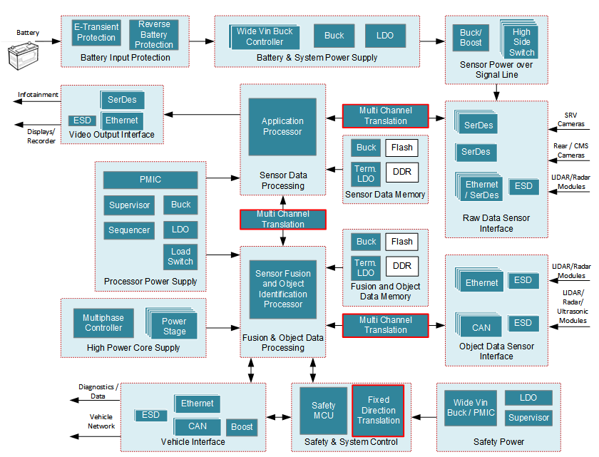
See Figure 1-1 for common places where level translation may be needed within an ADAS domain controller design. See Table 1-1 for level translation suggestions based on common interfaces. For more information on level translation solutions from Texas Instruments, please visit TI’s level translation landing page.
 Figure 1-1 ADAS Domain Controller Reference Diagram and Common Level Translation Use Cases
| Interface | TI Recommended Device | |
|---|---|---|
| 3.6 V maximum | 5.5 V maximum | |
| FET Replacement | 2N7001T-Q1 | SN74LXC1T45-Q1 / TXU0101-Q1 |
| 1-Bit GPIO/Clock Signal | SN74AXC1T45-Q1 | SN74LXC1T45-Q1 / TXU0101-Q1 |
| 2-Bit GPIO | SN74AXC2T245-Q1 | SN74LXC2T45-Q1 / TXU0102-Q1/TXU0202-Q1 |
| 2-Pin JTAG/UART | SN74AXC2T45-Q1 | SN74LXC2T45-Q1 / TXU0102-Q1/TXU0202-Q1 |
| I2C/MDIO/SMBus | TXS0102-Q1 / LSF0102-Q1 | TXS0102-Q1 / LSF0102-Q1 |
| 4-Bit GPIO | SN74AXC4T245-Q1 | TXB0104-Q1 / TXU0104-Q1 |
| UART | SN74AXC4T245-Q1 | TXB0104-Q1 / TXU0204-Q1 |
| SPI | SN74AXC4T774-Q1 / TXB0104-Q1 | TXB0104-Q1 / TXU0304-Q1 |
| JTAG | SN74AXC4T774-Q1 / TXB0104-Q1 | TXB0104-Q1 / TXU0204-Q1 |
| I2S/PCM | SN74AXC4T774-Q1 / TXB0104-Q1 | TXB0104-Q1 / TXU0204-Q1 |
| Quad-SPI | TXB0106-Q1 | TXB0106-Q1 |
| SDIO/SD/MMC | TXS0206 or TWL1200 | N/A |
| 8 Bit GPIO/RGMII | SN74AXC8T245-Q1 | SN74LXC8T245-Q1 |