SBOA532 November 2021 INA901-SP
Design Goals
| Input | Output | Supply | Common-Mode Voltage | Error | Total Ionizing Dose | Single-Event Immunity | ||
|---|---|---|---|---|---|---|---|---|
| ILOAD,MIN | ILOAD,MAX | VOUT, min | VOUT, max | VS | VCM | Output Error | TID | SEL |
| –7.5 A | 7.5 A | 500 mV | 3.5 V | 5 V | 24 V | < 2% | 50 krad (Si) | 75 MeV × cm2/mg |
Design Description
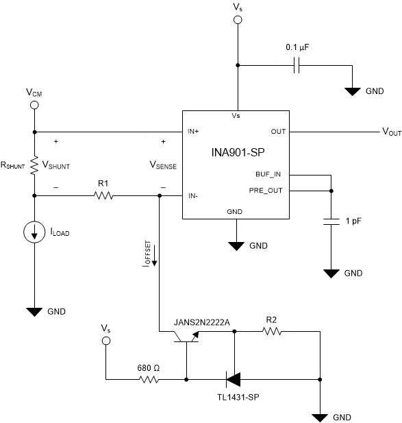
This circuit that utilizes a TL1431-SP, JANS2N2222A NPN transistor (see the following image), and passive components to achieve bidirectional sensing from a unidirectional current sense amplifier, the INA901-SP. In this particular setup, the normal operating load is from –7.5 A to 7.5 A, with a supply voltage of 5 V. This topology may be used any supply voltage independent of the desired offset. In addition to this functionality, this circuit implements the INA901-SP, which is a Radiation-Hardness-Assured (RHA), 50-krad (Si) capable device at Low Dose Rate, that is also Single Event Latch-up (SEL) Immune to 75 MeV-cm2/mg at 125°C. The solution presented in this circuit is a high-side implementation, with a common-mode voltage range of 2.5 V to 65 V.
Design Notes
- This topology is meant for high-side implementation, where the IN+ and IN– pin of the INA901-SP are referenced to VCM of the application. While this circuit is capable of withstanding the full 65 V common mode of the INA901-SP, a limitation exists on the lower end, and VCM must be held > 2.5 V. This is due to reference of the TL1431-SP of 2.5 V, and the need for the current flow to sink towards the TL1431-SP for proper offset voltage creation. Therefore, the common-mode voltage of the IN– pin must be > 2.5 V to ensure valid operation.
- For the presented design, a 24 VCM is considered, and the JANS2N2222A is chosen to complete the design based on these parameters. A BJT possessing greater VCE capabilities is needed for high-voltage applications > 50 VCM.
- Care should be taken when designing with the INA901-SP to ensure the full-scale input range of the device remains above 20 mV for best performance. If VSENSE is allowed below 20 mV, the device may produce additional errors inside of this operating condition. See the INA901-SP Radiation Hardened, –15-V to 65-V Common Mode, Unidirectional Current-Shunt Monitor data sheet for more information.
- While this circuit provides the ability to measure in multiple directions, it does not change the fact that the INA901-SP is inherently a unidirectional device. This infers that one direction of current sensing will be more accurate than the other, as one direction will measure towards the offset voltage of the device, leading to increased error in this direction. The effects of this may be mitigated in part by the use of a one-point calibration, and is discussed later in this document.
Design Steps
- Design the Offset Current: The offset current ultimately flows over R1 to create the RTI offset sense voltage, but is determined by resistor R2. Because the default reference voltage of the TL1431-SP is 2.5 V, a 1-kΩ resistor is chosen, and the offset current is calculated as shown in the following equation:
- Design RTI Offset Voltage Point: With IOFFSET determined in the previous equation, R1 may now be selected to determine the VREF point of the design. For the given design, a desired VREF of 2 V was chosen, but resistor selection ultimately led to a 1.96-V design. This point is determined by the following equations:
- Choose RSHUNT to Optimize Input Range: With the RTI Offset designed, a shunt may now be chosen for the desired sensing range. For the INA901-SP, maintain the lower sensing bound at > 20 mV for optimal performance, this shows that the amount of sensing headroom from VREF is calculated as in the following equation:
From the desired –7.5-A design target, it is calculated that the maximum allowable shunt to achieve this goal is found using the following:
As the design ILOAD target in the remaining direction is symmetric about VREF, 10 mΩ was selected to complete the design. The final input VSENSE swing is calculated as:
The expected corresponding output is found using:
- Verify shunt derating is
sufficient: A necessary aspect of proper shunt design is ensuring that
the design choice has sufficient margin for power derating. As the device heats
in the environment, the amount of power the shunt is capable of dissipating is
derated by a certain factor. For continuous sensing, this factor can be as high
as 0.6. Taking this into account, for the design, a shunt must be chosen that is
rated for at least the following:
So for a successful design, a shunt of at least 1-W rated power is chosen for continuous sensing.
- Choose the correct BJT NPN transistor: Dependent on the common modes expected to be seen by the application, a corresponding BJT must be chosen to be able to withstand this VCM. The voltage ultimately seen by the BJT is calculated as in the following equation:
Add some margin for any potential voltage transients on the common mode. For the given design, the JANS2N2222A is chosen, as it is able to withstand a VCE of 50 V maximum, and meets the needs of the design. The expected power dissipated through the BJT is found with the following equation:
- Examine Error. Calibrate if necessary: As discussed in previous sections, it is expected that the current sense amplifier will be more accurate in the direction of measurement as the output is driven toward supply. Less accurate measurements are expected as the sense voltage decreases, and errors from the offset voltage begin to have more effect. A remedy for this is to perform a one-point calibration in logic to reduce the effects of the offset voltage.
A one-point calibration is performed by applying the condition, to the system, capturing the actual value output by the INA901-SP, and maintaining the difference between this value and the calculated ideal in memory. The output of the device is then consistently shifted by this amount. An example of the effects of this are shown in the following simulated results.
Design Simulations
DC Sweep Results, –7.5 A < ILOAD < 7.5 A
 INA901-SP High-Side Bidirectional Circuit Performance Over Load
 Error Curves, Pre- and Post-Calibration From Simulation Data
Calibration of the raw data from simulation results in the VSENSE = 0 point shifting to an error of 0%, and a < 1% error over the full load range, thus meeting the design goal. Note that parameters such as device offset and input bias currents in TINA-TI models reflect typical data sheet parameters, and additional error may be exhibited pre- and post-calibration due to variation in these parameters. For more information, see the Bidirectional Topologies for the INA901-SP application note.
Design References
See the TI Precision Labs, Current Sense Amplifiers video series.
| INA901-SP | |
|---|---|
| VS | 2.7 V to 16 V |
| VCM | –15 V to 65 V |
| VOUT | GND+3 mV to VS – 50 mV, typical |
| VOS | ±500 μV, typical |
| Iq | 350 μA, typical |
| IB | ±8 μA, typical |
TID Characterization (ELDRS-Free) |
50 krad (Si) |
SEL Immune to LET |
75 MeV-cm2/mg |
| INA901-SP | |