SBOA516 May 2021 LMH32404-Q1
1 Application Brief
Introduction
As many modern LiDAR systems are moving towards solid state configurations with multi-channel sensor arrays, system density for the amplification and data-processing portion of the signal chain becomes challenging. For systems with many optical input channels, it is impractical to have single transimpedance amplifiers connected to each diode output and often requires additional multiplexers or other switching solutions to connect to the digitizer, which can introduce further complexity and signal degradation.
To solve the problems of high-density multi-channel optical front-end design, Texas Instruments has released the LMH32404-Q1. The LMH32404-Q1 is an automotive Q100 qualified four channel, differential output, multiplexed transimpedance amplifier with integrated clamping and ambient light cancellation. The multiple channels, integrated multiplexing, and other features make the LMH32404-Q1 an excellent choice of amplifier to alleviate the issues surrounding multiple-channel optical systems.
How the LMH32404-Q1 Improves
Multi-channel Optical Designs
Traditional optical front-end configurations do not often work well with high density photodiode arrays because of the channel density and number of number of amplifiers required between the optical array and ADC. The LMH32404-Q1 features four transimpedance amplifier channels with 20 kΩ of gain and can be multiplexed into a single set of differential outputs.
Figure 1-1 shows a comparison of a non-integrated front end using individual amplifiers, a multiplexer, and fully-differential amplifier (FDA) to connect to the differential input ADC. In comparison, the front end using the LMH32404-Q1 is able to connect four channels per amplifier to each ADC or set of ADC differential inputs.

Figure 1-1 Solution Size Comparison

Figure 1-2 LMH32404 Multiplexing
Configuration Examples
For further system flexibility, The LMH32404-Q1 allows the user to configure the output multiplexing in multiple ways with independent output switch control. Figure 1-2 shows two common configurations. In a four-to-four configuration the LMH32404-Q1 operates with no output multiplexing with each input and corresponding differential output active. This configuration is useful when the user needs to be able to capture data from four optical sensors simultaneously. In a four-to-one configuration the LMH32404-Q1 internally multiplexes all four differential outputs into a single differential output, which significantly increases channel density for systems that do not need to record all inputs simultaneously. However, the LMH32404-Q1 is not just limited to one-to-one or four-to-one configurations. The outputs can be configured in any other permutation such as one channel operating in one-to-one mode with the other three channels multiplexed in a three-to-one configuration.
 Figure 1-3 LMH32404 Simplified Internal
 Block Diagram
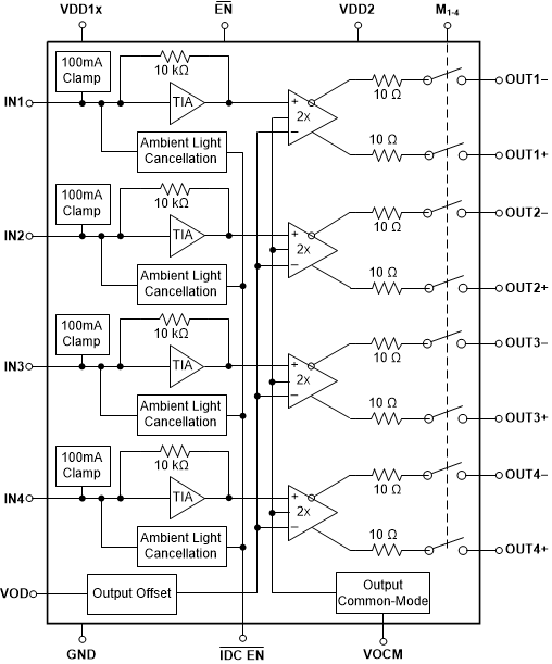
Figure 1-3 shows the basic block diagram of the LMH32404-Q1 with the four channels featuring the additional features of clamps, ambient light cancellation, and differential outputs. The multiplexing is achieved by connected the corresponding positive and negative outputs on the PCB. The input current clamps help to protect the amplifier inputs when presented with unexpectedly large input currents, which often happen in optical systems that are used in highly variable environments. The optional DC current cancellation circuit can be used to cancel DC current caused by ambient light incident on the photodiodes that otherwise can cause additional offset and error in the system. The output common mode control (VOCM) allows the user to easily set the common mode of the differential outputs to match the common mode of an ADC. For unipolar current sources such as photodiodes, the output differential offset pin (VOD) allows the user to set a baseline differential output when no input signal is present in order to maximize the differential output dynamic range. For more details on the maximizing output dynamic range, refer to Maximizing the dynamic range of analog front ends having a transimpedance amplifier.
Measurements using LMH32404-Q1
and ADC12QJ1600
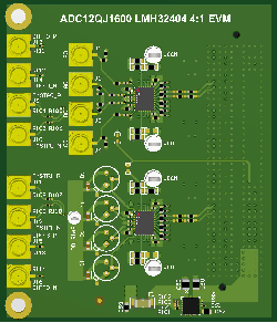
The LMH32404-Q1 performance was measured in conjunction with the ADC12QJ1600-Q1 analog to digital converter to demonstrate a typical application circuit. Figure 1-4 shows the interface board designed to connect the LMH32404-Q1 in a 4:1 multiplexed output configuration to one of the input of the ADC12QJ1600-Q1. The board features two LMH32404-Q1 devices, one configured for electrical inputs and the other for a photodiode input.
 Figure 1-4 LMH32404-Q1 Interface Board for
ADC12QJ1600-Q1
Figure 1-4 LMH32404-Q1 Interface Board for
ADC12QJ1600-Q1Figure 1-5 and Figure 1-6 show the data measured from the ADC12QJ1600-Q1 using a 10ns and 5ns duration electrical input pulse on a single channel of the LMH32404-Q1. These pulses are similar to outputs seen in a typical LiDAR application.
 Figure 1-5 10 ns Pulse Electrical Input
 Figure 1-6 5 ns Pulse Electrical Input
Figure 1-7 shows the data from the ADC12QJ1600-Q1 when the LMH32404-Q1 inputs switch between different input channels with electrical inputs. The initial output shows a 10ns duration pulse train on channel 1 followed by a 20 MHz sinusoidal signal on channel 2 and then the output with all channels turned off but the input signals still present. The sinusoidal signal amplitude is less than full scale because the VOD pin was set to center the full scale signal for the unipolar pulse input. The channels were switched at approximately 0.6 μs intervals with 25 ns spacing between channel activation.
 Figure 1-7 Multiplexed Channel Switching
Figure 1-8 shows the ADC12QJ1600-Q1 data with the LMH32404-Q1 driven by a photodiode with a modulated optical signal input. The ringing from the varying amplitude of the sinusoidal input was a result of variance in the lithium niobate (LiNbO3) optical intensity modulator's drift and stability.
 Figure 1-8 50 MHz Optical Sine Wave Input
The LMH32404-Q1 Maximizes System Flexibility
With all of the combined features and flexibility of the LMH32404-Q1, it makes an excellent choice to improve system designs. The multi-channel, user-configurable, differential output multiplexing creates an extremely flexible platform to meet system density and integration requirements, while reducing the need for additional components. For more information refer to the LMH32404-Q1 product page and data sheet.