SBOA230 June 2021 OPA325 , TLV316 , TLV9062
| Input | Output | Supply | |||
|---|---|---|---|---|---|
| ViMin | ViMax | VoMin | VoMax | Vcc | Vee |
| –2.45V | +2.45V | 0.05V | 4.95V | 5V | 0V |
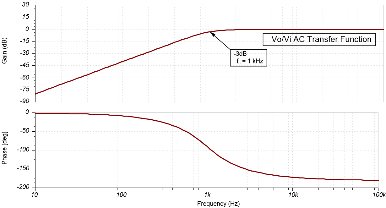
| Gain | Cutoff Frequency (fc) | Max Frequency (fmax) | Vref |
|---|---|---|---|
| –1V/V | 1kHz | 10kHz | 2.5V |
Design Description
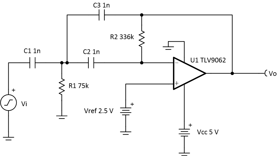
The multiple-feedback (MFB) high-pass (HP) filter is a 2nd-order active filter. Vref provides a DC offset to accommodate for single-supply applications. This HP filter inverts the signal (Gain = –1V/V) for frequencies in the pass band. An MFB filter is preferable when the gain is high or when the Q-factor is large (for example, 3 or greater).
Design Notes
- Select an op amp with sufficient input common-mode range and output voltage swing.
- Add Vref to bias the input signal to meet the input common-mode range and output voltage swing.
- Select the capacitor values first since standard capacitor values are more coarsely subdivided than the resistor values. Use high-precision, low-drift capacitor values to avoid errors in fc.
- To minimize the amount of slew-induced distortion, select an op amp with sufficient slew rate (SR).
- For HP filters, the maximum frequency is set by the gain bandwidth (GBW) of the op amp. Therefore, be sure to select an op amp with sufficient GBW.
Design Steps
The first step in design is to find component values for the normalized cutoff frequency of 1 radian/second. In the second step, the cutoff frequency is scaled to the desired cutoff frequency with scaled component values.
The transfer function for a 2nd-order MFB high pass filter is given by:
- Set normalized values of
C1, C2, and C3 (C1n,
C2n, and C3n) and calculate normalized values of
R1 and R2 (R1n and R2n) by
setting wc to 1radian/sec (or fc = 1 / (2 × π)Hz). For a
2nd-order Butterworth filter, (see the Butterworth Filter Table in the
Active Low-Pass Filter Design Application Report).
- Scale the component values and
cutoff frequency. The resistor values are very small and capacitors values are
unrealistic, hence these have to be scaled. The cutoff frequency is scaled from
1 radian/sec to w0. If we assume m to be the scaling factor,
increase the resistors by m times, then the capacitor values have to
decrease by 1/m times to keep the same cutoff frequency of 1 radian/sec.
If we scale the cutoff frequency to be w0 then the capacitor values
have to be decreased by 1/w0. The component values for the design
goals are calculated in step 3 and 4.
- Set
C1, C2, and C3 to 1nF and calculate m.
- Calculate R1 and
R2 based on m.
- Calculate minimum required GBW and
SR for fmax. Be sure to use the noise gain for GBW calculations. Do
not use the signal gain of –1V/V.
The TLV9062 device has GBW of 10MHz and SR of 6.5V/µs, so the requirements are met.
Design Simulations
AC Simulation Results
Transient Simulation Results
.") Filter Output in Response to a 5-Vpp, 10-kHz Input-Signal (Gain =
–1V/V).
Filter Output in Response to a 5-Vpp, 10-kHz Input-Signal (Gain =
–1V/V).") Filter Output in Response to a 5-Vpp, 100-Hz Input-Signal (Gain =
–0.01V/V)
Filter Output in Response to a 5-Vpp, 100-Hz Input-Signal (Gain =
–0.01V/V)Design References
- See Analog Engineer's Circuit Cookbooks for TI's comprehensive circuit library.
- SPICE Simulation File: SBOC599.
- TI Precision Labs.
- Active Low-Pass Filter Design Application Report
Design Featured Op Amp
| TLV9062 | |
|---|---|
| Vss | 1.8V to 5.5V |
| VinCM | Rail-to-Rail |
| Vout | Rail-to-Rail |
| Vos | 0.3mV |
| Iq | 538µA |
| Ib | 0.5pA |
| UGBW | 10MHz |
| SR | 6.5V/µs |
| #Channels | 1, 2, 4 |
| www.ti.com/product/TLV9062 | |
Design Alternate Op Amp
| TLV316 | OPA325 | |
|---|---|---|
| Vss | 1.8V to 5.5V | 2.2V to 5.5V |
| VinCM | Rail-to-Rail | Rail-to-Rail |
| Vout | Rail-to-Rail | Rail-to-Rail |
| Vos | 0.75mV | 0.150mV |
| Iq | 400µA | 650µA |
| Ib | 10pA | 0.2pA |
| UGBW | 10MHz | 10MHz |
| SR | 6V/µs | 5V/µs |
| #Channels | 1, 2, 4 | 1, 2, 4 |
| www.ti.com/product/TLV316 | www.ti.com/product/OPA325 |