SBOA226 June 2021 OPA325 , TLV316 , TLV9062
| Input | Output | Supply | |||
|---|---|---|---|---|---|
| ViMin | ViMax | VoMin | VoMax | Vcc | Vee |
| –2.45V | +2.45V | 0.05V | 4.95V | 5V | 0V |
| Gain | Cutoff Frequency (fc) | Vref |
|---|---|---|
| 1V/V | 10kHz | 2.5V |
Design Description
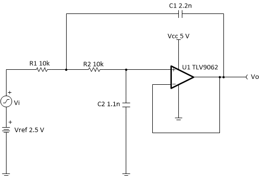
The Butterworth Sallen-Key low-pass filter is a second-order active filter. Vref provides a DC offset to accommodate for single-supply applications. A Sallen-Key filter is usually preferred when small Q factor is desired, noise rejection is prioritized, and when a non-inverting gain of the filter stage is required. The Butterworth topology provides a maximally flat gain in the pass band.
Design Notes
- Select an op amp with sufficient input common-mode range and output voltage swing.
- Add Vref to bias the input signal to meet the input common-mode range and output voltage swing.
- Select the capacitor values first since standard capacitor values are more coarsely subdivided than the resistor values. Use high-precision, low-drift capacitor values to avoid errors in fc.
- To minimize the amount of slew-induced distortion, select an op amp with sufficient slew rate (SR).
Design Steps
The first step is to find component values for the normalized cutoff frequency of 1 radian/second. In the second step the cutoff frequency is scaled to the desired cutoff frequency with scaled component values.
The transfer function for second order Sallen-Key low-pass filter is given by:
Here,
- Set normalized values of
R1 and R2 (R1n and R2n) and
calculate normalized values of C1 and C2
(C1n and C2n) by setting wc to 1
radian/sec (or fc = 1 / (2 × π) Hz). For the second-order
Butterworth filter, (see the Butterworth Filter Table in the Active Low-Pass Filter Design Application Report).
- Scale the component values and
cutoff frequency. The resistor values are very small and capacitors values
are unrealistic, hence these have to be scaled. The cutoff frequency is
scaled from 1 radian/sec to w0. If m is assumed to be the
scaling factor, increase the resistors by m times, then the capacitor
values have to decrease by 1/m times to keep the same cutoff
frequency of 1 radian/sec. If the cutoff frequency is scaled to be
w0, then the capacitor values have to be decreased by 1 /
wo. The component values for the design goals are calculated
in steps 3 and 4. Equation 1.Equation 2.Equation 3.
- Set R1 and R2
values:Equation 4.Equation 5.
- Calculate C1 and C2 based on m and
w0.
- Calculate the minimum required
GBW and SR for fc.
The TLV9062 device has a GBW of 10MHz and SR of 6.5V/µs, so the requirements are met.
Design Simulations
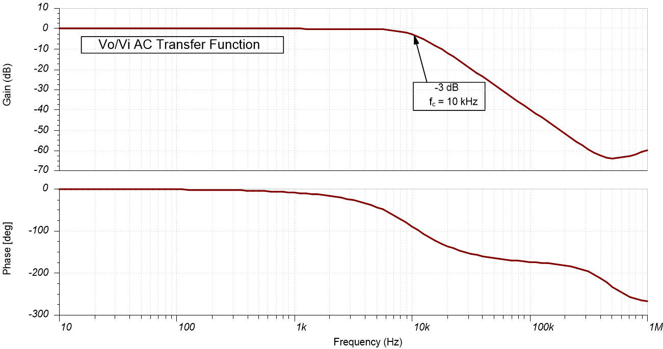
AC Simulation Results
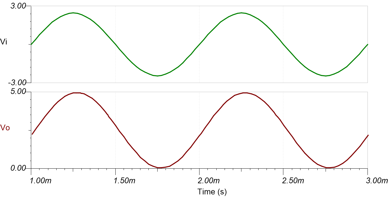
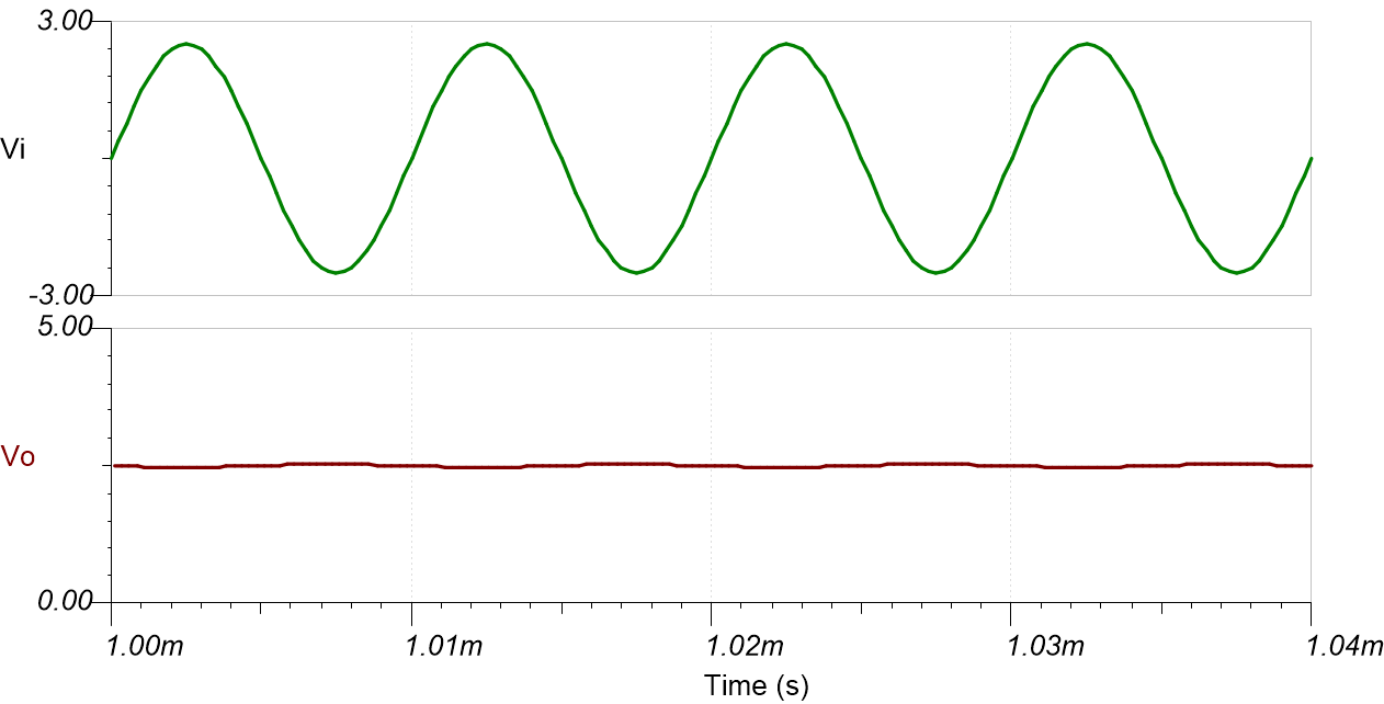
Transient Simulation Results
The following image shows the filter output in response to 5-Vpp, 1-kHz input signal (gain = 1V / V).
The following image shows the filter output in response to 5-Vpp, 100-kHz input signal (gain = 0.01 V/V).
Design References
- See Analog Engineer's Circuit Cookbooks for TI's comprehensive circuit library.
- SPICE Simulation File SBOC598.
- TI Precision Labs.
- Active Low-Pass Filter Design Application Report
Design Featured Op Amp
| TLV9062 | |
|---|---|
| Vss | 1.8V to 5.5V |
| VinCM | Rail-to-Rail |
| Vout | Rail-to-Rail |
| Vos | 0.3mV |
| Iq | 538µA |
| Ib | 0.5pA |
| UGBW | 10MHz |
| SR | 6.5V/µs |
| #Channels | 1, 2, 4 |
| www.ti.com/product/TLV9062 | |
Design Alternate Op Amp
| TLV316 | OPA325 | |
|---|---|---|
| Vss | 1.8V to 5.5V | 2.2V to 5.5V |
| VinCM | Rail-to-Rail | Rail-to-Rail |
| Vout | Rail-to-Rail | Rail-to-Rail |
| Vos | 0.75mV | 0.150mV |
| Iq | 400µA | 650µA |
| Ib | 10pA | 0.2pA |
| UGBW | 10MHz | 10MHz |
| SR | 6V/µs | 5V/µs |
| #Channels | 1, 2, 4 | 1, 2, 4 |
| www.ti.com/product/TLV316 | www.ti.com/product/OPA325 |