SBAA550 May 2022 ADC128S102-SEP , INA240-SEP , OPA4H014-SEP
1 Application Brief
Design Description
This document demonstrates two current-sensing circuits using ADC128S102-SEP, INA240-SEP, TPS73801-SEP, and OPA4H014-SEP. TPS73801-SEP is a radiation-tolerant, low-dropout regulator (LDO) used for creating a 5-V reference voltage for the circuit. ADC128S102-SEP is a radiation-tolerant, low-power, eight-channel,
50-kSPS to 1-MSPS, 12-bit analog-to-digital converter (ADC). This product is similar to the ADC128S102QML-SP, which is a radiation-hardened version of this ADC that has been in the market since 2008. In comparison, the ADC128S102-SEP has lower radiation performance with TID = 30 krad (Si), but is a lower cost, smaller size SAR ADC designed for low-Earth orbit (LEO) applications.
In the first circuit, ADC128S102-SEP is directly driven by INA240-SEP, which is a current-sensing amplifier with a fix gain of 20 V/V and accepts a common-mode input voltage from –4 V to 80 V. In the second circuit, ADC128S102-SEP is driven by OPA4H014-SEP for additional bandwidth and gain. Both circuits use fully radiation-tolerant ICs with TID level equal or greater than 30 krad(Si). Both circuits are simulated achieving the same accuracy and the maximum sampling rates are compared.
Circuit 1 Schematic
The following circuit is designed to sense current from 0 A to 20 A. INA240-SEP has a very wide range of common-mode input voltage from –4 V to 80 V, and it can be used for applications such as motor control, satellite solar panel current sensing, and so forth. The INA240-SEP helps reducing circuit size and cost by simplifying the analog front-end circuit.
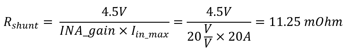
The Y14870R1152B9W device (shown in the following image) is a shunt resistor (Rshunt) with a customized resistance value of 11.25 mΩ.
 Current Sensing Circuit 1 Schematic
Circuit 1 Design Steps
The following steps show how to find resistors and capacitors values in the circuit 1 schematic to map the INA240-SEP output to a range of 0 V to 4.5 V and to maximize the ADC sampling rate
- Tie REF1 and REF2 to ground. Determine the maximum input current (Iin_max) and the current sense amplifier gain (INA_gain). From the INA240-SEP Wide Common-Mode Range, High- and Low-Side, Bidirectional, Zero-Drift, Current-Sense Amplifier in Space Enhanced Plastic data sheet, INA240-SEP has a gain of 20 V/V. Calculate shunt resistor (Rshunt) value to map the output to a range of 0 V to 4.5 V. Equations are provided as follows:
- Set C2 to 680 pF and R1 to 30 Ω. C2 is about 20 times larger than sample and hold capacitor (Csh), which is 33 pF, resulting in a value of 660 pF. R1 is normally in a range of 10 Ω to 200 Ω, and is optimized by sweeping for the smallest sampled signal settling time in Csh. In this case, R1 resulted to be 30 Ω.
- Simulate in TINA TI-SPICE with the lowest sampling rate of 50 kSPS. To achieve 50 kSPS sampling rate, the digital clock input (sclk) is 800 MHz. Conversion time (tconv) is 13 clock cycles, which is 16.25 μs. Similarly, acquisition time (tacq) is 3.75 μs. This ensures enough time for the sampled signal to settle within the acquisition time.
- Measure the shortest sampled signal settling time from simulation. Using this settling time, calculate the maximum ADC sampling rate where the analog front end can settle adequately using the following equation:

- Recalculate tacq and tconv with the fastest sampling rate calculated in step 4, then simulate again in TINA TI-SPICE to confirm the sampled signal indeed settled within the acquisition time (tacq).
Circuit 1 Simulation Result
Following the Circuit 1 Design Steps instructions, the shunt resistor is calculated to be 11.25 mΩ. Both REF1 and REF2 are tied to ground. R1 and C2 are 30 Ω and 680 pF.
 Circuit 1 Schematic in TINA TI-Spice
 Circuit 1 Simulation Result in TINA TI-Spice
The sampling rate is optimized for a maximum sampling rate, which is 72 kSPS with a clock frequency of 1.15 MHz. Simulation shows a 544 μV out of 5-V error at Csh, which is less than half of the LSB.
Circuit 2 Schematic
The following current-sensing circuit is designed to sense current from –5 A to 5 A. Compared to circuit 1, circuit 2 has a second amplification stage for additional gain and bandwidth. The following list shows two benefits.
- INA240-SEP comes with a fixed gain of 20. To obtain a full range of output, the shunt resistor value might need to be customized. Hence, it is more flexible to design with an adjustable second gain stage.
- ADC128S102-SEP has a sampling rate of 1 MSPS. However, the INA240-SEP could only drive it up to 72 kSPS. If a higher sampling rate is required, the 11-MHz high-precision op-amp, OPA4H014-SEP, is a good driver option.
 Current Sensing Circuit 2 Schematic
Circuit 2 Design Steps
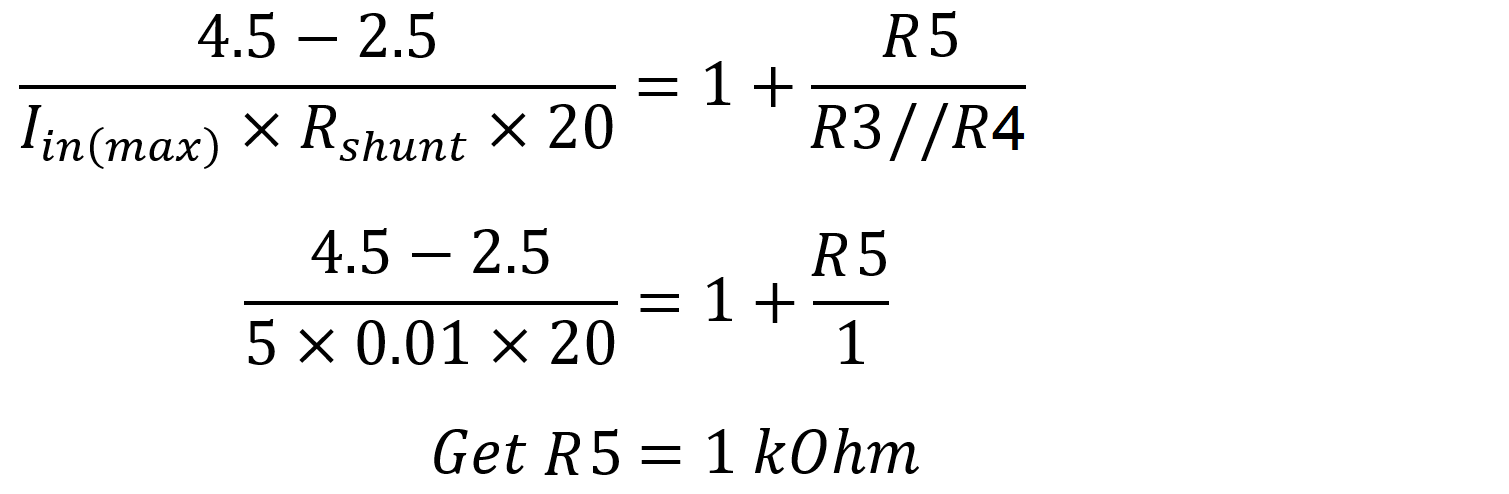
- Tie REF1 to ground and REF2 to 5 V, "VA +5V" pin, to bias the output at 2.5 V
- Select a common shunt resistor (Rshunt) value such that INA240-SEP the output voltage is between 0 V and 4.5 V. In this case, a 10 mΩ, Rshunt is chosen, resulting in INA240-SEP outputs voltage from 1.5 V to 3.5 V
- Set the second amplification stage gain. If R3 and R4 are both set to 2 kΩ, R5 can be calculated using the following formulas:
- Navigate to ADC SAR Drive in the Analog Engineer’s Calculator and calculate C3 (Cfilt) and R6 (Rfilt). An example of a calculation result follows. Since the acquisition time (tacq) is unknown, tune the value until the resulting gain bandwidth is below the gain bandwidth product (GBW) of OPA4H014-SEP, which is 11 MHz.
 C3 and R6 Calculation in Analog Engineer’s Calculator
 - Simulate in TINA-TI SPICE to measure the sampled signal settling time to confirm it indeed settled within the acquisition time (tacq)
Circuit 2 Simulation Result
Following the Circuit 2 Design Steps, the shunt resistor is chosen to be a common value, 10 mΩ. With the op-amp gain set to 2, the ADC input signal ranges from 0.5 V to 4.5 V. C3 is 680 pF, and R6 is optimized by sweeping and found to be 35 Ω for smallest ADC input signal settling time.
 Circuit 2 Schematic in TINA TI-Spice
 Circuit 2 Simulation Result in TINA TI-Spice
The maximum sampling rate is found to be 568 kSPS with a clock frequency of 9.09 MHz. Simulation shows a 545 μV out of 5-V error at Csh, which is less than half of the LSB.
Error Analysis
The following equations are for calculating error introduced by the ADC analog front end (AFE):
Gain error caused by shunt resistor tolerance (Rshunt) and temperature drift:
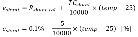
- eshunt: the gain error causing by the shunt resistor [%]
- Rshunt_tol: tolerance of Rshunt [%]
- TCshunt: temperature coefficient of Rshunt [ppm/℃]
- temp: temperature [℃]
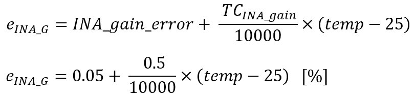
Gain error caused by INA240-SEP:
where
- eINA_G: gain error caused by INA240-SEP [%]
- INA_gain_error: INA gain error from the data sheet [%]
- TCINA_gain: INA gain error temperature coefficient from the data sheet [ppm/℃]
Offset error caused by INA240-SEP:
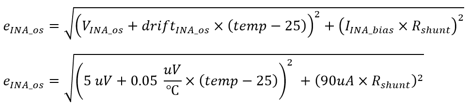
- eINA_os: offset error caused by INA240-SEP [μV]
- VINA_os: offset voltage from INA240-SEP data sheet [μV]
- driftINA_os: offset drift from INA240-SEP data sheet [μV/℃]
- IINA_bias: bias current from INA240-SEP data sheet [μA]
- Rshunt: shunt resistor value [Ω]
Noise at INA240-SEP output:
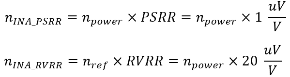
where
- nINA_PSRR: noise from power supply affection on INA240-SEP output [μV]
- PSRR: power rejection ratio from INA240-SEP data sheet [μV/V]
- npower: noise from power supply [μV]
- nINA_RVRR: noise from reference voltage affection on INA240-SEP output [μV]
- nref: reference voltage noise [μV]
- RVRR: reference voltage reflection ratio from INA240-SEP data sheet [μV/V]
Nonlinearity Error (INL) of INA240-SEP is found to be 0.01% in the data sheet.
Gain error from OPA4H014-SEP (only apply to circuit 2):
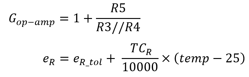
where
- Gop-amp: gain of the op-amp circuit [V/V]
- eR: resistors (including R3, R4, and R5) errors [%]
- eR_tol: resistors (including R3, R4, and R5) tolerance [%]
- TCR: resistor (including R3, R4, and R5) temperature coefficient [ppm/℃]
Offset error from OPA4H014-SEP (only apply to circuit 2):

where
- eOPA_os: offset error from OPA4H014-SEP [%]
- e5Vref: 5-V reference voltage error [%]
- VOPA_os: op-amp offset voltage from OPA4H014-SEP data sheet [μV]
- driftOPA: op-amp offset drift from OPA4H014-SEP data sheet [μV/℃]
- IOPA_bias: op-amp bias current from OPA4H014-SEP data sheet [nA]
Error introduced by ADC128S102-SEP and TPS73801-SEP, which is used to provide the 5-V reference voltage to pin VA of ADC128S102-SEP, could be calculated using the TUE Calculator in Analog Engineer's Calculator. To use the Total Unadjusted Error (TUE) calculator, input the values listed in the screen from the device data sheet:
 TUE Calculation, Displaying ADC Specifications and Non-calibrated
Results
TUE Calculation, Displaying ADC Specifications and Non-calibrated
Results
 TUE Calculation, Displaying LDO Specifications and Calibrated Results
The TUE calculator was used to solve for the Total Unadjusted Error of the system. TUE Calculation, Displaying ADC Specifications and Non-calibrated Results displays the ADC error tab with the values input from the ADC128S102-SEP data sheet. TUE Calculation, Displaying LDO Specifications and Calibrated Results displays the Reference Error tab with the values input from the TPS73801-SEP data sheet. Fill in both of these tabs for an accurate TUE result. Note that the amplifier Error tab is not used in this example. The Analog Engineer's Calculator provides results using various calibration options, under Analysis Options.
The previous two images display the non-calibrated results and the results with Gain and Offset calibrated, respectively. With temperature ranges from –55°C to 125°C, calculations show that ADC128S102-SEP and TPS73801-SEP contribute around 1.35% typical error and 2.68% maximum error without calibration, and 0.1636% typical error and 0.1660% maximum error with both gain and offset calibration.
Conclusion
Current sensing circuit 1 and circuit 2 demonstrate ADC128S102-SEP performances with and without an amplifier. Simulation results show that INA240-SEP can drive the ADC input up to 72-kSPS sampling rate, while using the second stage amplifier OPA4H014-SEP can drive the ADC input up to 568 kSPS with the same accuracy. One other benefit of using OPA4H014-SEP is that it provides additional gain, making it more flexible when choosing the shunt resistor value.
For more current sense amplifier and op-amp options, please refer to TI Space Product Guide.