ZHCSJ16D November   2018  – June 2022 TLIN1441-Q1

PRODUCTION DATA  

  1. 特性
  2. 应用
  3. 说明
  4. Revision History
  5. 说明(续)
  6. Pin Configuration and Functions
  7. Specifications
    1. 7.1 Absolute Maximum Ratings
    2. 7.2 ESD Ratings
    3. 7.3 ESD Ratings, IEC Specification
    4. 7.4 Recommended Operating Conditions
    5. 7.5 Thermal Information
    6. 7.6 Power Supply Characteristics
    7. 7.7 Electrical Characteristics
    8. 7.8 AC Switching Characteristics
    9. 7.9 Typical Characteristics
  8. Parameter Measurement Information
    1. 8.1 Test Circuit: Diagrams and Waveforms
  9. Detailed Description
    1. 9.1 Overview
    2. 9.2 Functional Block Diagram
    3. 9.3 Feature Description
      1. 9.3.1  LIN Pin
        1. 9.3.1.1 LIN Transmitter Characteristics
        2. 9.3.1.2 LIN Receiver Characteristics
          1. 9.3.1.2.1 Termination
      2. 9.3.2  TXD (Transmit Input)
      3. 9.3.3  RXD (Receive Output)
      4. 9.3.4  WAKE (High Voltage Local Wake Up Input)
      5. 9.3.5  WDT/CLK (Pin Programmable Watchdog Delay Input/SPI Clock)
      6. 9.3.6  WDI/SDI (Watchdog Timer Input/SPI Serial Data In)
      7. 9.3.7  PIN/nCS (Pin Watchdog Select/SPI Chip Select)
      8. 9.3.8  LIMP (LIMP Home output – High Voltage Open Drain Output)
      9. 9.3.9  nWDR/SDO (Watchdog Timeout Reset Output/SPI Serial Data Out)
      10. 9.3.10 VSUP (Supply Voltage)
      11. 9.3.11 GND (Ground)
      12. 9.3.12 EN/nINT (Enable Input/Interrupt Output in SPI Mode)
      13. 9.3.13 nRST/nWDR (Reset Output/Watchdog Timeout Reset Output)
      14. 9.3.14 VCC (Supply Output)
      15. 9.3.15 Protection Features
        1. 9.3.15.1 TXD Dominant Time Out (DTO)
        2. 9.3.15.2 Bus Stuck Dominant System Fault: False Wake Up Lockout
        3. 9.3.15.3 Thermal Shutdown
        4. 9.3.15.4 Under Voltage on VSUP
        5. 9.3.15.5 Unpowered Device and LIN Bus
    4. 9.4 Device Functional Modes
      1. 9.4.1 Normal Mode
      2. 9.4.2 Sleep Mode
      3. 9.4.3 Standby Mode
      4. 9.4.4 Failsafe Mode
      5. 9.4.5 Wake-Up Events
        1. 9.4.5.1 Wake-Up Request (RXD)
        2. 9.4.5.2 Local Wake Up (LWU) via WAKE Terminal
      6. 9.4.6 Mode Transitions
      7. 9.4.7 Voltage Regulator
        1. 9.4.7.1 VCC
        2. 9.4.7.2 Output Capacitance Selection
        3. 9.4.7.3 Low-Voltage Tracking
        4. 9.4.7.4 Power Supply Recommendation
      8. 9.4.8 Watchdog
        1. 9.4.8.1 Watchdog Error Counter
        2. 9.4.8.2 Pin Control Mode
        3. 9.4.8.3 SPI Control Programming
        4. 9.4.8.4 Watchdog Timing
    5. 9.5 Programming
      1. 9.5.1 SPI Communication
        1. 9.5.1.1 Chip Select Not (nCS)
        2. 9.5.1.2 Serial Clock Input (CLK)
        3. 9.5.1.3 Serial Data Input (SDI)
        4. 9.5.1.4 Serial Data Output (SDO)
    6. 9.6 Registers
  10. 10Application and Implementation
    1. 10.1 Application Information
    2. 10.2 Typical Application
      1. 10.2.1 Design Requirements
        1. 10.2.1.1 Normal Mode Application Note
        2. 10.2.1.2 Standby Mode Application Note
        3. 10.2.1.3 TXD Dominant State Timeout Application Note
      2. 10.2.2 Detailed Design Procedures
      3. 10.2.3 Application Curves
  11. 11Power Supply Recommendations
  12. 12Layout
    1. 12.1 Layout Guidelines
    2. 12.2 Layout Example
  13. 13Device and Documentation Support
    1. 13.1 Documentation Support
      1. 13.1.1 Related Documentation
    2. 13.2 接收文档更新通知
    3. 13.3 支持资源
    4. 13.4 Trademarks
    5. 13.5 Electrostatic Discharge Caution
    6. 13.6 术语表
  14. 14Mechanical, Packaging, and Orderable Information
Termination

There is an internal pull-up resistor with a serial diode structure to VSUP, so no external pull-up components are required for the LIN responder node applications. An external pull-up resistor (1 kΩ) and a series diode to VSUP must be added when the device is used for commander node applications as per the LIN specification.

Figure 9-3 shows a commander node configuration and how the voltage levels are defined
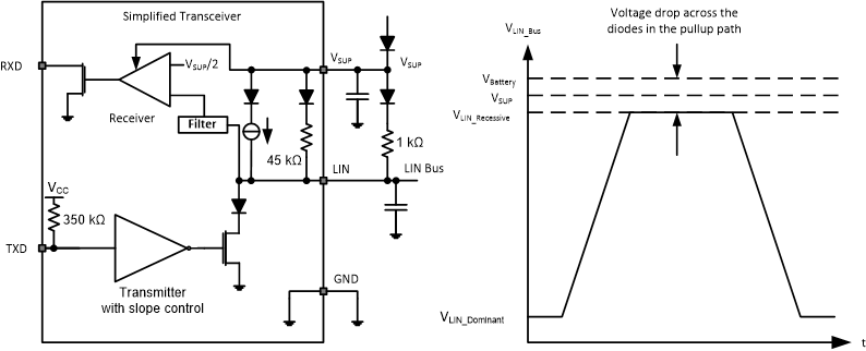
GUID-F3679A08-E3B8-40BB-81B9-89372E009501-low.gifFigure 9-3 Commander Node Configuration with Voltage Levels