ZHCSD39B November 2014 – August 2019 DS90UH929-Q1
PRODUCTION DATA.
- 1 特性
- 2 应用
- 3 说明
- 4 修订历史记录
- 5 Pin Configuration and Functions
-
6 Specifications
- 6.1 Absolute Maximum Ratings
- 6.2 ESD Ratings
- 6.3 Recommended Operating Conditions
- 6.4 Thermal Information
- 6.5 DC Electrical Characteristics
- 6.6 AC Electrical Characteristics
- 6.7 DC And AC Serial Control Bus Characteristics
- 6.8 Recommended Timing for the Serial Control Bus
- 6.9 Timing Diagrams
- 6.10 Typical Characteristics
-
7 Detailed Description
- 7.1 Overview
- 7.2 Functional Block Diagram
- 7.3
Feature Description
- 7.3.1 High-Definition Multimedia Interface (HDMI)
- 7.3.2 Transition Minimized Differential Signaling
- 7.3.3 Enhanced Display Data Channel
- 7.3.4 Extended Display Identification Data (EDID)
- 7.3.5 Consumer Electronics Control (CEC)
- 7.3.6 +5-V Power Signal
- 7.3.7 Hot Plug Detect (HPD)
- 7.3.8 High-Speed Forward Channel Data Transfer
- 7.3.9 Back Channel Data Transfer
- 7.3.10 Power Down (PDB)
- 7.3.11 Serial Link Fault Detect
- 7.3.12 Interrupt Pin (INTB)
- 7.3.13 Remote Interrupt Pin (REM_INTB)
- 7.3.14 General-Purpose I/O
- 7.3.15 Backward Compatibility
- 7.3.16 Audio Modes
- 7.3.17 HDCP
- 7.3.18 Built-In Self Test (BIST)
- 7.3.19 Internal Pattern Generation
- 7.3.20 Spread Spectrum Clock Tolerance
- 7.4 Device Functional Modes
- 7.5
Programming
- 7.5.1 Serial Control Bus
- 7.5.2 Multi-Master Arbitration Support
- 7.5.3 I2C Restrictions on Multi-Master Operation
- 7.5.4 Multi-Master Access to Device Registers for Newer FPD-Link III Devices
- 7.5.5 Multi-Master Access to Device Registers for Older FPD-Link III Devices
- 7.5.6 Restrictions on Control Channel Direction for Multi-Master Operation
- 7.6 Register Maps
- 8 Application and Implementation
- 9 Power Supply Recommendations
- 10Layout
- 11器件和文档支持
- 12机械、封装和可订购信息
8.2 Typical Applications
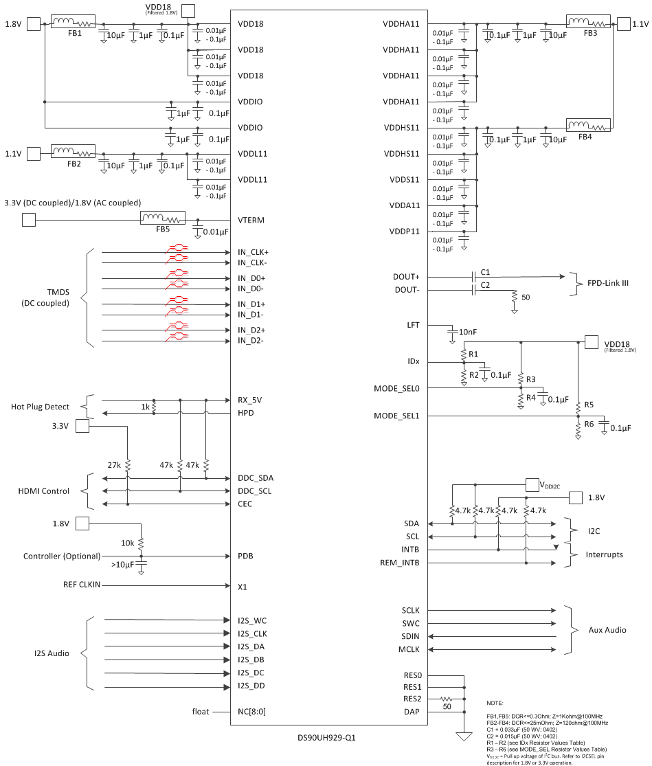
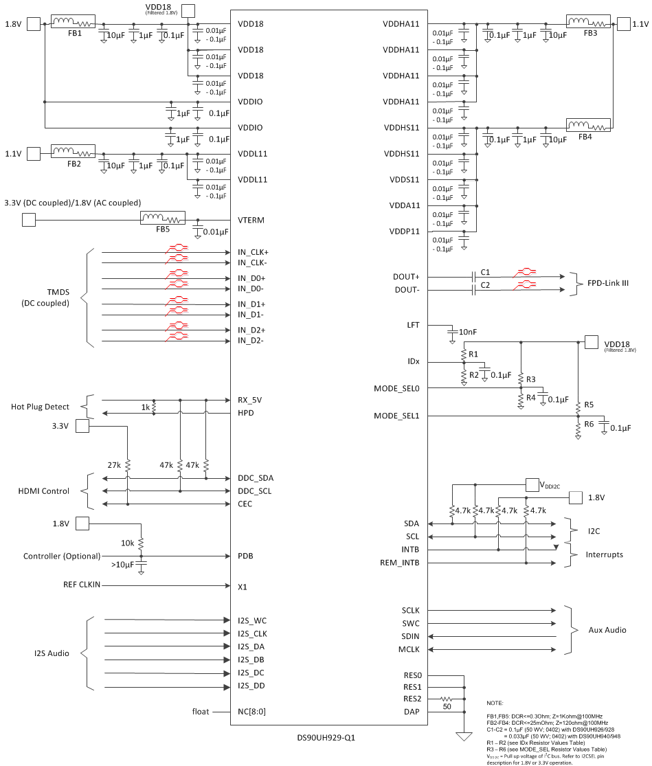
Bypass capacitors should be placed near the power supply pins. A capacitor and resistor are placed on the PDB pin to delay the enabling of the device until power is stable. See and for typical STP and coax connection diagrams.
 Figure 21. Typical Application Connection -- Coax
  Figure 22. Typical Application Connection -- STP
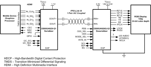
  Figure 23. Typical System Diagram