ZHCSCZ2A July 2014 – September 2014 DS125BR820
PRODUCTION DATA.
- 1 特性
- 2 应用
- 3 说明
- 4 修订历史记录
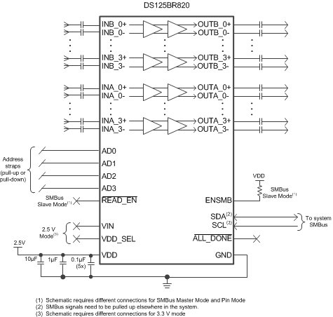
- 5 Pin Configuration and Functions
- 6 Specifications
- 7 Detailed Description
- 8 Applications and Implementation
- 9 Power Supply Recommendations
- 10Layout
- 11器件和文档支持
- 12机械封装和可订购信息
1 特性
2 应用
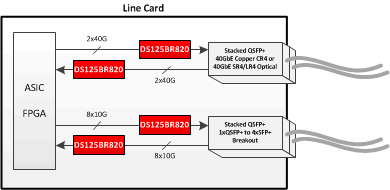
- 前端口 40G-CR4/SR4/LR4 链路扩展
- 背板 40G-KR4 链路扩展
- SAS/SATA/PCIe 链路扩展
- 其它速率高达 12.5Gbps 的专有高速接口
简化功能框图
3 说明
DS125BR820 是一款超低功耗高性能中继器/转接驱动器,专用于支持高速接口速率高达 12.5Gbps 的八个通道,例如 40G-CR4、40G-KR4、SAS/SATA 和 PCIe。 接收器的连续时间线性均衡器 (CTLE) 后接一个线性输出驱动器,可在 6GHz (12Gbps) 时提供 3dB 至 10dB 的可编程高频增强功能。 CTLE 接收器能够打开一个因码间干扰 (ISI)(由电路板迹线或铜质同轴电缆等互连介质引起)而完全关闭的输入眼型状态。 可编程的均衡能够可在互连通道内的实体布局方面实现最大限度的灵活性并提高通道的总体性能。
当在 40G-CR4/KR4、SAS/SATA 和 PCIe 应用中运行时,DS125BR820 保留发射信号特性,从而使得主机控制器和端点能够协商发射均衡器系数。 这个链路协商协议的透明管理有助于实现系统级互用性并最大限度缩短延迟。
可通过引脚控制、软件(SMBus 或 I2C)来轻松应用相关可编程设置,或者通过外部 EEPROM 直接加载设置。 在 EEPROM 模式下,配置信息在加电时自动加载,这样就免除了对于外部微控制器或软件驱动程序的需要。
器件信息(1)
| 器件型号 | 封装 | 封装尺寸(标称值) |
|---|---|---|
| DS125BR820 | WQFN (54) | 10mm x 5.5mm |
- 如需了解所有可用封装,请见数据表末尾的可订购产品附录。
典型应用方框图