• Menu
  • Product
  • Email
  • PDF
  • Order now
  • DRV8833C 双路 H 桥电机驱动器

    • ZHCSCV7 August   2014 DRV8833C

      PRODUCTION DATA.  

  • CONTENTS
  • SEARCH
  • DRV8833C 双路 H 桥电机驱动器
  1. 1 特性
  2. 2 应用
  3. 3 说明
  4. 4 修订历史记录
  5. 5 Pin Configuration and Functions
  6. 6 Specifications
    1. 6.1 Absolute Maximum Ratings
    2. 6.2 Handling Ratings
    3. 6.3 Recommended Operating Conditions
    4. 6.4 Thermal Information
    5. 6.5 Electrical Characteristics
    6. 6.6 Typical Characteristics
  7. 7 Detailed Description
    1. 7.1 Overview
    2. 7.2 Functional Block Diagram
    3. 7.3 Feature Description
      1. 7.3.1 PWM Motor Drivers
      2. 7.3.2 Bridge Control and Decay Modes
      3. 7.3.3 Current Control
      4. 7.3.4 Decay Mode
      5. 7.3.5 Slow Decay
      6. 7.3.6 Sleep Mode
      7. 7.3.7 Parallel Mode
      8. 7.3.8 Protection Circuits
        1. 7.3.8.1 Overcurrent Protection (OCP)
        2. 7.3.8.2 Thermal Shutdown (TSD)
        3. 7.3.8.3 UVLO
    4. 7.4 Device Functional Modes
  8. 8 Application and Implementation
    1. 8.1 Application Information
    2. 8.2 Typical Application
      1. 8.2.1 Design Requirements
      2. 8.2.2 Detailed Design Procedure
        1. 8.2.2.1 Stepper Motor Speed
        2. 8.2.2.2 Current Regulation
      3. 8.2.3 Application Curve
  9. 9 Power Supply Recommendations
    1. 9.1 Sizing Bulk Capacitance for Motor Drive Systems
  10. 10Layout
    1. 10.1 Layout Guidelines
    2. 10.2 Layout Example
  11. 11器件和文档支持
    1. 11.1 商标
    2. 11.2 静电放电警告
    3. 11.3 术语表
  12. 12机械封装和可订购信息
  13. 重要声明
search No matches found.
  • Full reading width
    • Full reading width
    • Comfortable reading width
    • Expanded reading width
  • Card for each section
  • Card with all content


DATA SHEET

DRV8833C 双路 H 桥电机驱动器

本资源的原文使用英文撰写。 为方便起见,TI 提供了译文;由于翻译过程中可能使用了自动化工具,TI 不保证译文的准确性。 为确认准确性,请务必访问 ti.com 参考最新的英文版本(控制文档)。

1 特性

  • 带电流控制的双 H 桥电机驱动器
    • 1 个或 2 个直流电机或者 1 个步进电机
    • 低导通电阻:高侧 + 低侧 (HS + LS) = 1735mΩ(25°C 时的典型值)
  • 输出电流能力(VM = 5V,25°C 时)
    • 散热薄型小外形尺寸 PWP (HTSSOP) 封装
      • 每个 H 桥的均方根 (RMS) 电流为 0.7A,峰值 1A
      • 并行模式下 RMS 为 1.4A
    • 四方扁平无引线 RTE (QFN) 封装
      • 每个 H 桥的均方根 (RMS) 电流为 0.6A,峰值 1A
      • 并行模式下 RMS 为 1.2A
  • 宽电源电压范围
    • 2.7V 至 10.8V
  • 集成电流调节
  • 简易脉宽调制 (PWM) 接口
  • 1.6µA 低电流睡眠模式(电压 5V 时)
  • 小型封装尺寸
    • 16HTSSOP (PowerPAD™) 5.00 × 6.40mm
    • 16 QFN (PowerPAD) 3.00 × 3.00mm
  • 保护特性
    • VM 欠压闭锁 (UVLO)
    • 过流保护 (OCP)
    • 热关断 (TSD)
    • 故障指示引脚 (nFAULT)

2 应用

  • 销售点打印机
  • 视频安保摄像机
  • 办公自动化设备
  • 游戏机
  • 机器人
  • 电池供电式玩具

3 说明

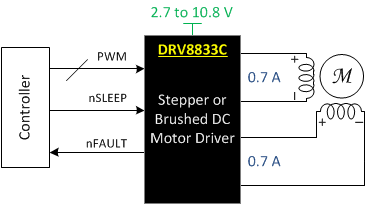
DRV8833C 为玩具、打印机及其他机电一体化应用提供了一款双桥电机驱动器解决方案。

该器件具有两个 H 桥驱动器,能够驱动两个直流电刷电机、一个双极性步进电机、螺线管或其它电感性负载。

每个 H 桥输出都包括一对 N 通道和 P 通道金属氧化物半导体场效应晶体管 (MOSFET) 以及用于调节绕组电流的电路。 借助正确的印刷电路板 (PCB) 设计,DRV8833C 的每个 H 桥能够持续驱动高达 700mA RMS(或 DC)(在 25°C 采用 5V VM 电源时)。该器件可支持每个 H 桥高达 1A 的峰值电流。 在较低的 VM 电压条件下,电流能力略有下降。

输出引脚发生故障时,还可提供用于过流保护、短路保护、UVLO 和过热保护的内部关断功能。 另外,还提供了一种低功耗睡眠模式。

器件信息(1)

部件号 封装 封装尺寸(标称值)
DRV8833C HTSSOP (16) 5.00mm x 6.40mm
四方扁平无引线 (QFN) (16) 3.00mm x 3.00mm
  1. 要了解所有可用封装,请见数据表末尾的可订购产品附录。
sch_FAD_LVSCP9.gif

4 修订历史记录

日期 修订版本 注释
2014 年 8 月 * 最初发布。

5 Pin Configuration and Functions

HTSSOP (PWP)
16 Pins
Top View
po_HTSSOP_LVSCP9.gif
QFN (RTE)
16 Pins
Top View
po_QFN_LVSCP9.gif

Pin Functions

PIN TYPE DESCRIPTION
NAME PWP RTE
POWER AND GROUND
GND 13 11 PWR Device ground Both the GND pin and device PowerPAD must be connected to ground
VINT 14 12 — Internal regulator (3.3 V) Internal supply voltage; bypass to GND with 2.2-μF, 6.3-V capacitor
VM 12 10 PWR Power supply Connect to motor supply voltage; bypass to GND with a 10-µF (minimum) capacitor rated for VM
CONTROL
AIN1 16 14 I H-bridge A PWM input Controls the state of AOUT1 and AOUT2; internal pulldown
AIN2 15 13
BIN1 9 7 I H-bridge B PWM input Controls the state of BOUT1 and BOUT2; internal pulldown
BIN2 10 8
nSLEEP 1 15 I Sleep mode input Logic high to enable device; logic low to enter low-power sleep mode; internal pulldown
STATUS
nFAULT 8 6 OD Fault indication pin Pulled logic low with fault condition; open-drain output requires an external pullup
OUTPUT
AISEN 3 1 O Bridge A sense Sense resistor to GND sets PWM current regulation level (seePWM Motor Drivers)
AOUT1 2 16 O Bridge A output Positive current is AOUT1 → AOUT2
AOUT2 4 2
BISEN 6 4 O Bridge B sense Sense resistor to GND sets PWM current regulation level (see PWM Motor Drivers)
BOUT1 7 5 O Bridge B output Positive current is BOUT1 → BOUT2
BOUT2 5 3

External Components

Component Pin 1 Pin 2 Recommended
CVM VM GND 10-µF(2) ceramic capacitor rated for VM
CVINT VINT GND 6.3-V, 2.2-µF ceramic capacitor
RnFAULT VINT(1) nFAULT >1 kΩ
RAISEN AISEN GND Sense resistor, see Typical Application for sizing
RBISEN BISEN GND Sense resistor, see Typical Application for sizing
(1) nFAULT may be pulled up to an external supply rated < 5.5 V.
(2) Proper bulk capacitance sizing depends on the motor power.

6 Specifications

6.1 Absolute Maximum Ratings

over operating free-air temperature (unless otherwise noted) (1)
MIN MAX UNIT
Voltage Power supply (VM) –0.3 11.8 V
Internal regulator (VINT) –0.3 3.8 V
Control pins (AIN1, AIN2, BIN1, BIN2, nSLEEP, nFAULT) –0.3 7 V
Continuous phase node pins (AOUT1, AOUT2, BOUT1, BOUT2) –0.3 VM + 0.5 V
Pulsed 10 µs phase node pins (AOUT1, AOUT2, BOUT1, BOUT2) –1 VM + 1 V
Continuous shunt amplifier input pins (AISEN, BISEN) –0.3 0.5 V
Pulsed 10 µs shunt amplifier input pins (AISEN, BISEN) –1 1 V
Peak drive current (AOUT1, AOUT2, BOUT1, BOUT2, AISEN, BISEN) Internally limited A
TJ Operating junction temperature –40 150 °C
(1) Stresses beyond those listed under Absolute Maximum Ratings may cause permanent damage to the device. These are stress ratings only, which do not imply functional operation of the device at these or any other conditions beyond those indicated under Recommended Operating Conditions. Exposure to absolute-maximum-rated conditions for extended periods may affect device reliability.

6.2 Handling Ratings

MIN MAX UNIT
Tstg Storage temperature range –65 150 °C
V(ESD) Electrostatic discharge Human body model (HBM), per ANSI/ESDA/JEDEC JS-001, all pins(1) –2000 2000 V
Charged device model (CDM), per JEDEC specification JESD22-C101, all pins(2) –1000 1000
(1) JEDEC document JEP155 states that 500-V HBM allows safe manufacturing with a standard ESD control process.
(2) JEDEC document JEP157 states that 250-V CDM allows safe manufacturing with a standard ESD control process.

6.3 Recommended Operating Conditions

over operating free-air temperature range (unless otherwise noted)
MIN MAX UNIT
VM Power supply voltage range(1) 2.7 10.8 V
VI Logic level input voltage 0 5.5 V
IRMS Motor RMS current(2) PWP package 0 0.7 A
RTE package 0 0.6 A
ƒPWM Applied PWM signal to AIN1, AIN2, BIN1, or BIN2 0 200 kHz
TA Operating ambient temperature –40 85 °C
(1) Note that when VM is below 5 V, RDS(ON) increases and maximum output current is reduced.
(2) Power dissipation and thermal limits must be observed.

6.4 Thermal Information

THERMAL METRIC(1) DRV8833C UNIT
HTSSOP QFN
16 PINS 16 PINS
RθJA Junction-to-ambient thermal resistance 40.5 44.7 °C/W
RθJC(top) Junction-to-case (top) thermal resistance 32.9 48.5
RθJB Junction-to-board thermal resistance 28.8 16.8
ψJT Junction-to-top characterization parameter 0.6 0.7
ψJB Junction-to-board characterization parameter 11.5 16.7
RθJC(bot) Junction-to-case (bottom) thermal resistance 4.8 4.2
(1) For more information about traditional and new thermal metrics, see the IC Package Thermal Metrics application report, SPRA953.

6.5 Electrical Characteristics

over operating free-air temperature range (unless otherwise noted)
PARAMETER TEST CONDITIONS MIN TYP MAX UNIT
POWER SUPPLIES (VM, VINT)
VM VM operating voltage 2.7 10.8 V
IVM VM operating supply current VM = 5 V, xINx low, nSLEEP high 1.7 3 mA
IVMQ VM sleep mode supply current VM = 5 V, nSLEEP low 1.6 2.7 μA
tSLEEP Sleep time nSLEEP low to sleep mode 10 µs
tWAKE Wake-up time nSLEEP high to output transition 155 μs
tON Turn-on time VM > VUVLO to output transition 25 μs
VINT Internal regulator voltage VM = 5 V 3 3.3 3.6 V
CONTROL INPUTS (AIN1, AIN2, BIN1, BIN2, nSLEEP)
VIL Input logic low voltage xINx 0 0.7 V
nSLEEP 0 0.5
VIH Input logic high voltage xINx 2 5.5 V
nSLEEP 2.5 5.5
VHYS Input logic hysteresis 350 400 650 mV
IIL Input logic low current VIN = 0 V –1 1 μA
IIH Input logic high current VIN = 5 V 50 μA
RPD Pulldown resistance xINx 100 150 250 kΩ
nSLEEP 380 500 750
tDEG Input deglitch time 575 ns
tPROP Propagation delay INx to OUTx VM = 5 V 1.2 μs
CONTROL OUTPUTS (nFAULT)
VOL Output logic low voltage IO = 5 mA 0.5 V
IOH Output logic high leakage RPULLUP = 1 kΩ to 5 V –1 1 μA
MOTOR DRIVER OUTPUTS (AOUT1, AOUT2, BOUT1, BOUT2)
RDS(ON) High-side FET on-resistance VM = 5 V, I = 0.2 A, TA = 25°C 1180 mΩ
VM = 5 V, I = 0.2 A, TA = 85°C(1) 1400 1475
VM = 2.7 V, I = 0.2 A, TA = 25°C 1550
VM = 2.7 V, I = 0.2 A, TA = 85°C(1) 1875 1975
RDS(ON) Low-side FET on-resistance VM = 5 V, I = 0.2 A, TA = 25°C 555 mΩ
VM = 5 V, I = 0.2 A, TA = 85°C(1) 675 705
VM = 2.7 V, I = 0.2 A, TA = 25°C 635
VM = 2.7 V, I = 0.2 A, TA = 85°C(1) 775 815
IOFF Off-state leakage current VM = 5 V –1 1 μA
tRISE Output rise time VM = 5 V; RL = 16 Ω to GND 70 ns
tFALL Output fall time VM = 5 V; RL = 16 Ω to VM 80 ns
tDEAD Output dead time Internal dead time 450 ns
PWM CURRENT CONTROL (AISEN, BISEN)
VTRIP xISEN trip voltage 160 200 240 mV
tOFF Current control constant off time Internal PWM constant off time 20 µs
PROTECTION CIRCUITS
VUVLO VM undervoltage lockout VM falling; UVLO report 2.6 V
VM rising; UVLO recovery 2.7
VUVLO,HYS VM undervoltage hysteresis Rising to falling threshold 90 mV
IOCP Overcurrent protection trip level 1 A
tDEG Overcurrent deglitch time 2.3 μs
tOCP Overcurrent protection period 1.4 ms
TTSD(1) Thermal shutdown temperature Die temperature, TJ 150 °C
THYS Thermal shutdown hysteresis Die temperature, TJ 20 °C
(1) Not tested in production; based on design and characterization data

6.6 Typical Characteristics

D001_SLVSCP9.gif
Figure 1. Supply Current
D004_SLVSCP9.gif
Figure 3. High-Side RDS(ON)
D003_SLVSCP9.gif
Figure 5. VINT Over VM
D002_SLVSCP9.gif
Figure 2. Sleep Current
D005_SLVSCP9.gif
Figure 4. Low-Side RDS(ON)

7 Detailed Description

7.1 Overview

The DRV8833C device is an integrated motor driver solution for brushed DC or bipolar stepper motors. The device integrates two PMOS + NMOS H-bridges and current regulation circuitry. The DRV8833C can be powered with a supply voltage from 2.7 to 10.8 V and can provide an output current up to 700 mA RMS.

A simple PWM interface allows easy interfacing to the controller circuit.

The current regulation is a 20-µs fixed off-time slow decay.

The device includes a low-power sleep mode, which lets the system save power when not driving the motor.

7.2 Functional Block Diagram

fbd_LVSCP9.gif

7.3 Feature Description

7.3.1 PWM Motor Drivers

The DRV8833C contains drivers for two full H-bridges. Figure 6 shows a block diagram of the circuitry.

fbd_PWM_motor_LVSCP9.gifFigure 6. H-Bridge and Current-Chopping Circuitry

7.3.2 Bridge Control and Decay Modes

The AIN1 and AIN2 input pins control the state of the AOUT1 and AOUT2 outputs; similarly, the BIN1 and BIN2 input pins control the state of the BOUT1 and BOUT2 outputs (see Table 1).

Table 1. H-Bridge Logic

xIN1 xIN2 xOUT1 xOUT2 FUNCTION
0 0 Z Z Coast / fast decay
0 1 L H Reverse
1 0 H L Forward
1 1 L L Brake / slow decay

The inputs can also be used for PWM control of the motor speed. When controlling a winding with PWM and the drive current is interrupted, the inductive nature of the motor requires that the current must continue to flow (called recirculation current). To handle this recirculation current, the H-bridge can operate in two different states, fast decay or slow decay. In fast-decay mode, the H-bridge is disabled and recirculation current flows through the body diodes. In slow-decay mode, the motor winding is shorted by enabling both low-side FETs.

To externally pulse-width modulate the bridge in fast-decay mode, the PWM signal is applied to one xIN pin while the other is held low; to use slow-decay mode, one xIN pin is held high. See Table 2 for more information.

Table 2. PWM Control of Motor Speed

xIN1 xIN2 FUNCTION
PWM 0 Forward PWM, fast decay
1 PWM Forward PWM, slow decay
0 PWM Reverse PWM, fast decay
PWM 1 Reverse PWM, slow decay

The internal current control is still enabled when applying external PWM to xIN. To disable the current control when applying external PWM, the xISEN pins should be connected directly to ground. Figure 7 show the current paths in different drive and decay modes.

fwd_rev_decay_LVSCP9.gifFigure 7. Drive and Decay Modes

7.3.3 Current Control

The current through the motor windings may be limited, or controlled, by a 20-µs constant off-time PWM current regulation, or current chopping. For DC motors, current control is used to limit the start-up and stall current of the motor. For stepper motors, current control is often used at all times.

When an H-bridge is enabled, current rises through the winding at a rate dependent on the DC voltage and inductance of the winding. If the current reaches the current chopping threshold, the bridge disables the current until the beginning of the next PWM cycle. Note that immediately after the output is enabled, the voltage on the xISEN pin is ignored for a fixed period of time before enabling the current sense circuitry. This blanking time is fixed at 3.75 μs.

The PWM chopping current is set by a comparator that compares the voltage across a current sense resistor connected to the xISEN pins with a reference voltage. The reference voltage, VTRIP, is is fixed at 200 mV nominally.

The chopping current is calculated as in Equation 1.

Equation 1. eq_I_chop_LVSCP9.gif

Example: If a 1-Ω sense resistor is used, the chopping current will be 200 mV / 1 Ω = 200 mA.

NOTE

If current control is not needed, the xISEN pins should be connected directly to ground.

7.3.4 Decay Mode

After the chopping current threshold is reached, the H-bridge switches to slow-decay mode. This state is held for toff (20 µs) until the next cycle to turn on the high-side MOSFETs.

7.3.5 Slow Decay

In slow-decay mode, the high-side MOSFETs are turned off and both of the low-side MOSFETs are turned on. The motor current decreases while flowing in the two low-side MOSFETs until reaching its fixed off time (typically 20 µs). After that, the high-side MOSFETs are enabled to increase the winding current again.

tim_t_off_LVSCP9.gifFigure 8. Current Chopping Operation

7.3.6 Sleep Mode

Driving nSLEEP low puts the device into a low-power sleep state. In this state, the H-bridges are disabled, all internal logic is reset, and all internal clocks are stopped. All inputs are ignored until nSLEEP returns inactive high. When returning from sleep mode, some time, tWAKE, needs to pass before the motor driver becomes fully operational. To make the board design simple, the nSLEEP can be pulled up to the supply (VM). TI recommends to use a pullup resistor when this is done. This resistor limits the current to the input in case VM is higher than 6.5 V. Internally, the nSLEEP pin has a 500-kΩ resistor to GND. It also has a clamping Zener diode that clamps the voltage at the pin at 6.5 V. Currents greater than 250 µA can cause damage to the input structure. Therefore, TI recommends a pullup resistor between 20 to 75 kΩ.

7.3.7 Parallel Mode

The two H-bridges in the DRV8833C can be connected in parallel for double the current of a single H-bridge. The internal dead time in the DRV8833C prevents any risk of cross-conduction (shoot-through) between the two bridges due to timing differences between the two bridges. Figure 9 shows the connections.

sch_parallel_LVSCP9.gifFigure 9. Parallel Mode Schematic

7.3.8 Protection Circuits

The DRV8833C is fully protected against overcurrent, overtemperature, and undervoltage events.

7.3.8.1 Overcurrent Protection (OCP)

An analog current limit (IOCP) circuit on each FET limits the current through the FET by limiting the gate drive. If this analog current limit persists for longer than the OCP deglitch time (tDEG), all FETs in the H-bridge are disabled and the nFAULT pin is driven low. The driver is re-enabled after the OCP retry period (tOCP) has passed. nFAULT becomes high again after the retry time. If the fault condition is still present, the cycle repeats. If the fault is no longer present, normal operation resumes and nFAULT remains deasserted. Note that only the H-bridge in which the OCP is detected will be disabled while the other bridge functions normally.

Overcurrent conditions are detected independently on both high-side and low-side devices; a short to ground, supply, or across the motor winding all result in an overcurrent shutdown. Note that overcurrent protection does not use the current sense circuitry used for PWM current control, so it functions even without presence of the xISEN resistors.

7.3.8.2 Thermal Shutdown (TSD)

If the die temperature exceeds safe limits, all FETs in the H-bridge are disabled and the nFAULT pin is driven low. After the die temperature has fallen below the specified hysteresis (THYS), operation automatically resumes. The nFAULT pin is released after operation has resumed.

7.3.8.3 UVLO

If at any time the voltage on the VM pin falls below the UVLO threshold voltage, VUVLO, all circuitry in the device is disabled, and all internal logic is reset. Operation resumes when VM rises above the UVLO threshold. The nFAULT pin is not driven low during an undervoltage condition.

Table 3. Device Protection

Fault Condition Error Report H-Bridge Internal Circuits Recovery
VM undervoltage (UVLO) VM < 2.6 V None Disabled Disabled VM > 2.7 V
Overcurrent (OCP) IOUT > IOCP FAULTn Disabled Operating OCP
Thermal Shutdown (TSD) TJ > TTSD FAULTn Disabled Operating TJ < TTSD – THYS

7.4 Device Functional Modes

The DRV8833C is active unless the nSLEEP pin is brought logic low. In sleep mode, the H-bridge FETs are disabled (Hi-Z). Note that tSLEEP must elapse after a falling edge on the nSLEEP pin before the device is in sleep mode. The DRV8833C is brought out of sleep mode automatically if nSLEEP is brought logic high. Note that tWAKE must elapse before the outputs change state after wake-up.

Table 4. Modes of Operation

Fault Condition H-Bridge Internal Circuits
Operating nSLEEP pin high Operating Operating
Sleep mode nSLEEP pin low Disabled Disabled
Fault encountered Any fault condition met Disabled See Table 3

8 Application and Implementation

8.1 Application Information

The DRV8833C is used in stepper or brushed DC motor control. The following design procedure can be used to configure the DRV8833C in a bipolar stepper motor application.

8.2 Typical Application

typ_app_LVSCP9.gif

8.2.1 Design Requirements

Table 5 gives design input parameters for system design.

Table 5. Design Parameters

Design Parameter Reference Example Value
Supply voltage VM 9 V
Motor winding resistance RL 12 Ω/phase
Motor winding inductance LL 10 mH/phase
Motor full step angle θstep 1.8 °/step
Target stepping level nm 2 (half-stepping)
Target motor speed v 120 rpm
Target chopping current ICHOP 200 mA
Sense resistor RISEN 1 Ω

8.2.2 Detailed Design Procedure

8.2.2.1 Stepper Motor Speed

The first step in configuring the DRV8833C requires the desired motor speed and stepping level. The DRV8833C can support full- and half-stepping modes using the PWM interface.

If the target motor speed is too high, the motor does not spin. Ensure that the motor can support the target speed.

For a desired motor speed (v), microstepping level (nm), and motor full step angle (θstep),

Equation 2. eq_f_step_LVSCP9.gif
tim_full-step_LVSCP9.gifFigure 10. Full-Step Mode
tim_half-step_LVSCP9.gifFigure 11. Half-Step Mode

8.2.2.2 Current Regulation

The chopping current (ICHOP) is the maximum current driven through either winding. This quantity depends on the sense resistor value (RXISEN).

Equation 3. eq_I_chop_LVSCP9.gif

ICHOP is set by a comparator which compares the voltage across RXISEN to a reference voltage. Note that ICHOP must follow Equation 4 to avoid saturating the motor.

Equation 4. eq_I_fs_LVSCP9.gif

where

  • VM is the motor supply voltage.
  • RL is the motor winding resistance.

8.2.3 Application Curve

app_curve_1_LVSCP9.gif
A. Channel 1 is the AIN1 input PWM signal, and channel 2 is the AIN2 input PWM signal. BIN1 and BIN2 follow the same pattern, but are shifted by 90° from AIN1 and AIN2 as shown in Figure 11. Channel 4 is the output current in the direction AOUT1 → AOUT2. In forward and reverse drive, the current rises until it hits the current chopping limit of 200 mA, and is regulated at that level with fixed-off time current chopping.
Figure 12. ½ Stepping Operation


Texas Instruments

© Copyright 1995-2025 Texas Instruments Incorporated. All rights reserved.
Submit documentation feedback | IMPORTANT NOTICE | Trademarks | Privacy policy | Cookie policy | Terms of use | Terms of sale