ZHCSCR3C October 2012 – August 2014 DS125BR111
PRODUCTION DATA.
- 1 特性
- 2 应用
- 3 说明
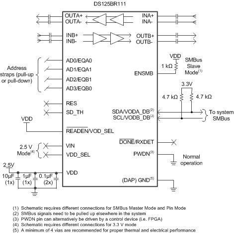
- 4 简化电路原理图
- 5 修订历史记录
- 6 Pin Configuration and Functions
- 7 Specifications
- 8 Detailed Description
- 9 Application and Implementation
- 10Power Supply Recommendations
- 11Layout
- 12器件和文档支持
- 13机械封装和可订购信息
1 特性
- 每通道 65mW(典型值)低功耗
- 支持链路协商
- 支持带外 (OOB) 信令
- 高级信号调节 I/O
- 6GHz 时,接收高达 10dB 的连续时间线性均衡器 (CTLE)
- 线性输出驱动器
- 输出电压范围超过 1200mV
- 可通过引脚选择、EEPROM 或 SMBus 接口进行编程
- 单电源电压:2.5V 或 3.3V
- -40°C 至 85°C 的工作温度范围
- 4mm x 4mm 24 引脚超薄型四方扁平无引线 (WQFN) 封装内的直通引脚分配
2 应用
- SAS-1/2/3 和 SATA-1/2/3
- PCI Express 1/2/3
- 其它速率高达 12.5Gbps 的专有接口
3 说明
DS125BR111 是一款超低功耗的高性能中继器/转接驱动器,旨在支持高达 12.5Gbps 的 1 通道高速接口。 6GHz 时,接收器的连续时间线性均衡器 (CTLE) 可在每个通道上提高 3-10dB。 在 SAS-3 或 PCIe Gen-3 应用中工作时,DS125BR111 保留发射信号特性,从而使得主机控制器和端点能够协商发射均衡器系数。 链接协商协议的透明度能够最大程度增加互连通道内器件实体布局的灵活性并提高通道的总体性能。
可通过引脚、软件(SMBus 或 I2C)来轻松应用相关可编程设置,或者通过外部 EEPROM 来载入此设置。 在 EEPROM 模式下,配置信息在加电时被自动载入,这样就免除了对于外部微控制器或软件驱动程序的需要。
器件信息(1)
| 器件型号 | 封装 | 封装尺寸(标称值) |
|---|---|---|
| DS125BR111 | WQFN (24) | 4.00mm x 4.00mm |
- 要了解所有可用封装,请见数据表末尾的可订购产品附录。
4 简化电路原理图