ZHCS322D May 2011 – December 2014 TPS62730 , TPS62732 , TPS62733
PRODUCTION DATA.
- 1 特性
- 2 应用
- 3 说明
- 4 修订历史记录
- 5 说明 (续)
- 6 Device Comparison Table
- 7 Pin Configuration and Functions
- 8 Specifications
- 9 Detailed Description
- 10Application and Implementation
- 11Power Supply Recommendations
- 12Layout
- 13器件和文档支持
- 14机械、封装和可订购信息
10 Application and Implementation
NOTE
Information in the following applications sections is not part of the TI component specification, and TI does not warrant its accuracy or completeness. TI’s customers are responsible for determining suitability of components for their purposes. Customers should validate and test their design implementation to confirm system functionality.
10.1 Application Information
The TPS62730 is a high-frequency synchronous step down DC-DC converter optimized for ultra low-power wireless applications. The device is optimized to supply TI's Low-Power Wireless sub 1-GHz and 2.4-GHz RF transceivers and system-on-chip (SoC) solutions.
10.2 Typical Application
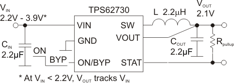 Figure 8. Typical Application
10.2.1 Design Requirements
The TPS6273x is a highly integrated DC-DC converter. The output voltage is internally fixed and does not require and external feedback divider network. For proper operation only a input- and output capacitor and an inductor is required. Table 1 shows the components used for the application characteristic curves.
Table 1. List of Components
| REFERENCE | DESCRIPTION | VALUE | MANUFACTURER | DIMENSIONS |
|---|---|---|---|---|
| TPS62730 | Step-down converter with bypass mode | Texas Instruments | 1.5 x 1.0 x 0.55 mm | |
| CIN, COUT | Ceramic capacitor 0402 X5R 6.3V GRM155R60J225 | 2.2 µF | Murata | 1.0 x 0.5 x 0.5 mm |
| L | Inductor MIPSZ2012 2R2 | 2.2 µH | FDK | 2.0 x 1.2 x 1.0 mm |
10.2.2 Detailed Design Procedure
10.2.2.1 Output Filter Design (Inductor and Output Capacitor)
The TPS62730 is optimized to operate with effective inductance values in the range of 1.5 μH to 3 μH and with effective output capacitance in the range of 1.0 μF to 10 μF. The internal compensation is optimized to operate with an output filter of L = 2.2 μH and COUT = 2.2 μF, which gives and LC output filter corner frequency of:

10.2.2.2 Inductor Selection
The inductor value affects its peak-to-peak ripple current, the PWM-to-PFM transition point, the output voltage ripple and the efficiency. The selected inductor must be rated for its DC resistance and saturation current. The inductor ripple current (ΔIL) decreases with higher inductance and increases with higher VI N or VO UT. Equation 4 calculates the maximum inductor current under static load conditions. The saturation current of the inductor should be rated higher than the maximum inductor current as calculated with Equation 5.

where
- f = Switching Frequency
- L = Inductor Value
- ΔIL= Peak-to-Peak inductor ripple current

where
- ΔIL= Peak-to-Peak inductor ripple current
- ILmax = Maximum Inductor current
In high-frequency converter applications, the efficiency is essentially affected by the inductor AC resistance (that is, quality factor) and to a smaller extent by the inductor DCR value. To achieve high efficiency operation, care should be taken in selecting inductors featuring a quality factor above 25 at the switching frequency. Increasing the inductor value produces lower RMS currents, but degrades transient response. For a given physical inductor size, increased inductance usually results in an inductor with lower saturation current.
The total losses of the coil consist of both the losses in the DC resistance, R(DC), and the following frequency-dependent components:
- The losses in the core material (magnetic hysteresis loss, especially at high switching frequencies)
- Additional losses in the conductor from the skin effect (current displacement at high frequencies)
- Magnetic field losses of the neighboring windings (proximity effect)
- Radiation losses
The following inductor series from different suppliers have been used with the TPS62730 converters.
Table 2. List of Inductors
| INDUCTANCE [μH] |
DIMENSIONS [mm3] |
INDUCTOR TYPE | SUPPLIER |
|---|---|---|---|
| 2.2 | 2.0 × 1.2 × 1.0 | LQM21PN2R2NGC | Murata |
| 2.2 | 2.0 × 1.2 × 1.0 | MIPSZ2012 | FDK |
10.2.2.3 DC-DC Output Capacitor Selection
The DCS-Control scheme of the TPS62730 allows the use of tiny ceramic capacitors. Ceramic capacitors with low ESR values have the lowest output voltage ripple and are recommended. The output capacitor requires either an X7R or X5R dielectric. Y5V and Z5U dielectric capacitors, aside from their wide variation in capacitance over temperature, become resistive at high frequencies. At light load currents the converter operate in power save mode and the output voltage ripple is dependent on the output capacitor value and the PFM peak inductor current.
10.2.2.4 Additional Decoupling Capacitors
In addition to the output capacitor there are further decoupling capacitors connected to the output of the TPS62730. These decoupling capacitor are placed closely at the RF transmitter or micro controller. The total capacitance of these decoupling capacitors should be kept to a minimum and should not exceed the values given in the reference designs, see Figure 31 and Figure 32. During mode transition from DC-DC operation to bypass mode the capacitors on the output VOUT are charged up to the battery voltage VIN through the internal bypass switch. During mode transition from bypass mode to DC-DC operation, these capacitors must be discharged by the system supply current to the nominal output voltage threshold until the DC-DC converter will kick in. The charge change in the output and decoupling capacitors can be calculated according to Equation 6. The energy loss due to charge and discharge of the output and decoupling capacitors can be calculated according to Equation 7.

where
- dQCOUT_CDEC : Charge change needed to charge up and discharge the output and decoupling capacitors from VOUT_DC_DC to VIN and vice versa
- CCOUT_CDEC: Total capacitance on the VOUT pin of the device, includes output and decoupling capacitors
- VIN: Input (battery) voltage
- VOUT_DC_DC: nominal DC-DC output voltage VOUT

where
- CCOUT_CDEC: Total capacitance on the VOUT pin of the device, includes output and decoupling capacitors
- VIN: Input (battery) voltage
- VOUT_DC_DC: nominal DC-DC output voltage VOUT
10.2.2.5 Input Capacitor Selection
Because of the nature of the buck converter having a pulsating input current, a low ESR input capacitor is required for best input voltage filtering to ensure proper function of the device and to minimize input voltage spikes. For most applications a 2.2 µF to 4.7 µF ceramic capacitor is recommended. The input capacitor can be increased without any limit for better input voltage filtering.
Table 3 shows a list of tested input/output capacitors.
10.2.2.5.1 Input Buffer Capacitor Selection
In addition to the small ceramic input capacitor a larger buffer capacitor CBuf is recommended to reduce voltage drops and ripple voltage. When using battery chemistries like Li-SOCl2, Li-SO2, Li-MnO2, the impedance of the battery must be considered. These battery types tend to increase their impedance depending on discharge status and often can support output currents of only a few mA. Therefore a buffer capacitor is recommended to stabilize the battery voltage during DC-DC operations (for example, for an RF transmission). A voltage drop on the input of the TPS62730 during DC-DC operation impacts the advantage of the step-down conversion for system power reduction. Furthermore the voltage drops can fall below the minimum recommended operating voltage of the device and leads to an early system cut off. Both impacts effects reduce the battery life time. To achieve best performance and to extract most energy out of the battery, a good procedure is to design the select the buffer capacitor value for an voltage drop below 50 mVpp during DC-DC operation. The capacitor value strongly depends on the used battery type, as well the current consumption during an RF transmission as well the duration of the transmission.
Table 3. List of Capacitor
| CAPACITANCE [μF] | SIZE | CAPACITOR TYPE | SUPPLIER |
|---|---|---|---|
| 2.2 | 0402 | GRM155R60J225 | Murata |
10.2.2.6 Checking Loop Stability
The first step of circuit and stability evaluation is to look from a steady-state perspective at the following signals:
- Switching node, SW
- Inductor current, IL
- Output ripple voltage, VOUT(AC)
Basic signals must be measured when evaluating a switching converter. When the switching waveform shows large duty cycle jitter or the output voltage or inductor current shows oscillations, the regulation loop may be unstable. This is often a result of board layout and/or L-C combination.
As a next step in the evaluation of the regulation loop, the load transient response is tested. The time between the application of the load transient and the turn on of the High Side MOSFET, the output capacitor must supply all of the current required by the load. VOUT immediately shifts by an amount equal to ΔI(LOAD) x ESR, where ESR is the effective series resistance of COUT. ΔI(LOAD) begins to charge or discharge CO generating a feedback error signal used by the regulator to return VOUT to its steady-state value. The results are most easily interpreted when the device operates in PWM mode.
During this recovery time, VOUT can be monitored for settling time, overshoot or ringing that helps judge the converter’s stability. Without any ringing, the loop has usually more than 45° of phase margin.
Because the damping factor of the circuitry is directly related to several resistive parameters (for example, MOSFET rDS(on)) that are temperature dependant, the loop stability analysis must be done over the input voltage range, load current range, and temperature range.
10.2.3 Application Curves
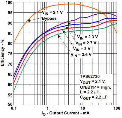 Figure 9. Efficiency vs Output Current
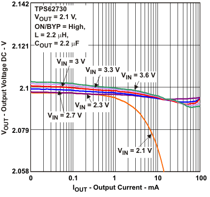 Figure 11. Output Voltage vs Output Current
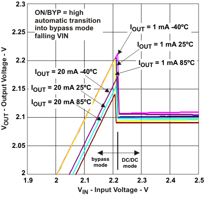 Figure 13. Automatic Transition into Bypass Mode - Falling VIN
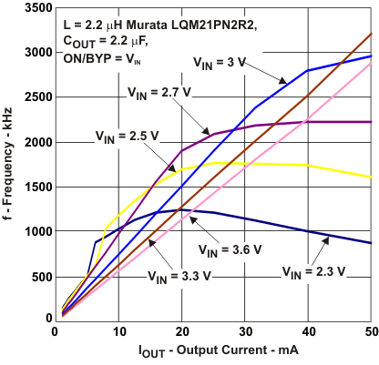 Figure 15. Switching Frequency vs IOUT vs VIN
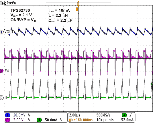 Figure 19. DC-DC Mode Operation IOUT = 10 mA
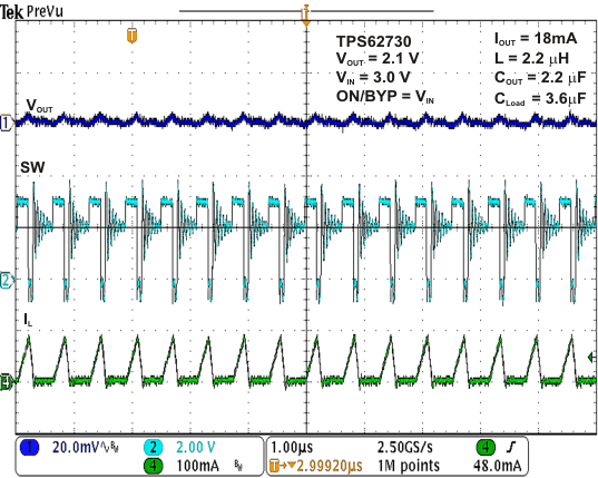 Figure 21. DC-DC Mode Operation IOUT = 18 mA
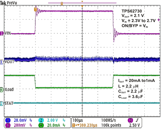 Figure 23. DC-DC Mode Operation Line and Load Transient Performance
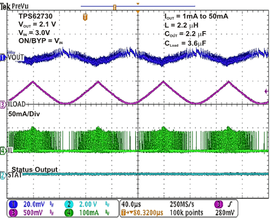 Figure 25. DC-DC Mode VOUT AC Load Regulation Performance
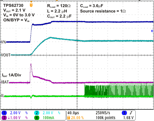 Figure 27. Start-Up Behavior
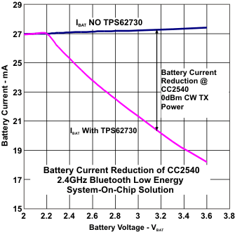 Figure 29. Battery Current Reduction vs Battery Voltage
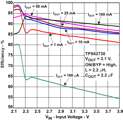 Figure 10. Efficiency vs Input Voltage
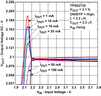 Figure 12. Output Voltage vs Input Voltage
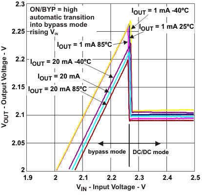 Figure 14. Automatic Transition into Bypass Mode - Rising VIN
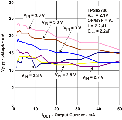 Figure 16. VOUT vs IOUT vs VIN
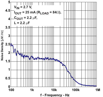 Figure 18. Noise Density vs Frequency
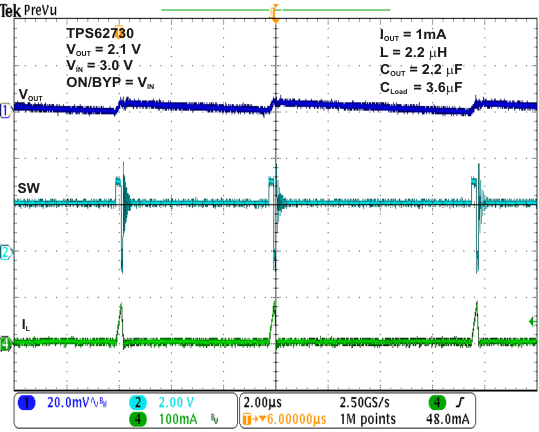 Figure 20. DC-DC Mode Operation IOUT = 1 mA
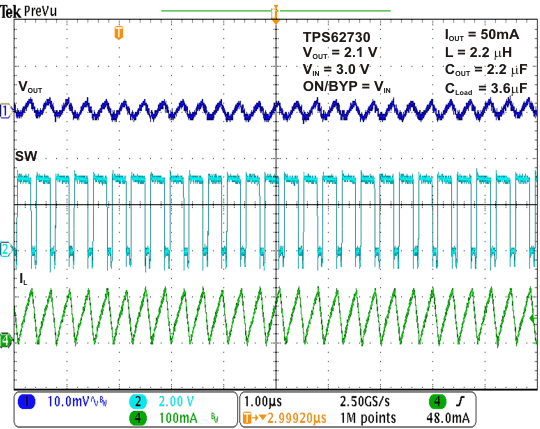 Figure 22. DC-DC Mode Operation IOUT = 50 mA
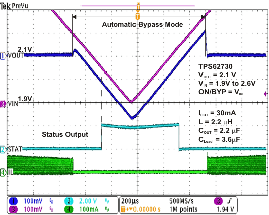 Figure 24. Automatic Bypass Transition with Falling / Rising Input Voltage VIN
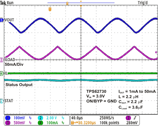 Figure 26. Bypass Mode Operation VOUT AC Behavior ON/BYP = GND
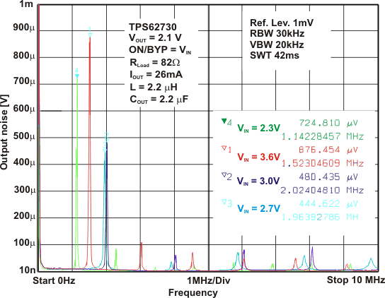 Figure 28. Spurious Output Noise TPS62730 IOUT 26 mA
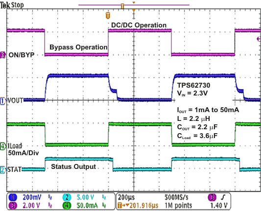 Figure 30. Mode Transition ON/BYP Behavior
10.3 System Examples
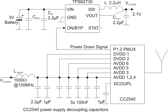 Figure 31. System Example CC2540
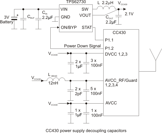 Figure 32. System Example CC430