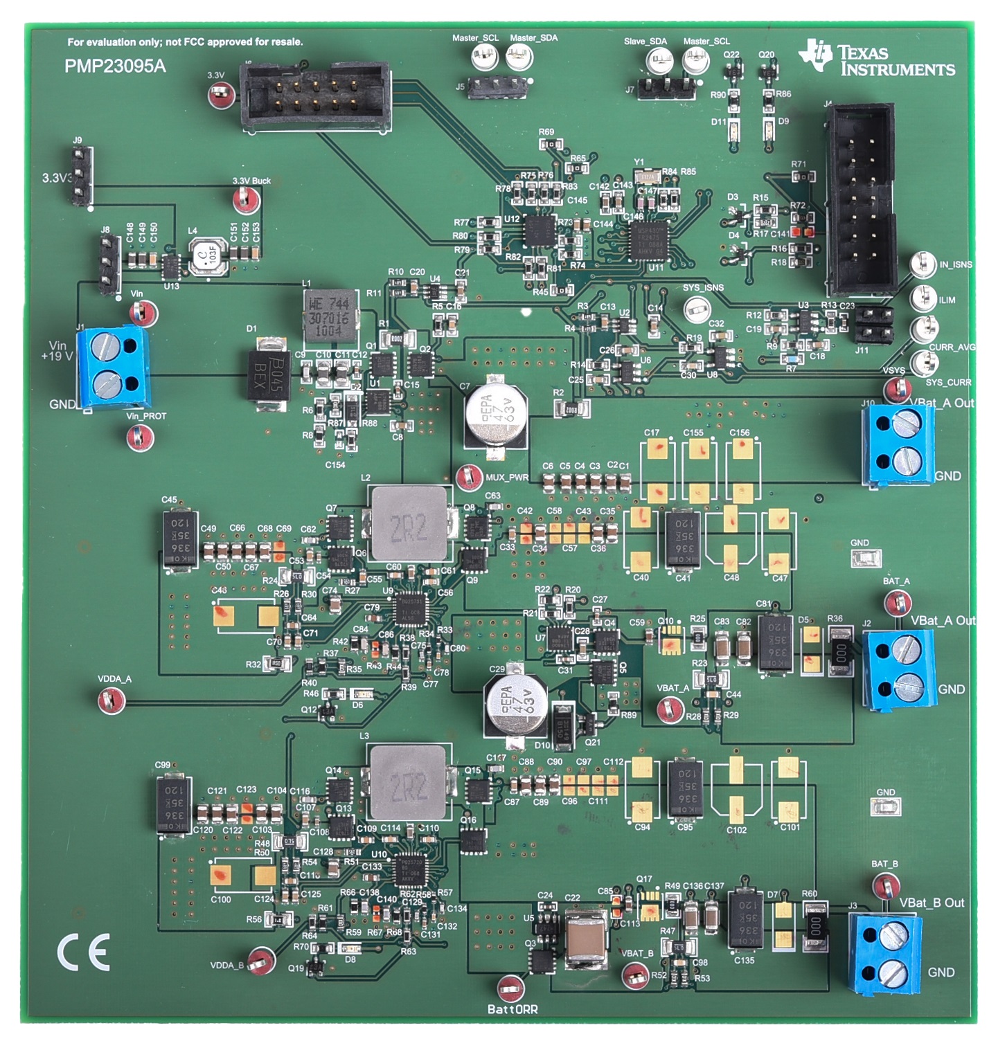
This reference design is a smart high-efficiency charger design for dual smart battery packs of up to 100 Watt hours (Wh) implemented as 1S–5S Lithium-ion (Li-ion) batteries in a parallel configuration. To achieve this an onboard MCU manages the communication and safety features needed for the charging system to interface with a battery pack designed to the Smart Battery Data Specification Revision 1.1 (SBD 1.1). This communication allows the MCU to initialize two independent battery charger ICs to the correct charging parameters, as well as inhibit charging when the batteries are outside of safe specifications. This design also demonstrates a high-efficiency system power MUX for selecting between the input adapter and efficient discharge of the two smart batteries simultaneously. These features make this reference design highly applicable for portable medical devices, such as oxygen concentrators.
TIDA-010240 | Design Folder |
BQ25731 | Product Folder |
LM7480-Q1, LM74700-Q1 | Product Folder |
MSP430FR2475, PCA9546A | Product Folder |
All portable equipment carried in aircrafts – including life-critical medical equipment such as portable ventilators, electrocardiogram devices (ECGs), and continuous positive-airway-pressure (CPAP) machines – are subjected to safety restrictions implemented by the Transportation Security Administration (TSA). Lithium batteries with more than 100 watt-hours (Wh) are generally not permitted in carry-on luggage, and any exceptions to this rule lie at the discretion of airlines and require prior approval. This disruption is not ideal for passengers who require these devices out of medical necessity. With the capabilities of Li-ion battery charging technology today, medical instrument manufacturers can alleviate this patient burden. To satisfy travel restrictions while also doubling the backup time of the equipment, two 100-Wh batteries can be implemented in the system design. This configuration will also require fewer spare batteries, increasing convenience for the end user during travel. This design guide details the implementation of two BQ25731 chargers managed by an onboard MCU to achieve these requirements for airline travel.
Figure 2-2 illustrates the input and battery MUX circuit schematic.
The reference design board includes a screw terminal (J1) for input connections to a power supply. This board was tested with supplies ranging from 12 V to 19 V, but can function with inputs of 11 V to 22 V. The design also includes a barrel jack connector (J12) for easy connection to existing adapters. There is also a common PI filter at the input of this board for EMI filtering.
Calculate the corner frequency for a PI filter using Equation 1.
In this case, L1 = 160 nH and C10, C11 = 22 μF, resulting in a corner frequency of about 85 kHz.
For reverse polarity protection (RVP) the LM74800 (U1) monitors the voltage across Q1. When the reverse voltage across Q1, monitored with the A and C pins, exceeds –4.5 mV, the device turns off Q1 using the DGATE pin. This circuit acts a high-efficiency replacement for a Schottky diode.
After the reverse polarity protection, a 2-mΩ sense resistor is added to monitor the overall system input current. After this sense resistor, a VIN_PROT rail is defined. The VIN_PROT rail acts as an always on supply from the input with reverse polarity protection. This rail directly powers the BQ25731 charger devices.
To discharge the two independent batteries in the design, an ideal diode-ORing circuit is used. In this circuit, Q3 and Q4 are driven by U5 and U7 to regulate the FET forward voltage drop to 20 mV. This allows for the efficient discharge of both batteries at the same time, while also preventing current from traveling from one battery to the other. This circuit also allows for passive battery pack voltage balancing to occur in the system by drawing more current from the battery with a higher voltage. Equation 2 shows an example calculation of battery discharge current based on voltage and equivalent series resistance (ESR). For this example, it is assumed that BAT_A is at 16.8 V and has an ESR of 50 mΩ, BAT_B is at 16.6 V and also has an ESR of 50 mΩ, and the system is drawing 8 A.
In this example, BAT_A supplies 2 A more current that BAT_B until the higher current discharge causes the voltage differential between the batteries to be reduced.
This design provides an input and battery MUX that prioritizes the input adapter in all cases where the adapter voltage exceeds the UVLO setting of U1. When the UVLO threshold is triggered, the input adapter is disconnected from the system and the batteries are connected to power the system load. This prevents the batteries from discharging while an input adapter is present.
This threshold is set by the resistor divider consisting of R87 and R88. For U1 (input adapter connection) the UVLO thresholds are 1.13 V falling for turn off, and 1.23 V rising for turn on. For U7 (battery connection) the OV pin is connected to the same divider and the thresholds operate inversely. These thresholds are 1.13 V falling for turn on, and 1.23 V rising for turn off. In the schematic this voltage is connected to the net labeled UV/OV_SET. In the current schematic the switchover from input adapter to battery is triggered when VIN reaches 10.56 V and the switchover from battery to input adapter is triggered when VIN reaches 11.5 V.
Equation 3 shows an example of the resistor divider calculation:
The HGATE design for U1 includes two back-to-back NFETs (Q2 and Q11). Q11 was added to the design to prevent any current from flowing from the batteries to the VIN_FLT rail when the batteries are connected to the system. When only Q2 is placed and (V_SYS > VIN_PROT + 0.8 V) a current is conducted through the body diode of Q2. This allows a current loop to form between the output of both BQ25731 devices and the input of the BQ25731 devices.
Adjustments were made to the HGATE design of U7 to reduce the turn on time of Q5. This reduction is made by increasing the gate current delivered to Q5 from 55 μA to 600 μA. To increase the HGATE current that can be delivered by U7, a circuit including D10, Q21, and R84 was added. This circuit amplifies the source current of the HGATE pin by driving an NPN transistor (Q21) that is connected between the charge pump output (CAP, U7 pin 11) and the gate of Q5. A series resistance (R84) is also added to this path to limit the current injection. Diode (D10) is also added between the gate of Q5 and HGATE (U7 pin 8) to allow the HGATE pin to sink current when turning the FET off. Equation 4 provides an example calculation for the HGATE current injection limit. The charge pump of the LM74800 provides an output of VS + 13.2 V. In this case VS is connected to the output of the batteries and is assumed to be 16.8 V. The charge pump can supply a maximum current of 2.4 mA. The current design has the injection current set to be 600 μA, but this current can be increased by reducing R84.
Example 1.
Example 2.
Figure 2-3 illustrates the BQ25731 component selection.
Components for the BQ25731 Charge Controllers were selected to be as flexible as possible for this reference design. For a more detailed guide on component selection specific to your design, see the Detailed Design Procedure section in the BQ25731 I2C 1- to 5-Cell Buck-Boost Battery Charge Controller with USB-C PD 3.0 OTG Output data sheet.
For this design a circuit was added to limit the system current to 8 A. This is most impactful when the device is being used with a 12-V car adapter and can pull the battery voltage below the input threshold of the system. This circuit includes the INA213B to amplify the current across a 2-mΩ sense resistor. This INA213B has a gain of 50 V/V so an input of 8 A results in an 800-mV output.
To convert this signal into a usable voltage for the ILIM pin of the BQ25731 devices, an op amp configured as a difference amplifier was used. The voltage on the BQ25731 ILIM pin is converted to charge current based on Equation 5.
where
For the difference amplifier when:
where
To correctly set the BQ25731 charge current, set the ILIM pin at 1.0 V with 8 A of system current and 1.8 V with 0-A system current. Limit the charge current for each of the 2 charger devices to between 0 A and 4 A.
Set V2 at 1.8 V in this case. With V2 at 1.8 V, the voltage at the amplifiers positive input is equal to V2/2, which is 0.9 V. This voltage then needs to be created with the system 3.3-V rail and a resistor divider to match the calculated set point. This was implemented with a R7 and R9 as shown in the schematic above.