SPRUJ22A November 2021 – March 2023 AWR2944
- Trademarks
- 1Getting Started
-
2Hardware
- 2.1 Block Diagram
- 2.2 PCB Handling Recommendations
- 2.3 Power Connections
- 2.4
Connectors
- 2.4.1 MIPI 60-Pin Connector (J19)
- 2.4.2 Debug Connector-60 pin (J7)
- 2.4.3 CAN-A Interface Connector (J3)
- 2.4.4 CAN-B Interface Connector (J2)
- 2.4.5 Ethernet Ports (J4 and J9)
- 2.4.6 USB Connectors (J8, J10)
- 2.4.7 OSC_CLKOUT Connector (J14)
- 2.4.8 PMIC SPI Connector (J16) (DNP)
- 2.4.9 Voltage Rails Ripple Measurement Connectors (J1, J5) (DNP)
- 2.5 Antenna
- 2.6 PMIC
- 2.7 On-Board Sensors
- 2.8 PC Connection
- 2.9 Connecting the AWR2944EVM to the DCA1000 EVM
- 2.10 Jumpers, Switches, and LEDs
- 3Design Files and Software Tools
- 4Revision History
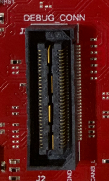
2.4.2 Debug Connector-60 pin (J7)
This connector enables interfacing of LVDS signals to the DCA1000 EVM for data capturing purposes.
Also, the connector has SPI, I2C, JTAG, GPADC, WRMRST, NRROUT, EPWM, and other control signals from AWR2944EVM for debug purpose.
The SPI is multiplexed to the Debug Connector. For more details refer to Section 2.8.1.
 Figure 2-6 60-pin Debug Connector
Table 2-2 provides the pin assignment details for the Debug 60-pin connector.
Table 2-2 J7 Pin Assignment
| Pin Number | Description | Pin Number | Description |
|---|---|---|---|
| 1 | NC | 2 | NC |
| 3 | NC | 4 | XREF_CLK0 |
| 5 | GND | 6 | MSS_EPWMA0 |
| 7 | DBG_SPI_CS0 | 8 | GND |
| 9 | DBG_SPI_CLK | 10 | MSS_SPIA_HOSTIRQ |
| 11 | DBG_SPI_PICO | 12 | DBG_SPI_POCI |
| 13 | 3.3V PULL_UP | 14 | XREF_CLK1 |
| 15 | EMU_TCK | 16 | MCU_CLKOUT |
| 17 | EMU_TDI | 18 | GND |
| 19 | GPADC1 | 20 | EMU_TMS |
| 21 | GPADC2 | 22 | EMU_TDO |
| 23 | GPADC3 | 24 | GND |
| 25 | GPADC4 | 26 | LVDS_TX3_FRCLK_P |
| 27 | GPADC5 | 28 | LVDS_TX3_FRCLK_N |
| 29 | GPADC6 | 30 | GND |
| 31 | GPADC7 | 32 | NC |
| 33 | GPADC8 | 34 | NC |
| 35 | GPADC9 | 36 | GND |
| 37 | MSS_SPIB_CS1 | 38 | NC |
| 39 | SOP1_MSS_SPIB_CS2 | 40 | NC |
| 41 | MSS_GPIO_0 | 42 | GND |
| 43 | MSS_GPIO_1 | 44 | LVDS_TX2_CLK_P |
| 45 | AR_WRMRST | 46 | LVDS_TX2_CLK_N |
| 47 | NC | 48 | GND |
| 49 | AR_NERROUT | 50 | LVDS_TX1_P |
| 51 | MSS_I2CA_SCL | 52 | LVDS_TX1_N |
| 53 | MSS_I2CA_SDA | 54 | |
| 55 | MSS_EPWMB0 | 56 | LVDS_TX0_P |
| 57 | MSS_EPWMA1 | 58 | LVDS_TX0_N |
| 59 | MSS_GPIO_3 | 60 | GND |