SNAU260A October 2020 – February 2021 LMK5C33216
ADVANCE INFORMATION
- Trademarks
- 1Introduction
- 2EVM Quick Start
- 3EVM Configuration
-
4EVM Schematics
- 4.1 Power Supply Schematic
- 4.2 Power Distribution Schematic
- 4.3 LMK5C33216 and Input Reference Inputs IN0 to IN1 Schematic
- 4.4 Clock Outputs OUT0 to OUT3 Schematic
- 4.5 Clock Outputs OUT4 to OUT9 Schematic
- 4.6 Clock Outputs OUT10 to OUT15 Schematic
- 4.7 XO Schematic
- 4.8 Logic I/O Interfaces Schematic
- 4.9 USB2ANY Schematic
- 5EVM Bill of Materials
- 6Appendix A - TICS Pro LMK5C33216 Software
- 7Revision History
3.1 Power Supply
The LMK5C33216 has VDD and VDDO supply pins that operate from 3.3 V ± 5%.
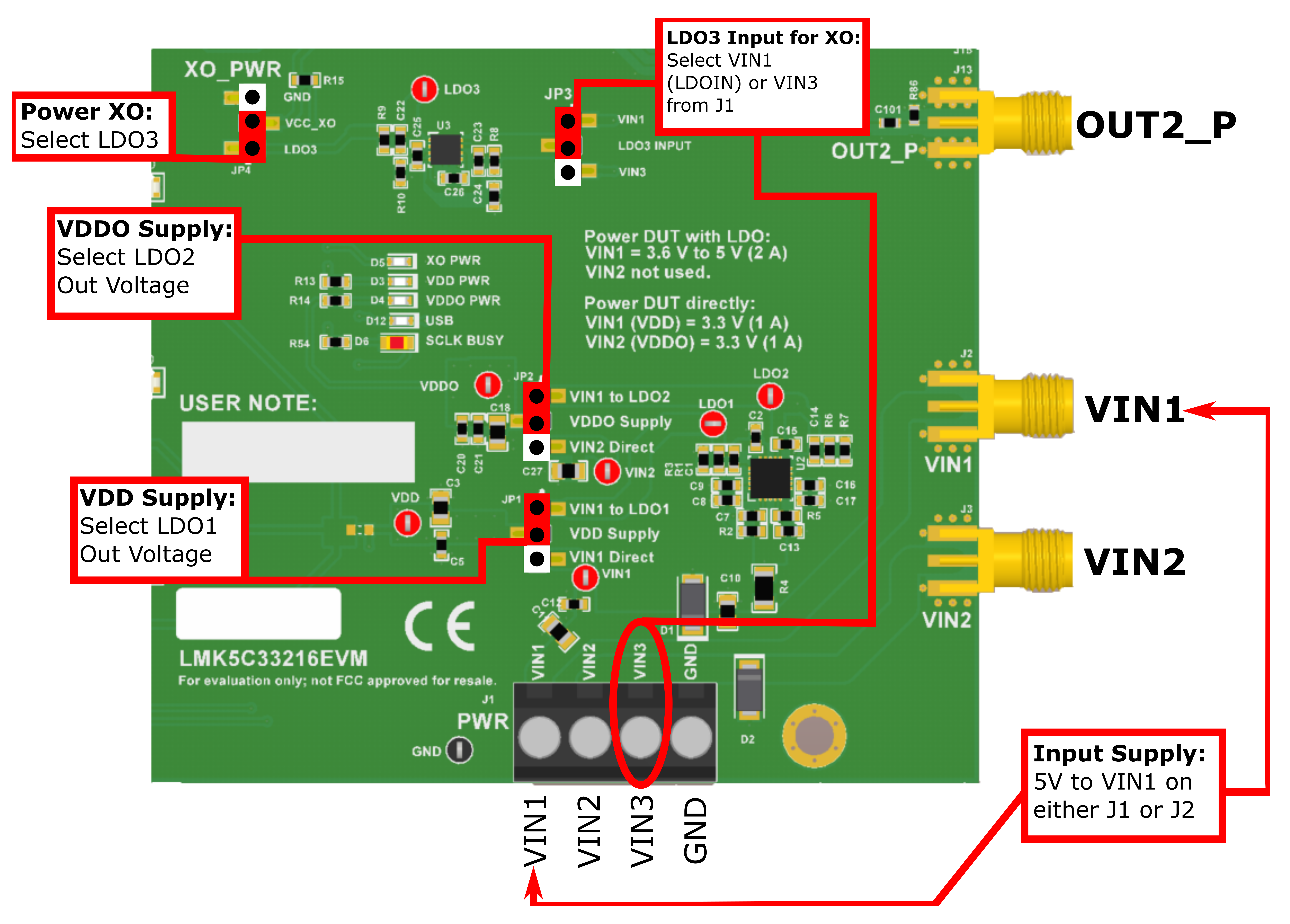
J1 is the main power terminal to the external power supply. Power SMA port VIN1 (J2) provides an alternative connector style to apply power through coax cable. By default this SMA connector is not populated.
On the EVM, the default power configuration uses the onboard LDO regulators to power all VDD and VDDO pins from an external 5-V supply input VIN1 to J1 (or J2). A Dual LDO regulator (U3) is used to power the VDD and VDDO rails of the DUT and its peripheral circuitry. A separate LDO regulator (U4),also supplied from VIN1, is used to power the onboard XO circuits.
 Figure 3-2 Default Power Jumper
Configuration
Figure 3-2 Default Power Jumper
ConfigurationFigure 3-2 shows the default power jumper locations and settings. Table 3-2 shows the suggested power configurations for the DUT.
| CONNECTION | NAME | ONBOARD LDO REGULATORS (DEFAULT) |
DIRECT EXTERNAL SUPPLIES |
|---|---|---|---|
| VD = 3.3 V (LDO1) VDDO = 3.3 V (LDO2) |
VDD = 3.3 V (EXT. VIN1) VDDO = 3.3 V (EXT. VIN2) |
||
| J1 | PWR | Pin 1 (VIN1): Connect to
external 5-V supply Pin 2 (VIN2): n/a Pin 3 (VIN3): n/a Pin 4 (GND): Connect to supply ground |
Pin 1 (VIN1): Connect to
external 3.3-V supply Pin 2 (VIN2): Connect to external 3.3-V supply Pin 3 (VIN3): n/a Pin 4 (GND): Connect to supply ground |
| JP1 | VDD | Tie pins 1-2 (adjacent to designator) to select 3.3 V from LDO1 to VDD Plane | Tie pins 2-3 (opposite to designator) to select external VIN1 to VDD Plane |
| JP2 | VDDO | Tie pins 1-2 (adjacent to designator) to select 3.3 V from LDO2 to VDDO Plane | Tie pins 2-3 (opposite to designator) to select external VIN2 to VDDO Plane |