SLUAAF1 May 2021 TPS62933
5 Thermal Performance
TPS54335A, TPS56339 and TPS62933 can all be applied in 19V/5V case. TPS54335A uses wire bonding SO Power PAD 8 package, its synchronous MOSFETs’ RDSons are 128mΩ and 84mΩ which are not that small and will do harm to the thermal performance. The thermal PAD can help a lot with the cooling. But TPS54335A is vulnerable to its big size which is 4.89mm×3.9mm.
TPS56339 uses FCOL SOT236 package whose size is 1.6mm×2.9mm which is much smaller than SOP 8 package. Although it does not have a thermal PAD due to the limited size and flip chip package, it’s RDSon of the high side FET and low side FET is 70mΩ and 35mΩ respectively which is much smaller than that of TPS54335A.
TPS62933, as is mentioned before, whose size is the smallest. Its synchronous MOSFETs’ RDSon is 80mΩ and 32mΩ respectively. The RDSon of the low side FET is smaller than that of TPS56339, which will do good to the thermal performance since the low side MOSFET turns on much longer than the high side MOSFET in low duty cycle cases.
To figure out the thermal performance of the three parts mentioned above, thermal scans are shown in Figure 5-1, Figure 5-2 and Figure 5-3 respectively in the test condition listed in Table 5-1.
| TPS62933 | TPS56339 | TPS54335A | |
|---|---|---|---|
| FCOL SOT583 | FCOL SOT263 | Bonding wire SOP8 | |
| Vin | 19V | 19V | 19V |
| Vout | 5V | 5V | 5V |
| Iout | 3A | 3A | 3A |
| Frequency | 500kHz | 500kHz | 500kHz |
| Inductor | 6.8µH | 6.8µH | 6.8µH |
| Size of PCB | 65mm×65mm | 65mm×65mm | 63mm×63mm |
| Total numbers of layers | 2 | 2 | 2 |
| Width of copper | 2oz | 2oz | 2oz |
 Figure 5-1 Thermal Scan of TPS62933
EVM
Figure 5-1 Thermal Scan of TPS62933
EVM Figure 5-2 Thermal Scan of TPS56339
EVM
Figure 5-2 Thermal Scan of TPS56339
EVM Figure 5-3 Thermal scan of TPS54335A
EVM.
Figure 5-3 Thermal scan of TPS54335A
EVM.All ICs were mounted on the similar size evaluation board whose information is listed in table2. The layout was optimized for good thermal performance based on guidelines mentioned in Section 4. The bonding wire SOP8 shows the highest temperature and FCOL SOT23 shares a similar performance. The FCOL SOT583 package hotspot is 3°C cooler than the bonding wire SOP8 and FCOL SOT236. This is benefit from the low RDSon of the low side MOSFET.
RθJA is the thermal resistance of the junction to the environment in still air conditions and is the most common thermal parameter for the semiconductor package. In most cases, the total heat of the device is eventually distributed into the air, so the air temperature is easy to measure or pre-determined and the junction temperature can be easily estimated with RθJA as long as the power consumption is known. The equation usually assumed to be valid for calculating junction temperature from RθJA is Equation 1 .
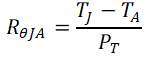
Where, PT is the total chip dissipated power, TJ is the temperature of the junction and TA is the ambient temperature.
Table 5-2 gives the thermal resistance based on EVM layout. From the test result the TPS62933 has the lowest thermal performance at full loading conditions.
| TPS62933 | TPS56339 | TPS54335A | |
|---|---|---|---|
| FCOL SOT583 | FCOL SOT263 | Bonding wire SOP8 | |
| TA | 27.7°C | 27.7°C | 27.7°C |
| TJ | 79.1°C | 88°C | 93.4°C |
| PJ | 0.816W | 0.85W | 1.66W |
| RθJA | 62.99°C/W | 70.89°C/W | 39.51°C/W |