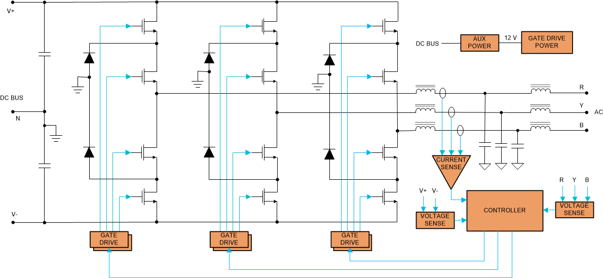
Figure 5-4 illustrates the basic topology of the Neutral Point Clamped inverter. This is also a multilevel topology like the TNPC inverter except that all switches of this topology are rated to half the bus voltage. The voltage stress on the devices is the lowest among all the topologies discussed so far.
Since only half of the voltage has to be switched, the switching losses in the transistor get reduced by half. In the NPC topology shown, it is possible to use 600-V components instead of 1200-V types. The 600-V technology has much faster components than are available in 1200-V technology. This will lead to further reduction in switching losses. This topology has lower ripple in the output current and only half of the output voltage transient. This will reduce the effort for filtering and isolation in the filter inductor. Hence we can achieve high power density with less inductance needed to maintain harmonic distortion in output. Multilevel inverters not only generate the output voltages with very low distortion, but also can minimize the dv/dt stresses across devices thereby reducing electromagnetic interference (EMI). This topology also offers bidirectional transfer of power and is the preferred choice for switching frequencies higher than 50 kHz due to lower switching losses and better efficiency. One drawback of the NPC topology is the high number of power semiconductor switches needed. Even though lower voltage rated devices can be used in a multilevel converter, each of the switches needs a gate drive circuit. This topology makes up for the complexity in its implementation by improved power density, higher efficiency as well as overall reduced system cost that comes from design of smaller size magnetics/passive components and fewer cooling needs. As this topology uses both controlled switches and diodes, the loss distribution is unsymmetrical and hence thermal management can be quite challenging. This topology being a bidirectional DC/AC topology is an option to consider for the bidirectional DC/AC stage (see
Figure 3-1) between the HV DC Bus and the AC Bus in a storage ready solar inverters.
 Figure 5-4 Neutral Point Clamped Inverter.