SLAU780 August   2018


  1.   MSP432E411Y-BGAEVM User's Guide
    1.     Trademarks
    2. 1 Board Overview
    3. 2 Power the MSP432E411Y-BGAEVM
      1. 2.1 Emulator Power
      2. 2.2 External 3.3-V Source Only
      3. 2.3 External 5-V Source Only
      4. 2.4 External 3.3-V and 5-V Source
      5. 2.5 Measure Current Consumption
    4. 3 Header Pinouts and Connections
      1. 3.1 J11 – External Power Connector
      2. 3.2 J6 – Power Rail Header
      3. 3.3 J7 – External Peripheral Interface Header
      4. 3.4 LCD Interface Header
      5. 3.5 J1, J2, J3, J4 – BoosterPack Interface Headers
      6. 3.6 J5 – Additional GPIO Pin Header
    5. 4 Communication Interfaces
      1. 4.1 Ethernet
      2. 4.2 USB-OTG
    6. 5 Programming Interfaces
      1. 5.1 JTAG
      2. 5.2 ETM Trace
      3. 5.3 BSL
    7. 6 Software Development
      1. 6.1 Software Description
      2. 6.2 Source Code
      3. 6.3 Tool Options
    8. 7 Schematics

J6 – Power Rail Header

Header J6 contains connections for all the power rails and reference voltages used by the MSP432E411Y device. Figure 4 shows header J6 and Table 3 lists the pinout.
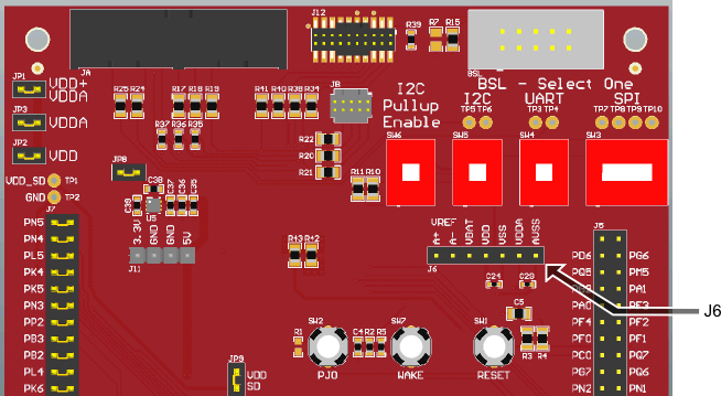
external-power-connector-j6.pngFigure 4. External Power Connector J6

Table 3. External Power Connector J6 Pinout

J6 Pin Signal Description
1 VREFA+ Reference voltage for ADC positive input
2 VREFA- Reference voltage for ADC negative input
3 VBAT Power source for hibernation module
4 VDD Positive supply for I/O
5 VSS Negative supply for I/O
6 VDDA Positive supply for analog circuits
7 AVSS Negative supply for analog circuits