SCES531L December 2003 – May 2017 SN74AVC2T45
PRODUCTION DATA.
- 1 Features
- 2 Applications
- 3 Description
- 4 Revision History
- 5 Pin Configuration and Functions
-
6 Specifications
- 6.1 Absolute Maximum Ratings
- 6.2 ESD Ratings
- 6.3 Recommended Operating Conditions
- 6.4 Thermal Information
- 6.5 Electrical Characteristics
- 6.6 Switching Characteristics: VCCA = 1.2 V
- 6.7 Switching Characteristics: VCCA = 1.5 V ±0.1 V
- 6.8 Switching Characteristics: VCCA = 1.8 V ±0.15 V
- 6.9 Switching Characteristics: VCCA = 2.5 V ±0.2 V
- 6.10 Switching Characteristics: VCCA = 3.3 V ±0.3 V
- 6.11 Operating Characteristics
- 6.12
Typical Characteristics
- 6.12.1 Typical Propagation Delay (A to B) vs Load Capacitance, TA = 25°C, VCCA = 1.2 V
- 6.12.2 Typical Propagation Delay (A to B) vs Load Capacitance, TA = 25°C, VCCA = 1.5 V
- 6.12.3 Typical Propagation Delay (A-to-B) vs Load Capacitance, TA = 25°C, VCCA = 1.8 V
- 6.12.4 Typical Propagation Delay (A to B) vs Load Capacitance, TA = 25°C, VCCA = 2.5 V
- 6.12.5 Typical Propagation Delay (A to B) vs Load Capacitance, TA = 25°C, VCCA = 3.3 V
- 7 Parameter Measurement Information
- 8 Detailed Description
- 9 Application and Implementation
- 10Power Supply Recommendations
- 11Layout
- 12Device and Documentation Support
- 13Mechanical, Packaging, and Orderable Information
11 Layout
11.1 Layout Guidelines
To ensure reliability of the device, following common printed-circuit board layout guidelines is recommended.
- Bypass capacitors should be used on power supplies. Place the capacitors as close as possible to the VCCA, VCCB pin and GND pin.
- Short trace lengths should be used to avoid excessive loading.
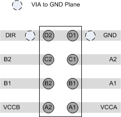
11.2 Layout Example
 Figure 16. Layout Example for YZP Package