SBOA422 March 2021 ADS8588S , ADS8688A , INA148 , INA826 , OPA197
Supporting High-Voltage Common Mode Using Difference Amplifier
Supporting high-voltage common-mode input in programmable logic controller (PLC) analog input modules improves reliability in noisy industrial environments.
The most cost effective way to support high-common mode is through a difference amplifier as shown in the circuit found in Figure 1-1.
 Figure 1-1 Differential Amplifier
A rail-to-rail input amplifier like OPA197 or OPA187 can be used along with matched resistors to form this difference amplifier. The gain of this circuit is represented as:

Common-Mode (CM) Range
The common-mode range limits are determined by the amplifier inputs limits. It’s easy to show that V1, and V2 have different limits for maximum input range, with V2 being more limited. Simple calculation with VREF = 0 leads to:
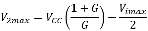
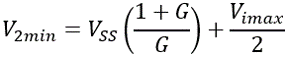
with G=1, Vimax=10, and ±15-V supply are assumed, V2 range is ±25 V.
Input Impedance
Input impedance of the circuit in Figure 1-1 is:
Achieving high-input impedance dictates the use of a high value input resistor as will as feedback resistor. The high-value feedback resistor decreases the bandwidth of the circuit as will be discussed later.
Ri=Rf=1MΩ 0.1% standard resistors have been chosen to maintain high-impedance input.
Offset Error
While input impedance is determined only by the front end, both front end and the ADC are affecting other parameters like offset and gain errors. Figure 1-2 shows the front end connected to the multiplexed input ADS8688 sampling at 500 kSPs.
 Figure 1-2 Front end Connected to
ADS8688
Figure 1-2 Front end Connected to
ADS8688Using the sum of squares, we can calculate the overall offset of the signal chain as:

Where ADC offset is input-referred, and amplifier offset is output-referred which equals amplifier offset multiplied by the noise gain. Both ADC and amplifier offsets and offset drifts are found in respective data sheets.
Typical ADC offset for ±10 V input range is ±0.5 mV and drift is only ±1ppm/°C, OPA197 has a typical offset of ±25 µV, and drift of ±0.5 µV /°C.
Multiplying the amplifier input offset drift by the noise gain result in ±1 µV/°C, which represents 0.1 ppm /°C relative to the ±10 V input range.
The typical values means both initial offset and offset drift will be dominated by ADC offset, The ADC offset drift over a temperature range of -40°C to 85°C is ±125 ppm = +0.63 mV.
It’s worth noting that worst-case offset values are way above this. However, the worst-case values are too pessimistic and typical values are much more realistic.
CM-related Offset Error
When CM voltage is added to a zero input voltage, another component of offset is introduced due to the input resistors mismatch which is dependent on the common-mode gain.

Where ΔR/R is the resistor tolerance, and α is a factor equals 4 in case of worst-case calculation, and 0.33 for the typical case. CM-induced offset error can be calculated by multiplying this gain by the common-mode range.

Using 0.1% resistors, and a CMR=±25 V, VOS|CM= ±8.25 mV. The op amps offset itself will increase in case of wide common-mode, but the resistor mismatch dominates the offset error. This type of offset error cannot be eliminated by calibration.
Gain Error
For the full chain, gain error consists of two components: resistors, and the ADC

The resistors gain error εG can be evaluated using Monte-Carlo simulation from the resistor tolerance (0.1%) Simulation shows a distribution with a three-sigma value of 0.125%. The ADC typical gain error is 0.02%FS. To some extent ADC gain error is negligible. The resistors tolerance translates to 12.5 mV gain error in case of 10-V input range.
In case of non-zero common-mode, the CM-related offset error would appear as gain error, by adding both values, the full-scale error would be close to 18 mV or 0.18%.
Signal Bandwidth
The signal goes over two subsequent filters through the signal chain. 1. The bandwidth of the difference amplifier, 2. The bandwidth of the ADS8688.
- The bandwidth (BW) of the difference amplifier is dominated by the Resistor-Capacitor (RC) filter composed of the feedback resistor (1MΩ) and the intrinsic output capacitance of the OPA197. Unfortunately, the output capacitance is not specified.
- ADS8688 has an integrated filter with 15-kHz bandwidth.
We will rely on measurement to determine the bandwidth; it has to be below 15 kHz.
Common-Mode Rejection Ratio
It can be proven that CMRR due to resistor mismatch (Rf and Rf', Ri and Ri') equals

Typical value calculation leads to CMRRR=3784 (71.5 dB)
Test Results
The analog signal chain shown in Figure 1-2 is put under test to validate calculations presented in this article. Note that some statistical parameters like offset error cannot be really validated using a single device sample.
| Parameter | Measured Value | Unit |
|---|---|---|
| VOS | -0.03 to -0.5 | mV |
| VOS|CM(±20V) | 2.5 to 3.1 | mV |
| εG | -0.1 to +0.02 | %FSR |
| εFS | -0.16 to +0.03 | %FSR |
| BW | 9.7 | kHz |
| tsettle | 130 | μs |
| CMRR | 77 | dB |
| Crosstalk | -82 | dB |
| 3rd HD | -106 | dB |
Table 1-1 shows the measured parameters of a few input channels attached to one ADC. Measured results to a great extent match our previous calculation. This architecture is a simple implementation for wide common-mode support, however there is a tradeoff between its bandwidth and its input impedance.
As the offset voltage mainly determined by the ADC in the circuit presented here, lower cost generic amplifiers with more relaxed offset specification can be explored without negatively affecting the performance. This circuit can also be used with a low-voltage ADC with a gain lower than one. This has the positive effect of improving the bandwidth.The techniques introduced in this document can also be applied to the difference amplifiers listed in TI Difference Amplifiers.
| Related devices | Description |
|---|---|
| OPA187 | 0.001-µV/°C Drift, Low Power, Rail-to-Rail Output 36-V Operational Amplifiers Zero-Drift Series |
| OPA196 | 36-V, Low-Power, Low Offset Voltage (100 μV), Rail-to-Rail Operational Amplifier |
| OPA991 | 40-V Rail-to-Rail Input/Output, Low Offset Voltage (125 μV), Low Noise (10.8 nV/√Hz) Op Amp |
References