SBAU412 November 2022 AFE7900 , AFE7903 , AFE7906 , AFE7920 , AFE7950
- Abstract
- Trademarks
- 1 Introduction
- 2 Prerequisites
- 3 Typical Bare-Metal Design Flow
- 4 Background
- 5 AFE SPI IP Container Pinout
- 6 TI AFE SPI IP Container
- 7 Create Block Designs With TI AFE SPI IP
- 8 Create New Platforms in Vitis
- 9 Create New Application Projects in Vitis
- 10Build Application Projects
- 11Configure the AXI GPIO
- 12Configure the AXI SPI
- 13Create Boot Images to Run on SD Card
- 14Set up and Power on Hardware
- 15Set up ZCU102 Board Interface for VADJ_FMC
- 16Debug Application Projects and Set up Vitis Serial Terminal
- 17Execute the Application
7 Create Block Designs With TI AFE SPI IP
The IP is expected to be used only within a block design. Users can create a new block design or instantiate the IP within an existing one. To create a new block design with the IP, follow these steps:
- Open the IP INTEGRATOR menu and click Create Block Design (see Figure 7-1).
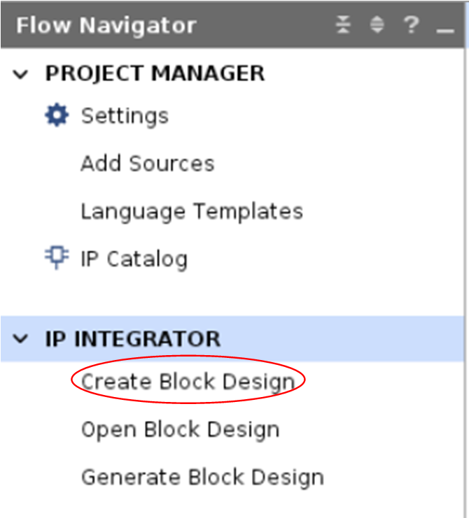 Figure 7-1 Creating Block Design
 - Enter the desired design name (see Figure 7-2) and keep the other two options as defaults. Click OK.
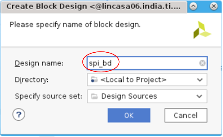 Figure 7-2 Naming of Block Design
 - Click the IP Catalog tab and notice the User Repository header (see Figure 7-3). The header appears only if the inclusion of the IP repository is done correctly, as explained in previous steps.
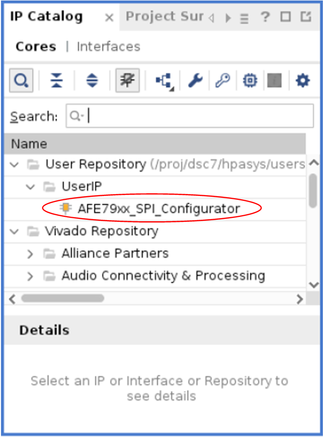 Figure 7-3 User Repository
 - Double-click AFE79xx SPI Configurator to launch the Add IP window.
- Click Add IP to Block Design (see Figure 7-4).
 Figure 7-4 Adding IP to Block Design
 - The AFE SPI IP shows up in the block design (see Figure 7-5) if the previous steps were followed correctly.
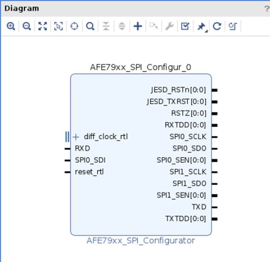 Figure 7-5 Final Diagram
The required IOs from the IP must be brought to the top-level file in the FPGA hdl design hierarchy. To do this, first make the required IOs as external. To make the required IOs as external, right-click the individual IOs of interest and select Make External (see Figure 7-6).
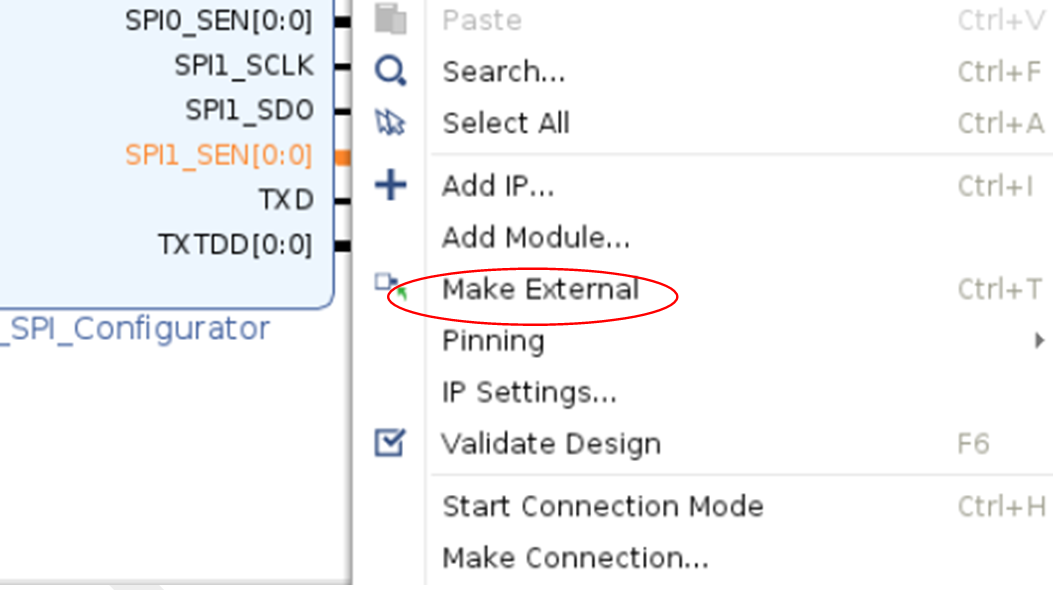 Figure 7-6 Making IOs External
In the above implementation example, the bare minimum required IOs are brought out as external.
The block design must then be validated for any errors and output products to generate. To validate the block diagram, right-click the block design under the Design Sources header.
Similarly, right-click the View Instantiation Template to use as a reference for wiring this block design on the top level hdl (see Figure 7-7).
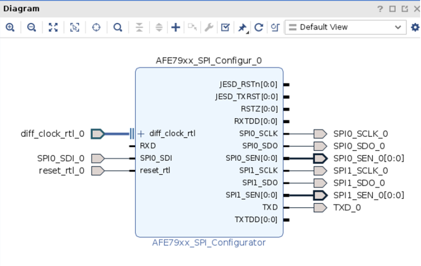 Figure 7-7 TI SPI Configurator Pinout
The IOs from the top level hdl which are connected to this IP must be declared in a Constraints file for them to be mapped to the hardware design, specific FPGA pins, and the correct IO levels.
The above steps complete the hardware design using TI AFE SPI IP.