SBAU412 November 2022 AFE7900 , AFE7903 , AFE7906 , AFE7920 , AFE7950
- Abstract
- Trademarks
- 1 Introduction
- 2 Prerequisites
- 3 Typical Bare-Metal Design Flow
- 4 Background
- 5 AFE SPI IP Container Pinout
- 6 TI AFE SPI IP Container
- 7 Create Block Designs With TI AFE SPI IP
- 8 Create New Platforms in Vitis
- 9 Create New Application Projects in Vitis
- 10Build Application Projects
- 11Configure the AXI GPIO
- 12Configure the AXI SPI
- 13Create Boot Images to Run on SD Card
- 14Set up and Power on Hardware
- 15Set up ZCU102 Board Interface for VADJ_FMC
- 16Debug Application Projects and Set up Vitis Serial Terminal
- 17Execute the Application
5 AFE SPI IP Container Pinout
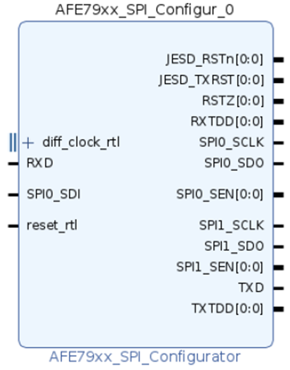
Table 5-1 Pinout Signals and Connections
| SIGNALS | DIRECTION | EXTERNAL CONNECTIONS |
|---|---|---|
| SPI0_SCLK, SPI0_SDO*, SPI0_SEN | Output | AFE SPI lines (_SDO* to SDI of AFE) |
| SPI0_SDI | Input | AFE SDO |
| SPI1_SCLK, SPI1_SDO, SPI1_SEN | Output | LMK SPI lines |
| RSTZ | Output | RESETn of AFE |
JESD RSTn JESD TXRST | Output | JESED IP Cores RSTn and TX Rst |
| RXD | Input | UART Terminal TX for debug |
| TXD | Output | UART Terminal RX for debug |
| diff_clock_rtl | Input | 100-Mhz differential clocking |
| Reset_rtl | Input | Reset (Active High) typically connected to FPGA board reset |