SBAA541 December 2022 AMC1202 , AMC1302 , AMC1306M05 , AMC22C11 , AMC22C12 , AMC23C10 , AMC23C11 , AMC23C12 , AMC23C14 , AMC23C15 , AMC3302 , AMC3306M05
- Abstract
- Trademarks
- 1Introduction
-
2Current Sensing in AC/DC Converters
- 2.1 Basic Hardware and Control Description of AC/DC
- 2.2 Point A and B – AC/DC AC Phase-Current Sensing
- 2.3 Point C and D – AC/DC DC Link Current Sensing
- 2.4 Summary of Positives and Negatives at Point A, B, C1/2 and D1/2 and Product Suggestions
- 3Current Sensing in DC/DC Converters
- 4Conclusion
- 5References
3.1 Basic Operation Principle of Isolated DC/DC Converter With Phase-Shift Control
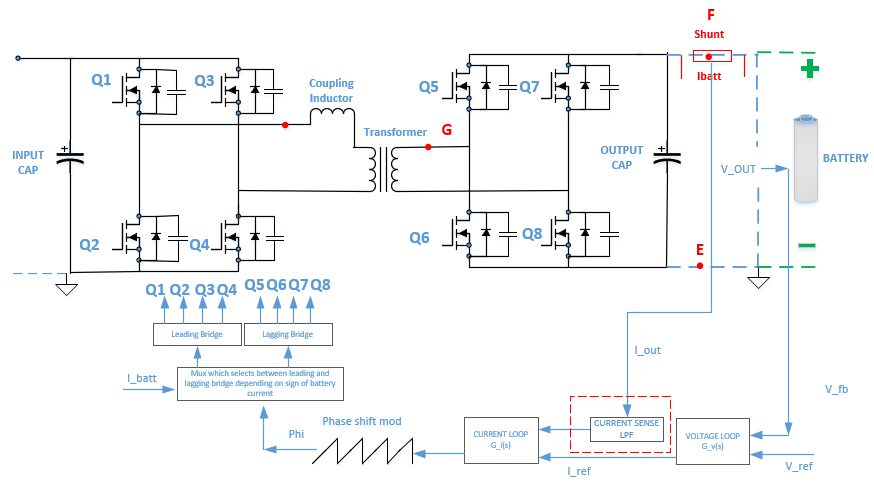
Figure 3-1 shows a typical control loop of a phase-shift dual active bridge (DAB) DC/ DC converter. There are two control loops in this system: (a) an outer voltage loop and (b) an inner current loop.
For the voltage loop, the output voltage is fed into an ADC of a MCU (denoted as Vfb) in Figure 3-1. Vfb is compared with a reference voltage (denoted as Vref). The error between the measured voltage and reference voltage is fed to a compensator, which can be realized as a PID controller. The output of the voltage loop is used as reference (Iref) for the inner current loop. The compensator of the inner current loop (GI) compares the reference (Iref) and actual value of sensed current (IOUT) and uses this error to adjust the phase of a PWM waveform to the leading or lagging bridge depending on the direction of the current. For constant current charging, the voltage loop is optional or can be implemented for protections only. For constant power charging, both loops are needed. The theoretical limits for the phase shift are ±π, practical implementations are much smaller than this.
 Figure 3-1 Typical Control Loop of Dual Active Bridge
(DAB) DC/DC Converter With Phase-Shift Control